EP1256990A2 - High contrast light-emitting diode devices - Google Patents
High contrast light-emitting diode devices Download PDFInfo
- Publication number
- EP1256990A2 EP1256990A2 EP02076723A EP02076723A EP1256990A2 EP 1256990 A2 EP1256990 A2 EP 1256990A2 EP 02076723 A EP02076723 A EP 02076723A EP 02076723 A EP02076723 A EP 02076723A EP 1256990 A2 EP1256990 A2 EP 1256990A2
- Authority
- EP
- European Patent Office
- Prior art keywords
- layer
- interlayer
- over
- electron
- injecting
- Prior art date
- Legal status (The legal status is an assumption and is not a legal conclusion. Google has not performed a legal analysis and makes no representation as to the accuracy of the status listed.)
- Withdrawn
Links
Images

Classifications
-
- H—ELECTRICITY
- H10—SEMICONDUCTOR DEVICES; ELECTRIC SOLID-STATE DEVICES NOT OTHERWISE PROVIDED FOR
- H10K—ORGANIC ELECTRIC SOLID-STATE DEVICES
- H10K50/00—Organic light-emitting devices
- H10K50/80—Constructional details
- H10K50/86—Arrangements for improving contrast, e.g. preventing reflection of ambient light
-
- H—ELECTRICITY
- H05—ELECTRIC TECHNIQUES NOT OTHERWISE PROVIDED FOR
- H05B—ELECTRIC HEATING; ELECTRIC LIGHT SOURCES NOT OTHERWISE PROVIDED FOR; CIRCUIT ARRANGEMENTS FOR ELECTRIC LIGHT SOURCES, IN GENERAL
- H05B33/00—Electroluminescent light sources
- H05B33/12—Light sources with substantially two-dimensional [2D] radiating surfaces
- H05B33/26—Light sources with substantially two-dimensional [2D] radiating surfaces characterised by the composition or arrangement of the conductive material used as an electrode
-
- H—ELECTRICITY
- H10—SEMICONDUCTOR DEVICES; ELECTRIC SOLID-STATE DEVICES NOT OTHERWISE PROVIDED FOR
- H10K—ORGANIC ELECTRIC SOLID-STATE DEVICES
- H10K2102/00—Constructional details relating to the organic devices covered by this subclass
- H10K2102/301—Details of OLEDs
- H10K2102/351—Thickness
-
- H—ELECTRICITY
- H10—SEMICONDUCTOR DEVICES; ELECTRIC SOLID-STATE DEVICES NOT OTHERWISE PROVIDED FOR
- H10K—ORGANIC ELECTRIC SOLID-STATE DEVICES
- H10K50/00—Organic light-emitting devices
- H10K50/80—Constructional details
- H10K50/805—Electrodes
- H10K50/82—Cathodes
- H10K50/826—Multilayers, e.g. opaque multilayers
-
- Y—GENERAL TAGGING OF NEW TECHNOLOGICAL DEVELOPMENTS; GENERAL TAGGING OF CROSS-SECTIONAL TECHNOLOGIES SPANNING OVER SEVERAL SECTIONS OF THE IPC; TECHNICAL SUBJECTS COVERED BY FORMER USPC CROSS-REFERENCE ART COLLECTIONS [XRACs] AND DIGESTS
- Y10—TECHNICAL SUBJECTS COVERED BY FORMER USPC
- Y10S—TECHNICAL SUBJECTS COVERED BY FORMER USPC CROSS-REFERENCE ART COLLECTIONS [XRACs] AND DIGESTS
- Y10S428/00—Stock material or miscellaneous articles
- Y10S428/917—Electroluminescent
-
- Y—GENERAL TAGGING OF NEW TECHNOLOGICAL DEVELOPMENTS; GENERAL TAGGING OF CROSS-SECTIONAL TECHNOLOGIES SPANNING OVER SEVERAL SECTIONS OF THE IPC; TECHNICAL SUBJECTS COVERED BY FORMER USPC CROSS-REFERENCE ART COLLECTIONS [XRACs] AND DIGESTS
- Y10—TECHNICAL SUBJECTS COVERED BY FORMER USPC
- Y10T—TECHNICAL SUBJECTS COVERED BY FORMER US CLASSIFICATION
- Y10T428/00—Stock material or miscellaneous articles
- Y10T428/24—Structurally defined web or sheet [e.g., overall dimension, etc.]
- Y10T428/24942—Structurally defined web or sheet [e.g., overall dimension, etc.] including components having same physical characteristic in differing degree
- Y10T428/2495—Thickness [relative or absolute]
-
- Y—GENERAL TAGGING OF NEW TECHNOLOGICAL DEVELOPMENTS; GENERAL TAGGING OF CROSS-SECTIONAL TECHNOLOGIES SPANNING OVER SEVERAL SECTIONS OF THE IPC; TECHNICAL SUBJECTS COVERED BY FORMER USPC CROSS-REFERENCE ART COLLECTIONS [XRACs] AND DIGESTS
- Y10—TECHNICAL SUBJECTS COVERED BY FORMER USPC
- Y10T—TECHNICAL SUBJECTS COVERED BY FORMER US CLASSIFICATION
- Y10T428/00—Stock material or miscellaneous articles
- Y10T428/26—Web or sheet containing structurally defined element or component, the element or component having a specified physical dimension
Definitions
- the most common electroluminescent (EL) medium comprises a bi-layer structure of a hole-transport (HTL) layer and an emissive and electron-transport layer (EML/ETL), typically of the order of a few tens of nanometer thick for each layer.
- the anode, or the hole-injecting electrode is usually an optically transparent indium tin oxide (ITO) glass, which also serves as the substrate for the OLED.
- ITO indium tin oxide
- a low-work function metallic layer is selected as cathode, or electron-injecting electrode for the device.
- the device emits visible light in response to a potential difference applied across the EL medium. The light is emitted in all directions. A fraction of light that strikes the cathode surface is reflected and directed toward the anode.
- High reflectivity cathode is thus preferred as it helps to enhance the brightness of emission.
- highly reflective cathode also reflects significant amount of ambient light that enters the device through ITO glass. At high illumination level the reflected ambient light can overpower the EL emission causing an apparent degradation of emitted light. To an observer the emitted light visually perceived washed out. Increasing the ambient illumination increases the washed out appearance and lowers the visual contrast. In many applications, particularly in outdoors or in brightly illuminated room, visual contrast may be more important than the intensity of emission. In quite a few applications it is required that the displays can be viewed rather easily under a variety of ambients ranging from total darkness to full sunlight.
- One of the ways of achieving an enhancement of visual contrast is by reducing the reflection from cathode.
- polarizers particularly circular polarizers on the outside surface of transparent substrate.
- this requires an additional bonding step incompatible to the OLED fabrication process adding significant cost.
- polarizers significantly reduce the emitted light intensity.
- an n-type oxygen-deficient semiconductor layer of ZnO 1-x was used as the interference tuning layer and laid over an ultra thin LiF/Al bi-layer cathode.
- the structure of the device was - ITO/NPB/Alq/LiF/Al/85 nm ZnO 1-x /Al. This device also exhibited greatly reduced reflectivity relative to a standard device.
- the device structure incorporates a light absorbing carbon film between a thin semi-transparent electron-injecting layer of Mg and a top Al layer.
- the reflectivity of low reflectivity cathode was 58% at 550 nm.
- the standard cathode comprised of Al:Mg (10:1) exhibited a reflectivity of ⁇ 100% at 550nm. The current-voltage properties of the two devices were almost identical.
- an OLED device for providing increased contrast comprising:
- an OLED device for providing increased contrast comprising:
- An advantage of the present invention is that an OLED device has significantly reduced ambient-light reflection from the device and substantially increased contrast compared to devices having no interlayer but otherwise similar in structure.
- OLED devices of the present invention have a very thin and conducting interlayer.
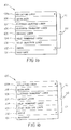
- the OLED device 100 of this invention comprises a transparent substrate 101, a transparent anode 102, a hole-injection layer (HIL) 103, a hole transport layer (HTL) 104, an emissive layer (EML) 105, an electron-transport layer (ETL) 106, an interlayer (IL) 108, and a reflective layer 109a or 109b.
- the interlayer 108 preferably includes a semiconductor metal, metal, metal alloy, or an intermetallic compound disposed over the ultrathin low absorption electron-injecting layer. The interlayer thickness is selected to cause an increase in contrast.
- HIL hole-injection layer
- HTL hole transport layer
- EML emissive layer
- ETL electron-transport layer
- IL interlayer
- the interlayer 108 preferably includes a semiconductor metal, metal, metal alloy, or an intermetallic compound disposed over the ultrathin low absorption electron-injecting layer.
- the interlayer thickness is selected to cause an increase in contrast.
- an electron-injecting layer 107 (hereinafter referred to as the cathode layer) is provided over the ETL layer.
- the reflective layer 109b contains an electron-injecting element that diffuses to the surface of ETL providing electron injection.
- the cathode layer preferably is ultrathin and has a thickness in the range of 0.2 to 10nm.
- the anode and the reflective layer that is in electrical connection to the cathode layer are connected to a voltage source 110 via conductors 111 allowing electrical current through the organic layers, resulting in light emission or electroluminescence from the OLED device.
- the electroluminescence can be viewed from the substrate side.
- the intensity of the electroluminescence is dependent on the magnitude of the electrical current that is passed through the OLED device 100, which in turn is dependent on the luminescent and electrical characteristics of the organic layers as well as the charge-injecting nature of the contacting electrodes.
- composition and the function of the various layers constituting the OLED device are described as follows:
- Substrate 101 may include glass, ceramic, or plastics. Since the OLED device fabrication does not require high temperature process, any substrate that can withstand process temperatures of the order of 100°C is useful, which includes most thermal plastics.
- the substrate may take the form of rigid plate, flexible sheet, or curved surfaces.
- Substrate 101 may include support with electronic backplane, and thus includes active-matrix substrates, which contain electronic addressing and switching elements. Examples of such active-matrix substrates include substrates with high-temperature polysilicon thin-film-transistors, substrates with low-temperature polysilicon thin-film-transistors, substrates with amorphous silicon transistors, or any substrates with thin-film-transistor. Those skilled in the art will appreciate that other circuit elements can be used to address and drive the OLED devices.
- Hole-injecting layer (HIL) 103 provides the function of increasing the efficiency of the hole injection from the anode into the organic layers. It has been shown, for example in US-A-4,885,211, that a porphorinic or phthalocyanine compound is useful as a hole injection layer, resulting in increased luminance efficiency and operational stability.
- HIL materials include CFx which is a fluorinated polymer deposited by plasma-assisted vapor deposition, wherein x is less than or equal to 2 and greater than 0.
- the color of the EL devices can be tuned by using fluorescent dyes of different emission wavelengths in a common host material.
- US-A-4,769,292 has described this dopant scheme in considerable details for OLED devices using Alq as the host material.
- the emissive layer can contain a green light-emitting doped material, a blue light-emitting doped material, or a red light-emitting doped material.
- Preferred host materials include the class of 8-quinolinol metal chelate compounds with the chelating metals being Al, Mg, Li, Zn, for example.
- Another preferred class of host materials includes anthracene derivatives such as 9,10 dinaphthyl anthracene; 9,10 dianthryl anthracene; and alkyl substituted 9,10 dinaphthyl anthracene, as disclosed in US-A-5,935,721.
- Dopant materials include most fluorescent and phorphorescent dyes and pigments.
- Preferred dopant materials include coumarins such as coumarin 6, dicyanomethylenepyrans such as 4-dicyanomethylene-4H pyrans, as disclosed in US-A-4,769,292 and in US-A-6,020,078.
- Electron-transport layer 106 of FIG. 1a provides the function of delivering electrons injected from the cathode layer 107 to the emissive layer 105.
- Useful materials include Alq and benzazoles as disclosed in US-A-5,645,948.
- the cathode layer 107 of FIG. 1a includes an electron-injecting bilayer element such as LiF/Al.
- An electron-injecting bilayer element such as LiF/Al.
- a single-layer of low-work function metal or a low-work function alloy such as Mg:Ag [C.W. Tang and S.A. VanSlyke, Appl. Phys. Lett. 51, 913 (1987)] or a Li doped surface of an electron-transport layer can also provide efficient electron injection [Junji Kido and Toshio Matsumoto, Appl. Phys. Lett. 73, 2866(1998)] to the ETL layer.
- the cathode layer 107 (see FIG. 1a) has a work function between 2 and 4 volts.
- the cathode layers should preferably be of high optical transmittance.
- the interlayer 108 includes electrically conductive semitransparent layers of semimetals, metals, intermetallic compound or alloys thereof such as Ge, Se, Te, GeTe, W, Mo, or Ta.
- the required layer thickness for minimization of reflectivity is usually thin which is beneficial from a fabrication point view.
- the reflective layers 109a of FIG. 1a and 109b of FIG. 1b are preferably highly reflective and conducting. These include metals like Ag, Al, Au, and Cu and alloys having one or more of these metals as a major component.
- the reflective layer 109b of FIG. 1b must additionally contain an electron-injecting dopant capable of resulting in an electron-injecting contact to the ETL layer.
- dopant metals preferably include alkaline and alkaline earth metals but, in any event, should have materials that have a work function between 2 and 4 volts.
- FIG. 1a and FIG. 1b embodiments are believed preferred, it will be appreciated by those skilled in the art that a device can also be made which does not use hole-injection layer 103, hole transport layer 104, and electron-transport layer 106.
- the emissive layer can be selected to include hole-transport and electron-transport functions and the anode layer can function as the hole-injection layer. In such an instance, the device requires emissive layer 105 and does not require layers 103, 104, and 106.
- Table 1 for the appropriate functions of layers corresponding to the listed acronym.
- the substrates used were ITO coated glass upon which the layers comprising the OLEDs were deposited.
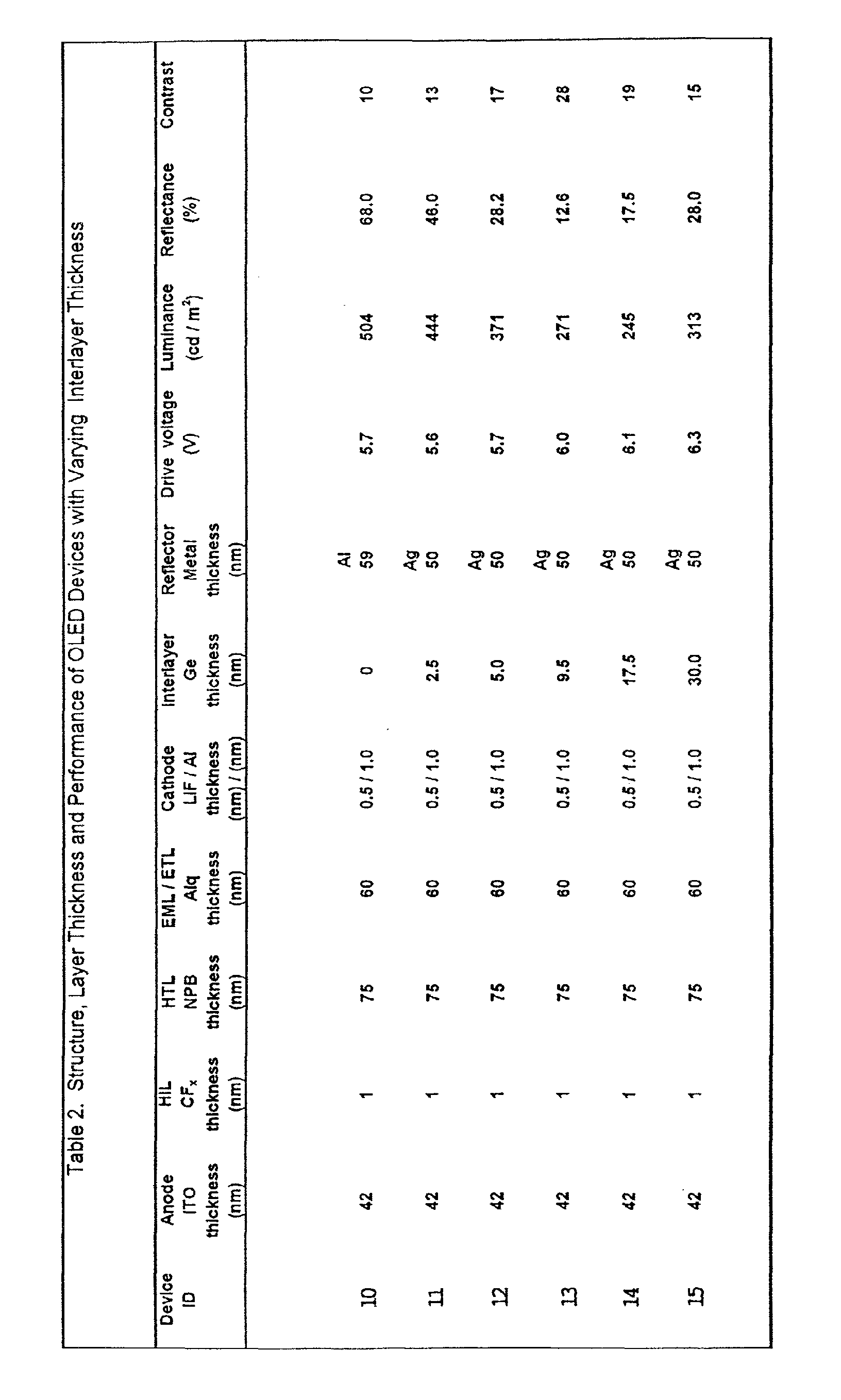
- Tables 2 through 5 presented are the structure, layer thickness, and performance of the devices.
- the HTL and EML/ETL were deposited using a vacuum coater in a single pump-down run. These samples were then transferred to a Plasmatron multifunction deposition system (having the capability of coating by resistive and e-beam heating as well as by sputtering without breaking vacuum) where all the remaining layers were deposited. Finally, the devices were hermetically encapsulated in a glove box filled with dry nitrogen.
- the luminance of the devices was measured using a Photo Research PR 650 spectrophotometer as a function of current.
- the luminance, L (cd/m 2 ), of the devices shown in Tables 2 through 5 refers to that when a current corresponding to 20 mA/cm 2 is driven through the device, and V (volt) is the drive voltage under this condition after accounting for voltage drop due to ITO resistance.
- the reflectivity of the devices was measured through the substrate using Filmetrics F 20, a thin film measurement system. Prior to measurement, the instrument was calibrated using a single crystal Si wafer as a standard. The reflectivity values given in the Tables are for 525 nm, which is approximately the wavelength of Alq emission.
- C (L e + L a R)/ L a R, where L e is the luminance of the device in total darkness, L a is the ambient light intensity and R is the device reflectance.
- the contrast shown are for ambient light intensity of 80 cd/m 2 .
- the device 100 is a standard device having a LiF/Al bilayer cathode comprising an e-beam evaporated Al layer on an ultrathin LiF film. All other devices, 101 through 105 were provided with a Ge interlayer between the ultrathin LiF/Al cathode and the reflective layer.
- the term ultrathin electron-injecting layer refers to an electron-injecting layer 107 (FIG. 1a) having a thickness in a range from 0.2 to 10 nm. Preferably, it has been determined that the range should be from appropriately from 1 to 5 nm.
- the electron-injecting layer 107 should be a low absorption layer, which means that some amount of light must pass through this layer.
- the term low absorption means that the transmittance of the electron-injecting layer 107 should be at least 25% at the wavelength(s) of interest.
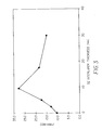
- the reflective layer for these devices was a thermally evaporated layer of Ag. It can be easily seen from Table 2 and FIG. 2 that the device reflectivity, initially decreasing with increasing Ge interlayer thickness, reaches to its minimum value of 12.6 % at about 9.5 nm before increasing with interlayer thickness.
- the interlayer thickness is selected to be between 3 and 30 nm to lower the device reflectivity and increase the contrast. However, as shown in FIG.
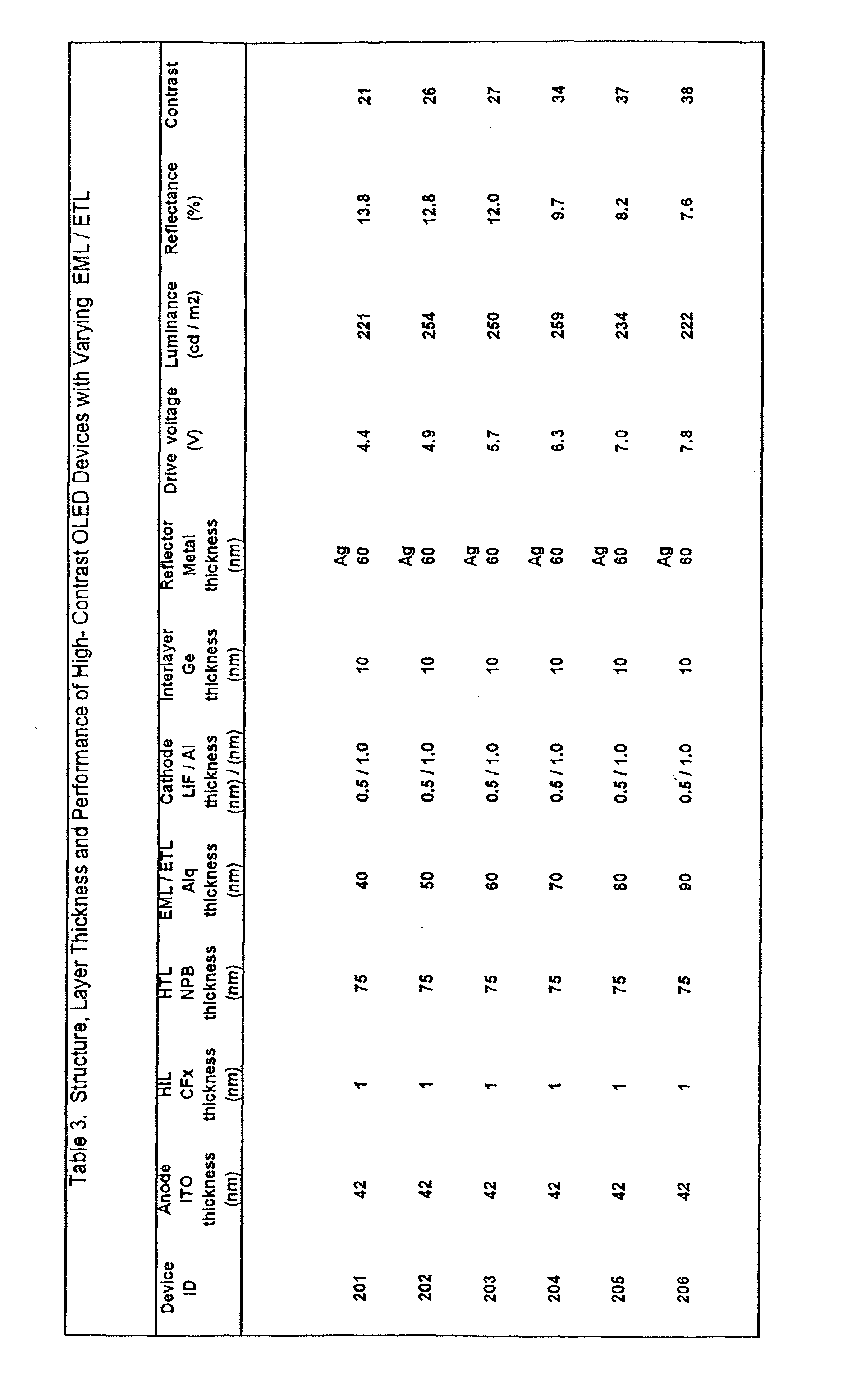
- Table 3 shown are the structure, layer thickness, and performance of a set of devices made in another run.
- the Alq thickness was varied in this set giving rise to devices having different drive voltages.
- All the devices, 201 through 206, were provided with a fixed 10-nm thick Ge interlayer between the ultrathin LiF/Al cathode and a reflective layer.
- the reflective layer for the devices was sputtered from a Ag target. It can easily be seen that the device reflectivity has been lowered significantly by the interlayer. It is also to be noted that the reflectivity is not a strong function of Alq thickness. This implies that the approach is effective for low and high voltage devices although the interlayer thickness has to be selected for maximization of contrast.
- the cathode for the standard device was LiF/Al, bilayer, and those for the high contrast devices were ultrathin LiF/Y bilayers.
- the reflective layer for the device 302 was an e-beam evaporated Al layer, whereas the high-contrast device 303 was provided with sputtered Ag reflective layer.
- the devices 302 and 303 have identical organic and Ge interlayer, but the device 303 having the Ag reflective layer has lower reflectivity and higher contrast compared to device 302 having an Al reflective layer device 302.
- the cathode for a conventional device 401 is a LiF/Al bilayer.
- the Ge interlayer thickness was varied within the series.
- the interlayer was deposited directly on the ETL of devices 402 through 404.
- the cathodes for these devices were formed by sputtering on ETL a silver alloy containing 4-w% Li.
- the drive voltages of these devices are higher than that of the standard devices, presumably due to their relatively inefficient electron injection efficiencies, lower device reflectivity and higher contrast are achieved when the Ge interlayers are incorporated.
- Tables 2 through 5 show the benefit of including a thin interlayer in the OLED structure.
- the drive voltage stayed nearly the same but the reflectivity is reduced significantly resulting in a three-fold increase in contrast.
- the OLED device wherein the interlayer has a thickness selected to be in a range of 3.0 to 30nm.
- the OLED device wherein the interlayer has a thickness selected to be in a range of 3.0 to 30nm.
- the OLED device wherein the reflective layer material is Au, Ag, Cu, Al and alloys thereof.
- the OLED device wherein the reflective layer material is Au, Ag, Cu, Al and alloys thereof.
- the OLED device where in the reflecting layer contains an alkaline or alkaline earth metal.
- the OLED device wherein the electron-injecting layer has a thickness in the range of 0.2 to 10nm.
- the OLED device wherein the electron-injecting layer has a thickness in the range of 0.2 to 10nm.
- the OLED device wherein the electron-injecting layer has a work function between 2 and 4 volt.
- the OLED device wherein the electron-injecting layer has a work function between 2 and 4 volt.
- the OLED device wherein the electron-injecting layer includes a LiF/Al bilayer structure.
- the OLED device wherein the electron-injecting layer includes a LiF/Al bilayer structure.
- the OLED device wherein the electron-injecting layer includes a LiF/Y bilayer structure.
- the OLED device wherein the electron-injecting layer includes a LiF/Y bilayer structure.
- the OLED device wherein the emissive layer contains one or more light emitting doped materials.
Landscapes
- Physics & Mathematics (AREA)
- Optics & Photonics (AREA)
- Electroluminescent Light Sources (AREA)
Abstract
Description
- ITO/NPB/Alq/LiF/Al/85 nm ZnO1-x/Al. This device also exhibited greatly reduced reflectivity relative to a standard device.
| OLED | Organic light-emitting diode |
| ITO | Indium tin oxide |
| HIL | Hole-injection layer |
| HTL | Hole-transport layer |
| EML | Emissive layer |
| ETL | Electron-transport layer |
| NPB | 4,4'-Bis[N-(1-naphthyl)-N-phenylamino]biphenyl (NPB) |
| Alq | Tris(8-hydroxyquinoline) aluminum |
| LiF | Lithium Fluoride |
| Al | Aluminum |
| Y | Yttrium |
| Ge | Germanium |
| Ag | Silver |

- 4,4'-Bis[N-(1-naphthyl)-N-phenylamino]biphenyl (NPB)
- 4,4"-Bis[N-(1-naphthyl)-N-phenylamino]-p-terphenyl
- 4,4'-Bis[N-(2-naphthyl)-N-phenylamino]biphenyl
- 1,5-Bis[N-(1-naphthyl)-N-phenylamino]naphthalene
- 4,4'-Bis[N-(2-pyrenyl)-N-phenylamino]bi-phenyl
- 4,4'-Bis[N-(2-perylenyl)-N-phenylamino]biphenyl
- 2,6-Bis(di-p-tolylamino)naphthalene
- 2,6-Bis[di-(1-naphtyl)amino]naphthalene


Claims (10)
- An OLED device for providing increased contrast, comprising:a) a transparent substrate;b) an anode formed of a transparent conductive material over the substrate;c) an emissive layer having an electroluminescent material provided over the anode layer;d) an ultrathin low absorption electron-injecting layer laid over the electron-transport layer;e) an interlayer including a semi-metal, metal, metal alloy or an intermetallic compound disposed over the ultrathin low absorption electron-injecting layer;f) a layer of reflective material provided over the interlayer; andg) wherein the interlayer thickness is selected to cause an increase in contrast.
- An OLED device for providing increased contrast, comprising:a) a transparent substrate;b) an anode formed of a transparent conductive material over the substrate;c) hole-injection and hole-transport layers respectively formed over the anode;d) an emissive layer formed over the hole-transport layer and including an electroluminescent material;e) an electron-transport layer formed over the emissive layer;f) an ultrathin low absorption electron-injecting layer laid over the electron-transport layer;g) an interlayer including a semi-metal, metal, metal alloy or an intermetallic compound disposed over the ultrathin low-absorption electron-injecting layer;h) a layer of reflective material provided over the interlayer; andi) wherein the interlayer thickness is selected to cause an increase in contrast.
- An OLED device for providing increased contrast, comprising:a) a transparent substrate;b) an anode formed of a transparent conductive material over the substrate;c) an emissive layer formed over the substrate and including an electroluminescent material;d) an interlayer provided over the emissive layer including a semi-metal, metal, metal alloy or an intermetallic compound;e) a layer of reflective material provided over the interlayer; andf) wherein the reflective layer is doped with an electron-injecting dopant which migrates sufficiently to provide an electron-injecting connection between the reflecting layer and the emissive layer and wherein the interlayer thickness is selected to cause an increase in contrast.
- An OLED device for providing increased contrast, comprising:a) a transparent substrate;b) an anode formed of a transparent conductive material over the substrate;c) hole injection and hole-transport layers respectively formed over the anode;d) an emissive layer formed over the hole-injecting layer and including an electroluminescent material;e) an electron-transport layer formed over the emissive layer;f) an interlayer including a semi-metal, metal, metal alloy or an intermetallic compound disposed between the reflective layer and the electron-transport layer;g) a layer of reflective material provided over the interlayer; andh) wherein the reflective layer is doped with an electron-injecting dopant which migrates sufficiently to provide an electron-injecting connection between the reflecting layer and the transport layer and wherein the interlayer thickness is selected to cause an increase in contrast.
- The OLED device of claim 1 wherein the interlayer includes Ge, Se, Te, GeTe, W, Mo, Ta or alloys thereof.
- The OLED device of claim 2 wherein the interlayer includes Ge, Se, Te, GeTe, W, Mo, Ta or alloys thereof.
- The OLED device of claim 3 wherein the interlayer includes Ge, Se, Te, GeTe, W, Mo, Ta or alloys thereof.
- The OLED device of claim 1 wherein the interlayer has a thickness selected to be in a range of 3.0 to 30nm.
- A method of making an OLED device for providing increased contrast, comprising the steps of:a) providing a transparent substrate and a spaced reflective layer;b) providing an anode formed of a transparent conductive material over the substrate;c) providing an emissive layer having an electroluminescent material provided over the anode layer;d) providing an interlayer between the reflective layer and the emissive layer, such interlayer includes a semi-metal, metal, metal alloy or an intermetallic compound; ande) providing electron injection to the emissive layer by depositing an ultrathin electron-injecting layer between the interlayer and the emissive layer or by providing dopant, including an alkaline or alkaline earth metal, in the reflective layer which migrates sufficiently to provide an electron-injecting connection between the reflecting layer and the emissive layer.
- An OLED device comprising:a) a transparent substrate;b) an anode formed of a conductive material over the substrate;c) an emissive layer having an electroluminescent material provided over the anode; andd) either an ultrathin cathode over the emissive layer, a thin interlayer over the ultrathin cathode and a reflecting layer over the thin interlayer or a thin interlayer over the emissive layer and a reflecting layer containing an electron-injecting dopant over the thin interlayer.
Applications Claiming Priority (2)
| Application Number | Priority Date | Filing Date | Title |
|---|---|---|---|
| US09/852,956 US6558820B2 (en) | 2001-05-10 | 2001-05-10 | High contrast light-emitting diode devices |
| US852956 | 2001-05-10 |
Publications (2)
| Publication Number | Publication Date |
|---|---|
| EP1256990A2 true EP1256990A2 (en) | 2002-11-13 |
| EP1256990A3 EP1256990A3 (en) | 2006-10-18 |
Family
ID=25314644
Family Applications (1)
| Application Number | Title | Priority Date | Filing Date |
|---|---|---|---|
| EP02076723A Withdrawn EP1256990A3 (en) | 2001-05-10 | 2002-04-29 | High contrast light-emitting diode devices |
Country Status (5)
| Country | Link |
|---|---|
| US (1) | US6558820B2 (en) |
| EP (1) | EP1256990A3 (en) |
| JP (1) | JP2002343573A (en) |
| KR (1) | KR20020086281A (en) |
| TW (1) | TW552721B (en) |
Cited By (2)
| Publication number | Priority date | Publication date | Assignee | Title |
|---|---|---|---|---|
| WO2004053018A1 (en) * | 2002-12-06 | 2004-06-24 | Shuang Xie | Electroluminescent devices |
| CN101840993A (en) * | 2010-05-05 | 2010-09-22 | 北京科技大学 | Multilayer film structure having exchange bias effect and manufacturing method thereof |
Families Citing this family (49)
| Publication number | Priority date | Publication date | Assignee | Title |
|---|---|---|---|---|
| US6623870B1 (en) * | 1996-08-02 | 2003-09-23 | The Ohio State University | Electroluminescence in light emitting polymers featuring deaggregated polymers |
| GB2389752B (en) * | 1999-05-28 | 2004-02-25 | Nec Corp | Mobile telecommunications system |
| JP4053260B2 (en) * | 2000-10-18 | 2008-02-27 | シャープ株式会社 | Organic electroluminescence display element |
| EP1423991A4 (en) * | 2001-07-27 | 2009-06-17 | Univ Ohio State | METHOD FOR PRODUCING POLYMER LIGHT EMISSION ELEMENTS BY LAMINATION |
| SG114514A1 (en) * | 2001-11-28 | 2005-09-28 | Univ Singapore | Organic light emitting diode (oled) |
| CA2419121A1 (en) * | 2002-05-03 | 2003-11-03 | Luxell Technologies, Inc. | Dark layer for an electroluminescent device |
| AUPS327002A0 (en) * | 2002-06-28 | 2002-07-18 | Kabay & Company Pty Ltd | An electroluminescent light emitting device |
| US7038373B2 (en) * | 2002-07-16 | 2006-05-02 | Eastman Kodak Company | Organic light emitting diode display |
| US7015640B2 (en) * | 2002-09-11 | 2006-03-21 | General Electric Company | Diffusion barrier coatings having graded compositions and devices incorporating the same |
| JP3706605B2 (en) * | 2002-09-27 | 2005-10-12 | 三洋電機株式会社 | Organic electroluminescence device and method for manufacturing the same |
| WO2004082338A1 (en) * | 2003-03-13 | 2004-09-23 | Fujitsu Limited | Organic electroluminescence device and organic electroluminescence display |
| US6790594B1 (en) * | 2003-03-20 | 2004-09-14 | Eastman Kodak Company | High absorption donor substrate coatable with organic layer(s) transferrable in response to incident laser light |
| JP3877692B2 (en) * | 2003-03-28 | 2007-02-07 | 三洋電機株式会社 | Organic electroluminescence device and method for manufacturing the same |
| US20040256978A1 (en) * | 2003-05-27 | 2004-12-23 | Gang Yu | Array comprising organic electronic devices with a black lattice and process for forming the same |
| US7045954B2 (en) * | 2003-06-17 | 2006-05-16 | City University Of Hong Kong | Organic light-emitting device with reduction of ambient-light-reflection by disposing a multilayer structure over a semi-transparent cathode |
| US20040263064A1 (en) * | 2003-06-24 | 2004-12-30 | Cheng-Wen Huang | Integrated double-sided organic light-emitting display |
| JP2005063838A (en) * | 2003-08-13 | 2005-03-10 | Toshiba Matsushita Display Technology Co Ltd | Optical device and organic EL display device |
| TWI251712B (en) * | 2003-08-15 | 2006-03-21 | Prime View Int Corp Ltd | Interference display plate |
| TW593127B (en) | 2003-08-18 | 2004-06-21 | Prime View Int Co Ltd | Interference display plate and manufacturing method thereof |
| US20050052119A1 (en) * | 2003-09-08 | 2005-03-10 | Gang Yu | Organic electronic device having low background luminescence |
| GB0329364D0 (en) * | 2003-12-19 | 2004-01-21 | Cambridge Display Tech Ltd | Optical device |
| JP4090447B2 (en) * | 2004-03-29 | 2008-05-28 | 三洋電機株式会社 | Organic electroluminescence device |
| TWI231723B (en) * | 2004-04-16 | 2005-04-21 | Ind Tech Res Inst | Organic electroluminescence display device |
| JP2008500695A (en) * | 2004-05-25 | 2008-01-10 | エージェンシー・フォア・サイエンス・テクノロジー・アンド・リサーチ | Composite optical breakdown electrode for high-contrast electroluminescent devices |
| US7365486B2 (en) * | 2004-07-09 | 2008-04-29 | Au Optronics Corporation | High contrast organic light emitting device with electron transport layer including fullerenes |
| US8124434B2 (en) | 2004-09-27 | 2012-02-28 | Qualcomm Mems Technologies, Inc. | Method and system for packaging a display |
| US7424198B2 (en) | 2004-09-27 | 2008-09-09 | Idc, Llc | Method and device for packaging a substrate |
| US7446926B2 (en) | 2004-09-27 | 2008-11-04 | Idc, Llc | System and method of providing a regenerating protective coating in a MEMS device |
| US7184202B2 (en) * | 2004-09-27 | 2007-02-27 | Idc, Llc | Method and system for packaging a MEMS device |
| US7368803B2 (en) | 2004-09-27 | 2008-05-06 | Idc, Llc | System and method for protecting microelectromechanical systems array using back-plate with non-flat portion |
| US7405924B2 (en) | 2004-09-27 | 2008-07-29 | Idc, Llc | System and method for protecting microelectromechanical systems array using structurally reinforced back-plate |
| US7573547B2 (en) | 2004-09-27 | 2009-08-11 | Idc, Llc | System and method for protecting micro-structure of display array using spacers in gap within display device |
| US7668415B2 (en) * | 2004-09-27 | 2010-02-23 | Qualcomm Mems Technologies, Inc. | Method and device for providing electronic circuitry on a backplate |
| US7701631B2 (en) | 2004-09-27 | 2010-04-20 | Qualcomm Mems Technologies, Inc. | Device having patterned spacers for backplates and method of making the same |
| US20060138946A1 (en) * | 2004-12-29 | 2006-06-29 | Jian Wang | Electrical device with a low reflectivity layer |
| US7554112B1 (en) | 2005-03-10 | 2009-06-30 | E. I. Du Pont De Nemours And Company | Organic electronic device and processes for forming and using the same |
| US8548974B2 (en) * | 2005-07-25 | 2013-10-01 | The Boeing Company | Apparatus and methods for providing geographically oriented internet search results to mobile users |
| US20070138637A1 (en) * | 2005-12-19 | 2007-06-21 | Shiva Prakash | Electronic device having low background luminescence, a black layer, or any combination thereof |
| WO2007120885A2 (en) * | 2006-04-13 | 2007-10-25 | Qualcomm Mems Technologies, Inc. | Mems devices and processes for packaging such devices |
| JP5109303B2 (en) | 2006-07-31 | 2012-12-26 | ソニー株式会社 | Organic light emitting device and display device |
| KR100874472B1 (en) * | 2007-02-28 | 2008-12-18 | 에스에프씨 주식회사 | Blue light emitting compound and organic light emitting device using the same |
| CN101533850B (en) * | 2008-03-13 | 2012-07-04 | 奇美电子股份有限公司 | Organic light emitting diode display device and display system thereof |
| US20090323170A1 (en) * | 2008-06-30 | 2009-12-31 | Qualcomm Mems Technologies, Inc. | Groove on cover plate or substrate |
| US8643000B2 (en) * | 2008-11-18 | 2014-02-04 | E I Du Pont De Nemours And Company | Organic electronic device with low-reflectance electrode |
| DE102009012346B4 (en) * | 2009-03-09 | 2024-02-15 | Merck Patent Gmbh | Organic electroluminescent device and method for producing the same |
| US8379392B2 (en) | 2009-10-23 | 2013-02-19 | Qualcomm Mems Technologies, Inc. | Light-based sealing and device packaging |
| CN103151468B (en) * | 2013-03-07 | 2015-08-19 | 深圳市华星光电技术有限公司 | A kind of Organic Light Emitting Diode and preparation method thereof, display unit |
| KR102392914B1 (en) * | 2020-08-24 | 2022-04-29 | 고려대학교 산학협력단 | Electrode and organic light emitting device using the electrode |
| CN112038457B (en) * | 2020-09-11 | 2021-10-29 | 扬州乾照光电有限公司 | A flip-chip red LED chip and method of making the same |
Family Cites Families (13)
| Publication number | Priority date | Publication date | Assignee | Title |
|---|---|---|---|---|
| US4287449A (en) * | 1978-02-03 | 1981-09-01 | Sharp Kabushiki Kaisha | Light-absorption film for rear electrodes of electroluminescent display panel |
| US4720432A (en) | 1987-02-11 | 1988-01-19 | Eastman Kodak Company | Electroluminescent device with organic luminescent medium |
| US4885211A (en) | 1987-02-11 | 1989-12-05 | Eastman Kodak Company | Electroluminescent device with improved cathode |
| US4769292A (en) | 1987-03-02 | 1988-09-06 | Eastman Kodak Company | Electroluminescent device with modified thin film luminescent zone |
| US5645948A (en) | 1996-08-20 | 1997-07-08 | Eastman Kodak Company | Blue organic electroluminescent devices |
| US5917280A (en) * | 1997-02-03 | 1999-06-29 | The Trustees Of Princeton University | Stacked organic light emitting devices |
| US6307528B1 (en) * | 1997-12-08 | 2001-10-23 | Hughes Electronics Corporation | Contrast organic light-emitting display |
| US5935721A (en) | 1998-03-20 | 1999-08-10 | Eastman Kodak Company | Organic electroluminescent elements for stable electroluminescent |
| KR100267054B1 (en) * | 1998-04-22 | 2000-09-15 | 김선욱 | Organic light-emitting device having an improved contrast ratio |
| US6140763A (en) * | 1998-07-28 | 2000-10-31 | Eastman Kodak Company | Interfacial electron-injecting layer formed from a doped cathode for organic light-emitting structure |
| GB9901334D0 (en) * | 1998-12-08 | 1999-03-10 | Cambridge Display Tech Ltd | Display devices |
| US6020078A (en) | 1998-12-18 | 2000-02-01 | Eastman Kodak Company | Green organic electroluminescent devices |
| US6278236B1 (en) * | 1999-09-02 | 2001-08-21 | Eastman Kodak Company | Organic electroluminescent devices with electron-injecting layer having aluminum and alkali halide |
-
2001
- 2001-05-10 US US09/852,956 patent/US6558820B2/en not_active Expired - Lifetime
-
2002
- 2002-03-25 TW TW091105739A patent/TW552721B/en not_active IP Right Cessation
- 2002-04-29 EP EP02076723A patent/EP1256990A3/en not_active Withdrawn
- 2002-05-08 JP JP2002132910A patent/JP2002343573A/en not_active Withdrawn
- 2002-05-09 KR KR1020020025641A patent/KR20020086281A/en not_active Ceased
Cited By (3)
| Publication number | Priority date | Publication date | Assignee | Title |
|---|---|---|---|---|
| WO2004053018A1 (en) * | 2002-12-06 | 2004-06-24 | Shuang Xie | Electroluminescent devices |
| CN101840993A (en) * | 2010-05-05 | 2010-09-22 | 北京科技大学 | Multilayer film structure having exchange bias effect and manufacturing method thereof |
| CN101840993B (en) * | 2010-05-05 | 2012-02-15 | 北京科技大学 | Multilayer film structure having exchange bias effect and manufacturing method thereof |
Also Published As
| Publication number | Publication date |
|---|---|
| TW552721B (en) | 2003-09-11 |
| KR20020086281A (en) | 2002-11-18 |
| JP2002343573A (en) | 2002-11-29 |
| US20030035978A1 (en) | 2003-02-20 |
| EP1256990A3 (en) | 2006-10-18 |
| US6558820B2 (en) | 2003-05-06 |
Similar Documents
| Publication | Publication Date | Title |
|---|---|---|
| US6558820B2 (en) | High contrast light-emitting diode devices | |
| US7309956B2 (en) | Top-emitting OLED device with improved-off axis viewing performance | |
| KR101094737B1 (en) | Excellent organic light emitting device | |
| US7002293B2 (en) | Organic light emitting diode with improved light emission through the cathode | |
| EP1670084B1 (en) | Organic light emitting display and method for fabricating the same | |
| US7049741B2 (en) | Organic light emitting diode with improved light emission through substrate | |
| US6469437B1 (en) | Highly transparent organic light emitting device employing a non-metallic cathode | |
| US5998803A (en) | Organic light emitting device containing a hole injection enhancement layer | |
| US6551725B2 (en) | Inorganic buffer structure for organic light-emitting diode devices | |
| CA2514506C (en) | Oleds having inorganic material containing anode capping layer | |
| EP1076368A2 (en) | A surface-emitting organic light-emitting diode | |
| US6797129B2 (en) | Organic light-emitting device structure using metal cathode sputtering | |
| US20040140758A1 (en) | Organic light emitting device (OLED) display with improved light emission using a metallic anode | |
| EP0856896B1 (en) | Light emitting diodes | |
| EP1256989B1 (en) | Organic light emitting diode with high contrast ratio | |
| US20030129447A1 (en) | Sputtered cathode having a heavy alkaline metal halide-in an organic light-emitting device structure | |
| US20070222371A1 (en) | Top-emitting OLED device with improved stability | |
| US20030224204A1 (en) | Sputtered cathode for an organic light-emitting device having an alkali metal compound in the device structure | |
| EP1227528A2 (en) | Organic light emitting devices having a modified electron-transport layer | |
| JP2001060495A (en) | Organic EL device | |
| JP2001118681A (en) | Organic el element and its method of driving | |
| JPH09283281A (en) | Organic electroluminescent device | |
| Burrows et al. | Organic light-emitting devices for ultralightweight color flat panel displays | |
| JP2000268972A (en) | Organic el element |
Legal Events
| Date | Code | Title | Description |
|---|---|---|---|
| PUAI | Public reference made under article 153(3) epc to a published international application that has entered the european phase |
Free format text: ORIGINAL CODE: 0009012 |
|
| AK | Designated contracting states |
Kind code of ref document: A2 Designated state(s): AT BE CH CY DE DK ES FI FR GB GR IE IT LI LU MC NL PT SE TR |
|
| AX | Request for extension of the european patent |
Free format text: AL;LT;LV;MK;RO;SI |
|
| PUAL | Search report despatched |
Free format text: ORIGINAL CODE: 0009013 |
|
| AK | Designated contracting states |
Kind code of ref document: A3 Designated state(s): AT BE CH CY DE DK ES FI FR GB GR IE IT LI LU MC NL PT SE TR |
|
| AX | Request for extension of the european patent |
Extension state: AL LT LV MK RO SI |
|
| AKX | Designation fees paid | ||
| REG | Reference to a national code |
Ref country code: DE Ref legal event code: 8566 |
|
| STAA | Information on the status of an ep patent application or granted ep patent |
Free format text: STATUS: THE APPLICATION IS DEEMED TO BE WITHDRAWN |
|
| 18D | Application deemed to be withdrawn |
Effective date: 20071029 |