EP1255333A1 - Current generator circuit and method of providing drive current to a laser diode driver - Google Patents
Current generator circuit and method of providing drive current to a laser diode driver Download PDFInfo
- Publication number
- EP1255333A1 EP1255333A1 EP01303927A EP01303927A EP1255333A1 EP 1255333 A1 EP1255333 A1 EP 1255333A1 EP 01303927 A EP01303927 A EP 01303927A EP 01303927 A EP01303927 A EP 01303927A EP 1255333 A1 EP1255333 A1 EP 1255333A1
- Authority
- EP
- European Patent Office
- Prior art keywords
- current
- base
- mirror
- transistor
- circuit
- Prior art date
- Legal status (The legal status is an assumption and is not a legal conclusion. Google has not performed a legal analysis and makes no representation as to the accuracy of the status listed.)
- Granted
Links
- 238000000034 method Methods 0.000 title claims description 8
- 230000008033 biological extinction Effects 0.000 claims abstract description 9
- 229910000577 Silicon-germanium Inorganic materials 0.000 claims abstract description 6
- LEVVHYCKPQWKOP-UHFFFAOYSA-N [Si].[Ge] Chemical compound [Si].[Ge] LEVVHYCKPQWKOP-UHFFFAOYSA-N 0.000 claims abstract description 4
- 238000005516 engineering process Methods 0.000 claims abstract description 4
- 230000008878 coupling Effects 0.000 claims description 4
- 238000010168 coupling process Methods 0.000 claims description 4
- 238000005859 coupling reaction Methods 0.000 claims description 4
- 239000004065 semiconductor Substances 0.000 claims description 2
- 238000010586 diagram Methods 0.000 description 3
- 230000015556 catabolic process Effects 0.000 description 2
- 238000006731 degradation reaction Methods 0.000 description 2
- 230000000694 effects Effects 0.000 description 2
- 230000006641 stabilisation Effects 0.000 description 2
- 230000003321 amplification Effects 0.000 description 1
- 230000008859 change Effects 0.000 description 1
- 230000000295 complement effect Effects 0.000 description 1
- 238000010276 construction Methods 0.000 description 1
- 230000006872 improvement Effects 0.000 description 1
- 230000007246 mechanism Effects 0.000 description 1
- 230000004048 modification Effects 0.000 description 1
- 238000012986 modification Methods 0.000 description 1
- 238000003199 nucleic acid amplification method Methods 0.000 description 1
- 230000008569 process Effects 0.000 description 1
- 230000007704 transition Effects 0.000 description 1
Images


Classifications
-
- H—ELECTRICITY
- H01—ELECTRIC ELEMENTS
- H01S—DEVICES USING THE PROCESS OF LIGHT AMPLIFICATION BY STIMULATED EMISSION OF RADIATION [LASER] TO AMPLIFY OR GENERATE LIGHT; DEVICES USING STIMULATED EMISSION OF ELECTROMAGNETIC RADIATION IN WAVE RANGES OTHER THAN OPTICAL
- H01S5/00—Semiconductor lasers
- H01S5/04—Processes or apparatus for excitation, e.g. pumping, e.g. by electron beams
- H01S5/042—Electrical excitation ; Circuits therefor
-
- G—PHYSICS
- G05—CONTROLLING; REGULATING
- G05F—SYSTEMS FOR REGULATING ELECTRIC OR MAGNETIC VARIABLES
- G05F3/00—Non-retroactive systems for regulating electric variables by using an uncontrolled element, or an uncontrolled combination of elements, such element or such combination having self-regulating properties
- G05F3/02—Regulating voltage or current
- G05F3/08—Regulating voltage or current wherein the variable is DC
- G05F3/10—Regulating voltage or current wherein the variable is DC using uncontrolled devices with non-linear characteristics
- G05F3/16—Regulating voltage or current wherein the variable is DC using uncontrolled devices with non-linear characteristics being semiconductor devices
- G05F3/20—Regulating voltage or current wherein the variable is DC using uncontrolled devices with non-linear characteristics being semiconductor devices using diode- transistor combinations
- G05F3/26—Current mirrors
- G05F3/265—Current mirrors using bipolar transistors only
-
- H—ELECTRICITY
- H01—ELECTRIC ELEMENTS
- H01S—DEVICES USING THE PROCESS OF LIGHT AMPLIFICATION BY STIMULATED EMISSION OF RADIATION [LASER] TO AMPLIFY OR GENERATE LIGHT; DEVICES USING STIMULATED EMISSION OF ELECTROMAGNETIC RADIATION IN WAVE RANGES OTHER THAN OPTICAL
- H01S5/00—Semiconductor lasers
- H01S5/04—Processes or apparatus for excitation, e.g. pumping, e.g. by electron beams
- H01S5/042—Electrical excitation ; Circuits therefor
- H01S5/0427—Electrical excitation ; Circuits therefor for applying modulation to the laser
Definitions
- This invention relates, in general, to current generator stabilisation circuits and is particularly, but not exclusively, applicable to laser driver circuits operating in voltage environments having restricted voltage headroom.
- the extinction ratio is the current ratio between a first current yielding a light level attributed to a logical zero value and a second current yielding a light level attributed to a logical one value.
- ac modulation current to the laser diode that provides a logic level control mechanism through which transitions between logical states are controlled, the ac modulation current defined between the first current and the second current. Typical extinction ratios are between about 10:1 or 20:1.
- lasing operation will not commence before a minimum current threshold (I thres ) has been surpassed and that logical zero is defined by a current greater than I thres .
- laser diode operation (having regard to the ac modulation current range) varies as a function of temperature.
- UK Patent application 2 335 556 describes an emitter-follower arrangement in a BiMOS switched current source for a digital to analog converter (DAC) or phase lock loop (PLL) charge pump.
- DAC digital to analog converter
- PLL phase lock loop
- transistor current mirror compensation techniques deployment multiple transistors require voltage headroom that may exceed the inherent capabilities of the supply voltage V cc , with this particularly true in the context of silicon-germanium (SiGe) transistors where there is a trend to increased base-emitter junctions voltages, V be . While the current base problem is most noticeable in pnp structures, npn structures are nevertheless susceptible.
- a current mirror circuit of a laser driver circuit comprising: first and second mirror transistors each having a base electrode and an emitter electrode; first and second emitter resistors coupled, respectively, to the emitter electrodes of the first and second mirror transistors, and characterised by: a resistive element coupled between said base electrodes such that, in use, base leakage current to the first transistor from a current supply causes a voltage drop across the resistive element, wherein the voltage drop acts to boost a voltage through the emitter resistor of the second mirror transistor, thereby to boost, in use, output current provided by the second mirror transistor to the laser driver circuit.
- a method of providing drive current in a laser diode circuit comprising: providing an input current to an input stage of a current mirror, the input current provided to a collector electrode of a first transistor; and characterised by: coupling together base electrodes of the first transistor and a second transistor of an output stage of the current mirror, the coupling occurring through a resistive element arranged to cause generation of a voltage drop across the resistive element; and modulating an output current from the output stage of the current mirror, the output current boosted by the voltage drop across the resistive element to provide the drive current.
- the output current provides current to a current modulator arranged to control an extinction ratio associated with operation of a laser diode.
- a resistive beta compensation current mirror arranged to boost output current supplied to a laser diode having an operational power supply that is less than about 5 volts.
- Another aspect of the present invention provides use of a resistive beta compensation current mirror to boost output current supplied to a laser diode having an operational power supply that is less than about 5 volts, the laser diode preferably supported by a silicon-germanium bipolar transistor semiconductor technology.
- a current mirror circuit connectable, in use, to a laser driver circuit, the current mirror circuit comprising: first and second mirror transistors each having a base electrode and an emitter electrode; first and second emitter. resistors coupled, respectively, to the emitter electrodes of the first and second mirror transistors, and characterised by: a resistive element coupled between said base electrodes such that, in use, base leakage current to the first transistor from a current supply causes a voltage drop across the resistive element, wherein the voltage drop acts to boost a voltage through the emitter resistor of the second mirror transistor, thereby to boost, in use, output current provided by the second mirror transistor to the laser diode circuit.
- the present invention applies resistive beta compensation mirrors to control accurately, for example, laser diodes operating from relatively low supply voltages.
- the present invention therefore provides an improvement in stabilisation of a current generator output employing a current mirror in a low supply voltage environment, especially in a laser driver circuit environment.
- FIGs. 1 and 2 that place the requirements for accurate control of the extinction ratio (FIG. 1) in the context of a laser diode driver circuit (FIG. 3) having an associated current generator circuit (FIG. 2).
- a current supply I in 24 provides current base electrode 26 of emitter-follower transistor 28.
- the current generator circuit 20 in the context of a laser diode driver circuit, therefore acts as a current source. (These current sources may be modulated or may be controlled via analogue or digital control loops).
- a collector electrode 30 of the emitter-follower transistor 28 (in the current generator circuit 20) is coupled to receive voltage supply V cc 29, whilst the emitter electrode is coupled to a common circuit node 32 between base electrodes of first 34 and second 36 mirror transistors.
- a collector electrode 38 of first mirror transistor 34 is also coupled to the base electrode 26 of emitter-follower transistor 28.
- An emitter electrode 40 of the first 34 mirror transistor is coupled to a first resistor 42 that is in parallel with a second resistor 44 further coupled to an emitter 46 of the second 36 mirror transistor. Terminals of the first resistor 42 and the second resistor 44 remote to the first 34 and second 36 mirror transistors are coupled to a reference plane 48, typically ground potential.
- the collector electrode 50 of second mirror transistor 36 provides output current I out 52 to a laser diode driver circuit 60 of FIG. 3.
- the laser diode circuit 60 is a schematic representation showing only the principal components.
- the laser diode driver circuit 60 is coupled to receive output current I out 52 from the collector electrode 50 of second mirror transistor 36 (of FIG. 1). More specifically, in a conventional implementation, ac and dc drive current (corresponding to current output I out 52) is respectively supplied by a pair of current generator circuits 20, each current generator circuit 20 potentially set up in a different way through selection of differing component values.
- ac modulation current I ac feeds a mirrored-pair of transistors 64, one of which is coupled to a laser diode 66 typically implemented externally to the laser driver as a discrete transistor outline (TO) package.
- TO discrete transistor outline
- the dc current source 62 is coupled to a point between the mirrored-pair of transistors 64 and the laser diode 66, as will be understood.
- the laser diode 66, the laser driver 60 and current sources are coupled between a supply potential 68 and a reference plane (not shown), e.g. ground potential.
- FIG. 4 is a diagram of a current generator circuit 100 according to a preferred embodiment of the present invention.
- the emitter-follower transistor 28 in the current mirror
- the current supply I in 24 is provided to the collector electrode 38 of first mirror transistor 34 and a circuit node 104 between the base of second mirror transistor 36 and mirror base resistor (R 1 ) 102.
- Emitter degradation resistors R 2 and R 3 that correspond to first and second resistors 42 and 44 of FIG. 2) act to stabilise voltage effects.
- mirror base resistor (R 1 ) 102 is shown in single component form, it will be understood that the mirror base resistor 102 can be realised by a combination of serial and parallel resistances between the current supply I in 24 and the base of the second mirror transistor 36. Voltage supply V cc 29 is provided to circuit node 104. The emitter degradation resistors R 2 and R 3 are further coupled to a suitable reference plane 106, which may be ground potential
- the circuit of the preferred embodiment effectively increases the operating voltage and hence the voltage headroom derived from the supply voltage V cc .
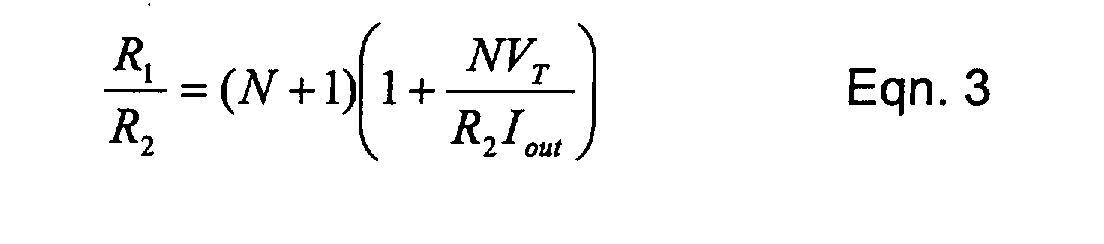
- Eqn. 2 and Eqn. 3 can be further refined to optimise the value of R 1 for a given output current I out at a stated temperature:
- Eqn. 3 it is possible to set the extinction ratio very accurately for low supply voltages Eqn. 3 is therefore used to correct for low gain at a low and substantially fixed I base R 1 voltage drop at a substantially fixed temperature and with a substantially fixed voltage supply.
- FIG. 5 is identical to FIG. 4, although an output side of the current mirror has successive electrically coupled current mirror (amplification) stages comprised from base-coupled transistors T x , T y having emitter electrodes tied to the reference plane 106 through parallel emitter resistors R 3 , R x , R y . Collector electrodes of base-coupled transistors T x , T y are summed to provide the output current I out 52. Emitters from the base coupled transistors T x , T y may be coupled together to facilitate ease in circuit topology. The values of R 3 , R x , R y may be dissimilar so as to change the respective gains of each stage.
- FIG. 6 is a further embodiment of the present invention showing serial cascading of npn and pnp current mirrors.
- an npn-current mirror 100 of the preferred embodiment (as described in FIG. 4) has a gain 1: N .
- Serially cascading the collector electrode of second mirror transistor 36 to a complementary pnp-current mirror 120 having a gain of 1: M provides an overall current gain as the product MN.
- Serial cascading may occur through ancillary circuit components that will be readily appreciated by the skilled address, the serial components omitted for clarity but represented by the dashed lines 122 and 124.
- a base resistor 126 couples together base electrodes of an input transistor 128 and an output transistor 130.
- the collector electrode of second mirror transistor 36 is coupled to both the collector of the input transistor 128 and the base of output transistor 130.
- Emitter electrodes of the pnp-current mirror 120 are coupled to a reference potential via resistive elements 132 and 134 having suitably selected component values.
Landscapes
- Engineering & Computer Science (AREA)
- Physics & Mathematics (AREA)
- Microelectronics & Electronic Packaging (AREA)
- Electromagnetism (AREA)
- General Physics & Mathematics (AREA)
- Nonlinear Science (AREA)
- Radar, Positioning & Navigation (AREA)
- Automation & Control Theory (AREA)
- Condensed Matter Physics & Semiconductors (AREA)
- Optics & Photonics (AREA)
- Semiconductor Lasers (AREA)
Abstract
Description
where k is the Boltzmann's constant voltage across resistor R3, q is charge and T is the absolute temperature (e.g. VT≈twenty-six millivolts (26mV) at two hundred and ninety-three Kelvin (293K)), the voltage drop IbaseR1 is large and the relative resistances can be expressed as:
Claims (12)
- A current mirror circuit (20) of a laser driver circuit (60), the current mirror circuit comprising:first and second mirror transistors (34, 36) each having a base electrode and an emitter electrode;first and second emitter resistors (R2, R3) coupled, respectively, to the emitter electrodes of the first and second mirror transistors, and characterised by:a resistive element (R1, 102) coupled between said base electrodes such that, in use, base leakage current (Ibase) to the first transistor (34) from a current supply (Iin, 24) causes a voltage drop (IbaseR1) across the resistive element (R1, 102), wherein the voltage drop (IbaseR1) acts to boost a voltage through the emitter resistor (R3) of the second mirror transistor (36), thereby to boost, in use, output current (Iout, 52) provided by the second mirror transistor (36) to the laser driver circuit (60).
- The current mirror circuit of claim 1, further comprising at least one further current mirror output stage having a third transistor (Tx, Ty) with a base electrode, an emitter electrode and an associated emitter resistor (Rx, Ry), said third transistor of the at least one further current mirror output stage having its base coupled to the base of the second transistor (36).
- The current mirror circuit of claim 2, wherein emitter electrodes of the second transistor (36) and the third transistor (Tx, Ty) are coupled together.
- The current mirror circuit of claim 1, 2 or 3, wherein said emitter resistors are coupled to a common reference plane (106).
- The current mirror circuit of any preceding claim, wherein the emitter resistors (R2, R3, Rx, Ry) have resistances relationship of the form:where:
 N is an overall gain of the current mirror; andVT=kT/q, where k is Boltzmann's constant, q is charge and T is the absolute temperature.
 - The current mirror circuit of any preceding claim, the current mirror circuit containing a plurality of serially cascaded current mirrors.
- A method of providing drive current in a laser diode circuit (60), the method comprising:characterised by:providing an input current (Iin, 24) to an input stage of a current mirror, the input current provided to a collector electrode of a first transistor; andcoupling together base electrodes of the first transistor (34) and a second transistor (36) of an output stage of the current mirror, the coupling occurring through a resistive element (R1, 102) arranged to cause generation of a voltage drop (IbaseR1) across the resistive element; andmodulating an output current (Iout, 52) from the output stage of the current mirror, the output current boosted by the voltage drop (IbaseR1) across the resistive element to provide the drive current.
- The method of claim 7, wherein the output current (Iout, 52) provides current to a current source (60, 62) arranged to control an extinction ratio associated with operation of a laser diode.
- Use of a resistive beta compensation current mirror to boost output current supplied to a laser diode having an operational power supply that is less than about 5 volts, the laser diode preferably supported by a silicon-germanium semiconductor technology.
- A resistive beta compensation current mirror arranged to boost output current supplied to a laser diode having an operational power supply that is less than about 5 volts.
- A current mirror circuit (20) connectable, in use, to a laser driver circuit (60), the current mirror circuit comprising:first and second mirror transistors (34, 36) each having a base electrode and an emitter electrode;first and second emitter resistors (R2, R3) coupled, respectively, to the emitter electrodes of the first and second mirror transistors, and characterised by:a resistive element (R1, 102) coupled between said base electrodes such that, in use, base leakage current (Ibase) to the first transistor (34) from a current supply (Iin, 24) causes a voltage drop (IbaseR1) across the resistive element (R1, 102), wherein the voltage drop (IbaseR1) acts to boost a voltage through the emitter resistor (R3) of the second mirror transistor (36), thereby to boost, in use, output current (Iout, 52) provided by the second mirror transistor (36) to the laser diode circuit (60).
- An integrated circuit containing a plurality of current mirror circuits (20) according to any of claims 1 to 6 or 10 or 11, the integrated circuit further including a laser driver circuit (60) providing, in use, ac and dc drive currents, each of the current mirror circuits (20) coupled to provide a current source to the laser driver circuit (60).
Priority Applications (3)
| Application Number | Priority Date | Filing Date | Title |
|---|---|---|---|
| DE60140428T DE60140428D1 (en) | 2001-04-30 | 2001-04-30 | Power supply and method for powering a diode laser driver |
| EP01303927A EP1255333B1 (en) | 2001-04-30 | 2001-04-30 | Current generator circuit and method of providing drive current to a laser diode driver |
| US10/041,470 US6586918B2 (en) | 2001-04-30 | 2002-01-10 | Current generator circuit and method of providing drive current to a laser diode driver |
Applications Claiming Priority (1)
| Application Number | Priority Date | Filing Date | Title |
|---|---|---|---|
| EP01303927A EP1255333B1 (en) | 2001-04-30 | 2001-04-30 | Current generator circuit and method of providing drive current to a laser diode driver |
Publications (2)
| Publication Number | Publication Date |
|---|---|
| EP1255333A1 true EP1255333A1 (en) | 2002-11-06 |
| EP1255333B1 EP1255333B1 (en) | 2009-11-11 |
Family
ID=8181933
Family Applications (1)
| Application Number | Title | Priority Date | Filing Date |
|---|---|---|---|
| EP01303927A Expired - Lifetime EP1255333B1 (en) | 2001-04-30 | 2001-04-30 | Current generator circuit and method of providing drive current to a laser diode driver |
Country Status (3)
| Country | Link |
|---|---|
| US (1) | US6586918B2 (en) |
| EP (1) | EP1255333B1 (en) |
| DE (1) | DE60140428D1 (en) |
Cited By (2)
| Publication number | Priority date | Publication date | Assignee | Title |
|---|---|---|---|---|
| WO2009114074A1 (en) * | 2008-03-03 | 2009-09-17 | Eastman Kodak Company | A laser diode driver |
| CN106406412A (en) * | 2016-11-23 | 2017-02-15 | 电子科技大学 | Band-gap reference circuit with high-order temperature compensation |
Citations (7)
| Publication number | Priority date | Publication date | Assignee | Title |
|---|---|---|---|---|
| EP0103768A1 (en) * | 1982-08-24 | 1984-03-28 | Siemens Aktiengesellschaft | Current mirror circuit |
| JPS61242415A (en) * | 1985-04-19 | 1986-10-28 | Sanyo Electric Co Ltd | Driver array |
| JPS62145907A (en) * | 1985-12-20 | 1987-06-30 | Hitachi Ltd | transistor circuit |
| US4779061A (en) * | 1986-02-07 | 1988-10-18 | U.S. Philips Corporation | Current-mirror arrangement |
| JPS63285006A (en) * | 1987-05-18 | 1988-11-22 | Sanyo Electric Co Ltd | Current mirror circuit |
| GB2335556A (en) | 1998-03-18 | 1999-09-22 | Ericsson Telefon Ab L M | BiMOS switched current source for a DAC or for a PLL charge pump |
| JP2000124862A (en) | 1998-10-19 | 2000-04-28 | Mitsubishi Electric Corp | Optical transmitter |
Family Cites Families (5)
| Publication number | Priority date | Publication date | Assignee | Title |
|---|---|---|---|---|
| US4334198A (en) * | 1980-04-24 | 1982-06-08 | Rca Corporation | Biasing of transistor amplifier cascades |
| EP0632357A1 (en) * | 1993-06-30 | 1995-01-04 | STMicroelectronics S.r.l. | Voltage reference circuit with programmable temperature coefficient |
| US5572166A (en) * | 1995-06-07 | 1996-11-05 | Analog Devices, Inc. | Linear-in-decibel variable gain amplifier |
| US5977759A (en) * | 1999-02-25 | 1999-11-02 | Nortel Networks Corporation | Current mirror circuits for variable supply voltages |
| DE19916569C2 (en) * | 1999-04-13 | 2002-03-21 | Infineon Technologies Ag | Current mirror voltage reference circuit integrated in the chip with one or more amplifier circuits for setting the operating point |
-
2001
- 2001-04-30 DE DE60140428T patent/DE60140428D1/en not_active Expired - Lifetime
- 2001-04-30 EP EP01303927A patent/EP1255333B1/en not_active Expired - Lifetime
-
2002
- 2002-01-10 US US10/041,470 patent/US6586918B2/en not_active Expired - Lifetime
Patent Citations (7)
| Publication number | Priority date | Publication date | Assignee | Title |
|---|---|---|---|---|
| EP0103768A1 (en) * | 1982-08-24 | 1984-03-28 | Siemens Aktiengesellschaft | Current mirror circuit |
| JPS61242415A (en) * | 1985-04-19 | 1986-10-28 | Sanyo Electric Co Ltd | Driver array |
| JPS62145907A (en) * | 1985-12-20 | 1987-06-30 | Hitachi Ltd | transistor circuit |
| US4779061A (en) * | 1986-02-07 | 1988-10-18 | U.S. Philips Corporation | Current-mirror arrangement |
| JPS63285006A (en) * | 1987-05-18 | 1988-11-22 | Sanyo Electric Co Ltd | Current mirror circuit |
| GB2335556A (en) | 1998-03-18 | 1999-09-22 | Ericsson Telefon Ab L M | BiMOS switched current source for a DAC or for a PLL charge pump |
| JP2000124862A (en) | 1998-10-19 | 2000-04-28 | Mitsubishi Electric Corp | Optical transmitter |
Non-Patent Citations (4)
| Title |
|---|
| PATENT ABSTRACTS OF JAPAN vol. 011, no. 092 (E - 491) 24 March 1987 (1987-03-24) * |
| PATENT ABSTRACTS OF JAPAN vol. 011, no. 382 (E - 564) 12 December 1987 (1987-12-12) * |
| PATENT ABSTRACTS OF JAPAN vol. 013, no. 113 (E - 729) 17 March 1989 (1989-03-17) * |
| PATENT ABSTRACTS OF JAPAN vol. 2000, no. 07 29 September 2000 (2000-09-29) * |
Cited By (3)
| Publication number | Priority date | Publication date | Assignee | Title |
|---|---|---|---|---|
| WO2009114074A1 (en) * | 2008-03-03 | 2009-09-17 | Eastman Kodak Company | A laser diode driver |
| CN106406412A (en) * | 2016-11-23 | 2017-02-15 | 电子科技大学 | Band-gap reference circuit with high-order temperature compensation |
| CN106406412B (en) * | 2016-11-23 | 2017-12-01 | 电子科技大学 | A kind of high-order temperature compensated band-gap reference circuit |
Also Published As
| Publication number | Publication date |
|---|---|
| EP1255333B1 (en) | 2009-11-11 |
| DE60140428D1 (en) | 2009-12-24 |
| US20020171406A1 (en) | 2002-11-21 |
| US6586918B2 (en) | 2003-07-01 |
Similar Documents
| Publication | Publication Date | Title |
|---|---|---|
| US4350904A (en) | Current source with modified temperature coefficient | |
| JPH04293275A (en) | Electric current supply provided with adjustable temperature coefficient | |
| US5315231A (en) | Symmetrical bipolar bias current source with high power supply rejection ratio (PSRR) | |
| WO1998047219A1 (en) | Temperature compensated amplifier | |
| US4078199A (en) | Device for supplying a regulated current | |
| US5337012A (en) | Amplifier having temperature compensated bias control | |
| US4740766A (en) | Precision tracking current generator | |
| US6586918B2 (en) | Current generator circuit and method of providing drive current to a laser diode driver | |
| JPH04315207A (en) | Power supply circuit | |
| US20050179496A1 (en) | Operational amplifier | |
| US7012469B2 (en) | Integrated circuit device having high efficiency at the time of low power output | |
| US5585752A (en) | Fully integrated, ramp generator with relatively long time constant | |
| US6100749A (en) | Current source circuit | |
| EP0611105B1 (en) | Current source | |
| US4498041A (en) | Constant current source circuit | |
| US6806770B2 (en) | Operational amplifier | |
| JP3340345B2 (en) | Constant voltage generator | |
| US4812734A (en) | Current-mirror arrangement | |
| US6459396B2 (en) | Electric current switch circuit and D/A converter using same | |
| US6137364A (en) | Low voltage drop integrated analog amplifier without external compensation network | |
| US4262244A (en) | Circuit providing improved rejection to power supply variations to current sources driven therefrom | |
| US5973314A (en) | Photoelectric converting device which prevents power source ripple from mixing into an output signal | |
| US4980650A (en) | Current amplifier | |
| JPH03206507A (en) | Voltage adjusting circuit | |
| JP3323034B2 (en) | Constant current supply circuit |
Legal Events
| Date | Code | Title | Description |
|---|---|---|---|
| PUAI | Public reference made under article 153(3) epc to a published international application that has entered the european phase |
Free format text: ORIGINAL CODE: 0009012 |
|
| AK | Designated contracting states |
Kind code of ref document: A1 Designated state(s): AT BE CH CY DE DK ES FI FR GB GR IE IT LI LU MC NL PT SE TR |
|
| AX | Request for extension of the european patent |
Free format text: AL;LT;LV;MK;RO;SI |
|
| 17P | Request for examination filed |
Effective date: 20030506 |
|
| AKX | Designation fees paid |
Designated state(s): DE FR GB |
|
| RAP1 | Party data changed (applicant data changed or rights of an application transferred) |
Owner name: AVAGO TECHNOLOGIES FIBER IP (SINGAPORE) PTE. LTD. |
|
| 17Q | First examination report despatched |
Effective date: 20071024 |
|
| GRAP | Despatch of communication of intention to grant a patent |
Free format text: ORIGINAL CODE: EPIDOSNIGR1 |
|
| GRAJ | Information related to disapproval of communication of intention to grant by the applicant or resumption of examination proceedings by the epo deleted |
Free format text: ORIGINAL CODE: EPIDOSDIGR1 |
|
| GRAP | Despatch of communication of intention to grant a patent |
Free format text: ORIGINAL CODE: EPIDOSNIGR1 |
|
| GRAS | Grant fee paid |
Free format text: ORIGINAL CODE: EPIDOSNIGR3 |
|
| GRAA | (expected) grant |
Free format text: ORIGINAL CODE: 0009210 |
|
| AK | Designated contracting states |
Kind code of ref document: B1 Designated state(s): DE FR GB |
|
| REG | Reference to a national code |
Ref country code: GB Ref legal event code: FG4D |
|
| REF | Corresponds to: |
Ref document number: 60140428 Country of ref document: DE Date of ref document: 20091224 Kind code of ref document: P |
|
| PLBE | No opposition filed within time limit |
Free format text: ORIGINAL CODE: 0009261 |
|
| STAA | Information on the status of an ep patent application or granted ep patent |
Free format text: STATUS: NO OPPOSITION FILED WITHIN TIME LIMIT |
|
| 26N | No opposition filed |
Effective date: 20100812 |
|
| GBPC | Gb: european patent ceased through non-payment of renewal fee |
Effective date: 20100430 |
|
| REG | Reference to a national code |
Ref country code: FR Ref legal event code: ST Effective date: 20101230 |
|
| PG25 | Lapsed in a contracting state [announced via postgrant information from national office to epo] |
Ref country code: GB Free format text: LAPSE BECAUSE OF NON-PAYMENT OF DUE FEES Effective date: 20100430 |
|
| PG25 | Lapsed in a contracting state [announced via postgrant information from national office to epo] |
Ref country code: FR Free format text: LAPSE BECAUSE OF NON-PAYMENT OF DUE FEES Effective date: 20100430 |
|
| REG | Reference to a national code |
Ref country code: DE Ref legal event code: R082 Ref document number: 60140428 Country of ref document: DE Representative=s name: DILG HAEUSLER SCHINDELMANN PATENTANWALTSGESELL, DE |
|
| REG | Reference to a national code |
Ref country code: DE Ref legal event code: R082 Ref document number: 60140428 Country of ref document: DE Representative=s name: DILG HAEUSLER SCHINDELMANN PATENTANWALTSGESELL, DE Effective date: 20130611 Ref country code: DE Ref legal event code: R081 Ref document number: 60140428 Country of ref document: DE Owner name: AVAGO TECHNOLOGIES GENERAL IP (SINGAPORE) PTE., SG Free format text: FORMER OWNER: AVAGO TECHNOLOGIES FIBER IP (SINGAPORE) PTE. LTD., SINGAPORE, SG Effective date: 20130611 |
|
| PGFP | Annual fee paid to national office [announced via postgrant information from national office to epo] |
Ref country code: DE Payment date: 20150319 Year of fee payment: 15 |
|
| REG | Reference to a national code |
Ref country code: DE Ref legal event code: R119 Ref document number: 60140428 Country of ref document: DE |
|
| PG25 | Lapsed in a contracting state [announced via postgrant information from national office to epo] |
Ref country code: DE Free format text: LAPSE BECAUSE OF NON-PAYMENT OF DUE FEES Effective date: 20161101 |