EP1255149A2 - A micro-opto-electro-mechanical system (MOEMS) - Google Patents
A micro-opto-electro-mechanical system (MOEMS) Download PDFInfo
- Publication number
- EP1255149A2 EP1255149A2 EP02252944A EP02252944A EP1255149A2 EP 1255149 A2 EP1255149 A2 EP 1255149A2 EP 02252944 A EP02252944 A EP 02252944A EP 02252944 A EP02252944 A EP 02252944A EP 1255149 A2 EP1255149 A2 EP 1255149A2
- Authority
- EP
- European Patent Office
- Prior art keywords
- substrate
- groove
- optical
- mirrors
- mirror
- Prior art date
- Legal status (The legal status is an assumption and is not a legal conclusion. Google has not performed a legal analysis and makes no representation as to the accuracy of the status listed.)
- Granted
Links
- 239000000758 substrate Substances 0.000 claims abstract description 41
- 239000013307 optical fiber Substances 0.000 claims abstract description 28
- 230000003287 optical effect Effects 0.000 claims description 62
- 239000000463 material Substances 0.000 claims description 7
- 238000000034 method Methods 0.000 claims description 7
- 230000005540 biological transmission Effects 0.000 claims description 5
- 238000004891 communication Methods 0.000 claims description 5
- 238000000151 deposition Methods 0.000 claims 2
- 239000000835 fiber Substances 0.000 description 9
- 238000002310 reflectometry Methods 0.000 description 9
- PCHJSUWPFVWCPO-UHFFFAOYSA-N gold Chemical compound [Au] PCHJSUWPFVWCPO-UHFFFAOYSA-N 0.000 description 6
- 229910052737 gold Inorganic materials 0.000 description 6
- 239000010931 gold Substances 0.000 description 6
- 229910021421 monocrystalline silicon Inorganic materials 0.000 description 6
- 238000006243 chemical reaction Methods 0.000 description 4
- 229910021420 polycrystalline silicon Inorganic materials 0.000 description 4
- 229920005591 polysilicon Polymers 0.000 description 4
- 238000005516 engineering process Methods 0.000 description 3
- XUIMIQQOPSSXEZ-UHFFFAOYSA-N Silicon Chemical compound [Si] XUIMIQQOPSSXEZ-UHFFFAOYSA-N 0.000 description 2
- 239000011248 coating agent Substances 0.000 description 2
- 238000000576 coating method Methods 0.000 description 2
- 238000011161 development Methods 0.000 description 2
- 230000018109 developmental process Effects 0.000 description 2
- 230000005693 optoelectronics Effects 0.000 description 2
- 229910052710 silicon Inorganic materials 0.000 description 2
- 239000010703 silicon Substances 0.000 description 2
- KWYUFKZDYYNOTN-UHFFFAOYSA-M Potassium hydroxide Chemical compound [OH-].[K+] KWYUFKZDYYNOTN-UHFFFAOYSA-M 0.000 description 1
- XAGFODPZIPBFFR-UHFFFAOYSA-N aluminium Chemical compound [Al] XAGFODPZIPBFFR-UHFFFAOYSA-N 0.000 description 1
- 229910052782 aluminium Inorganic materials 0.000 description 1
- 238000013459 approach Methods 0.000 description 1
- 230000009286 beneficial effect Effects 0.000 description 1
- 230000008878 coupling Effects 0.000 description 1
- 238000010168 coupling process Methods 0.000 description 1
- 238000005859 coupling reaction Methods 0.000 description 1
- 238000013461 design Methods 0.000 description 1
- 230000002708 enhancing effect Effects 0.000 description 1
- 238000002474 experimental method Methods 0.000 description 1
- 230000010354 integration Effects 0.000 description 1
- 238000004519 manufacturing process Methods 0.000 description 1
- 238000005259 measurement Methods 0.000 description 1
- 238000000206 photolithography Methods 0.000 description 1
- 229910052709 silver Inorganic materials 0.000 description 1
- 239000004332 silver Substances 0.000 description 1
- 230000003595 spectral effect Effects 0.000 description 1
- 238000004611 spectroscopical analysis Methods 0.000 description 1
- 239000000126 substance Substances 0.000 description 1
Images


Classifications
-
- G—PHYSICS
- G02—OPTICS
- G02B—OPTICAL ELEMENTS, SYSTEMS OR APPARATUS
- G02B6/00—Light guides; Structural details of arrangements comprising light guides and other optical elements, e.g. couplings
- G02B6/24—Coupling light guides
- G02B6/26—Optical coupling means
- G02B6/35—Optical coupling means having switching means
-
- G—PHYSICS
- G02—OPTICS
- G02B—OPTICAL ELEMENTS, SYSTEMS OR APPARATUS
- G02B6/00—Light guides; Structural details of arrangements comprising light guides and other optical elements, e.g. couplings
- G02B6/24—Coupling light guides
- G02B6/26—Optical coupling means
- G02B6/35—Optical coupling means having switching means
- G02B6/3598—Switching means directly located between an optoelectronic element and waveguides, including direct displacement of either the element or the waveguide, e.g. optical pulse generation
-
- G—PHYSICS
- G02—OPTICS
- G02B—OPTICAL ELEMENTS, SYSTEMS OR APPARATUS
- G02B6/00—Light guides; Structural details of arrangements comprising light guides and other optical elements, e.g. couplings
- G02B6/24—Coupling light guides
- G02B6/42—Coupling light guides with opto-electronic elements
- G02B6/4201—Packages, e.g. shape, construction, internal or external details
- G02B6/4204—Packages, e.g. shape, construction, internal or external details the coupling comprising intermediate optical elements, e.g. lenses, holograms
- G02B6/4214—Packages, e.g. shape, construction, internal or external details the coupling comprising intermediate optical elements, e.g. lenses, holograms the intermediate optical element having redirecting reflective means, e.g. mirrors, prisms for deflecting the radiation from horizontal to down- or upward direction toward a device
-
- G—PHYSICS
- G02—OPTICS
- G02B—OPTICAL ELEMENTS, SYSTEMS OR APPARATUS
- G02B6/00—Light guides; Structural details of arrangements comprising light guides and other optical elements, e.g. couplings
- G02B6/24—Coupling light guides
- G02B6/26—Optical coupling means
- G02B6/35—Optical coupling means having switching means
- G02B6/351—Optical coupling means having switching means involving stationary waveguides with moving interposed optical elements
- G02B6/3512—Optical coupling means having switching means involving stationary waveguides with moving interposed optical elements the optical element being reflective, e.g. mirror
-
- G—PHYSICS
- G02—OPTICS
- G02B—OPTICAL ELEMENTS, SYSTEMS OR APPARATUS
- G02B6/00—Light guides; Structural details of arrangements comprising light guides and other optical elements, e.g. couplings
- G02B6/24—Coupling light guides
- G02B6/26—Optical coupling means
- G02B6/35—Optical coupling means having switching means
- G02B6/3564—Mechanical details of the actuation mechanism associated with the moving element or mounting mechanism details
- G02B6/3582—Housing means or package or arranging details of the switching elements, e.g. for thermal isolation
-
- G—PHYSICS
- G02—OPTICS
- G02B—OPTICAL ELEMENTS, SYSTEMS OR APPARATUS
- G02B6/00—Light guides; Structural details of arrangements comprising light guides and other optical elements, e.g. couplings
- G02B6/24—Coupling light guides
- G02B6/26—Optical coupling means
- G02B6/35—Optical coupling means having switching means
- G02B6/3564—Mechanical details of the actuation mechanism associated with the moving element or mounting mechanism details
- G02B6/3584—Mechanical details of the actuation mechanism associated with the moving element or mounting mechanism details constructional details of an associated actuator having a MEMS construction, i.e. constructed using semiconductor technology such as etching
Definitions
- Optical switches and other optoelectronic devices have advanced rapidly with developments in manufacturing technologies over the years. With the advent of Micro Electro Mechanical Systems (MEMS) technology, such devices could be made smaller, but problems arose when trying to align a light beam emitting from an optical fiber transporting light between a light source and transmission/conversion chips. These conversion chips generally provide the function of optical switching or conversion to/from electrical signals.
- MEMS Micro Electro Mechanical Systems
- the tolerance of alignment between fibers and the targeted area is usually about 0.1 ⁇ m.
- Multi-mode optical fibers have a slightly wider alignment tolerance, however this is usually still below 5 ⁇ m. Such high-precision alignments are currently performed manually and are expensive.
- MOEMS Micro Optical Electrical Mechanical Systems
- an integrated alignment mirror module comprises:
- a method comprises:
- the principles of the present invention provide for a Micro Optical Electro Mechanical System (MOEMS) including a MEMS mirror module for high-precision alignment between optical fibers and MOEMS chips.
- MOEMS Micro Optical Electro Mechanical System
- the present invention uses an easier method: adjusting the path of a light beam emerging from an optical fiber with MEMS mirrors such that the light beam projects on a targeted area.
- the beam divergence problem introduced when the light waves travel through free space between mirrors can be solved by passing the beam through a curved optical element, such as a spherically curved mirror or a lens in the mirror module, to converge and/or collimate the light.
- a curved optical element such as a spherically curved mirror or a lens in the mirror module
- MEMS technology provides a solution to the problems described above, particularly to the costly manual alignment of optical fibers. Instead of moving chips and optical fibers under a microscope, a user adjusts the path of the light beam with MEMS mirrors that project the light beam on the prescribed spot.
- device 100 includes a substrate 101 in which a groove 110 is formed.
- An optical fiber 10 lies in the groove 110 with its end facing a reflective inclined end surface 113 of the groove.
- the inclination angle 115 of the groove end surface 113 is less than 90 degrees relative to an imaginary extension of the bottom surface of the groove 110, as shown, for example, in FIGS. 4 and 7, so that light 11 incident upon the reflective end surface 113 reflects out of the groove 110, as represented by arrow 12.
- the angle of the end surface is between about 45 and about 65 degrees as measured from the bottom of the groove; an angle of about 54.7 degrees is beneficial in some embodiments.
- the light can shine upon an optical device.
- the optical device can be a photodetector, spectrophotometric grid, interferometer, diffraction grating, or another optical or optoelectronic element, such as the flip-chip bonded optical device 13 shown in FIG. 2.
- a coating 114 of a reflection enhancing material such as gold or silver, can be included.
- an optical device 124 such as a photodiode array
- an optical device 124 can be placed on the substrate 101 and can receive light 11 from the fiber 10 via mirrors formed on the substrate 101.
- one mirror 120 can be placed above the reflective end surface 113 of the groove 110 so that it reflects the light toward another mirror 121 that reflects the light onto the optical device 124.
- the mirrors 120, 121 can be held on the substrate with hinges 123, 124, and are preferably formed from polysilicon, single crystal silicon, or another suitable material.
- the mirrors 120, 121 can be coated in similar fashion to the end surface 113 to enhance their reflectivity.
- the mirrors 120, 121 and the reflective end surface 113 form a light path between the end of the optical fiber 10 and the optical device 124, and can send light from one to the other, vice versa, or both.
- the first mirror 120 is positioned to reflect the light parallel to the surface of the substrate 101.
- FIG. 5 illustrates one specific implementation of a MOEMS.
- an anisotropic wet etch in which potassium hydroxide (KOH) or the like is used to etch or erode the substrate surface with techniques known in the art, defines a V- or trapezoidal-shaped trench or groove 110, 110' into the substrate 101.
- Fibers requiring, for example, a 200 ⁇ m-deep groove have been used, but it should be readily apparent to those skilled in the art that the size of the trench 110 will vary widely depending upon the particular dimensions of the fibers used and the particular desired module characteristics.
- the trench 110 is oriented so that the surface 113 at the end of the trench 110 can be used to reflect the light 11 upward to a mirror 131 similar to that shown in FIG. 3.
- the mirror 131 is formed from polysilicon or single-crystal silicon (SCS).
- SCS single-crystal silicon
- the diameter of many single-mode optical fibers is approximately 100-125 ⁇ m and can fit well into a 200 ⁇ m-deep groove with misalignment in the x and y directions of less than 1.0 ⁇ m, as shown in FIG. 1.
- the etched surfaces are smooth enough to function as efficient optical mirrors as demonstrated in literatures.
- the surface can be coated with gold or aluminum to increase the reflectivity of the mirror.
- FIG. 3 when a mirror 120 is added on top of the trench 110 and is oriented at about 35.3° relative to the chip surface in various embodiments, the light reflected from the mirror will be substantially parallel to the chip surface.
- the light from an optical fiber can be guided to project on an on-chip optical device 122, such as a photodiode array as shown in FIG. 3 for spectroscopy application.
- an on-chip optical device 122 such as a photodiode array as shown in FIG. 3 for spectroscopy application.
- any misalignment in the z-direction can change the coupling efficiency from the fiber 10 to the chip 101 but not the projection position on the targeted optical device 122.
- any misalignment in the x-direction can be resolved by extending the width of the active region of photo diodes in the optical device 122. For example, when the optical fiber 10 is misaligned 10 ⁇ m in the x-direction, the reflected light will be shifted 10 ⁇ m laterally on the grating plate.
- the light dissolved from the grating plate 121 will still fall on the active region of photodiodes.
- the fiber 10 is misaligned in the y-direction (perpendicular to the wafer surface)
- the light output will shift along the photodiode array.
- the output signals from the photo diode array have to be calibrated to compensate the offset. Applying a reference light source to identify its projection address on the photo diode array can achieve this. This is usually a one-time calibration and can be performed after the fiber is assembled on the chip.
- FIG. 5 shows a 5-mirror module for fiber-chip connection.
- the optical fiber 10 is fitted into a trapezoidal/triangular groove 110 etched into the silicon substrate 101.
- the depth and width of this trapezoidal groove 110 is designed to accommodate an optical fiber 10 such that the light 11 can be guided to hit on the surface 113 at the end of the trapezoidal groove 110, and be reflected upward along a path as designed.
- the surface 113 can be coated with gold or another suitable material 114 to increase its reflectivity.
- the etch of this trapezoidal groove 110 can be accurately controlled to within ⁇ 1 ⁇ m, the misalignment on positioning optical fibers 10 into the trapezoidal groove 110 can be minimized, and this small deviation can be fixed by adjusting the position of the guiding mirrors.
- the light 11 After being reflected by the reflecting end surface 113 in the trapezoidal groove 110, the light 11 is guided to hit a movable mirror 131, as shown in FIGS. 5 and 6.
- This mirror 131 sits on an movable platform 136, as shown in FIG. 7, and its position can be adjusted by applying an voltage on the electrostatic comb drive 139 which is attached to the platform 136.
- the height (perpendicular to the wafer surface) of the outgoing light beam can be controlled. This latitude of control is converted into the adjustment of x-position of the light beam after it reaches the final mirror 134, which is shown as being fixed in this exemplary implementation.
- the light signals are next guided to impinge on a fixed mirror 132, then a second movable mirror 133.
- the movement of the second movable mirror 133 provides the latitude of controlling the y-position of its final falling spot on the optical device 135, such as a photo-diode/laser diode, as shown in FIGS. 5 and 6.
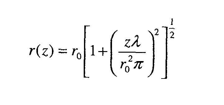
- the increase in the beam size as a function of the free space propagation distance can be calculated according to the Gaussian beam theory.
- the length of free space light path in this system is preferably in the range of from about 600 ⁇ m to about 800 ⁇ m and will introduce a beam divergence problem.
- the first movable mirror 131 can, for example, be made spherically curved to converge the light beam.
- the reflectivity is shown in FIG. 8.
- the wavelength of the light source used in this measurement was 1.55 ⁇ m. Without gold coating, the reflectivity ranges from 32% to 37%, depending on the incident angles of light.
- a polysilicon mirror after chemical mechanical polish has a reflectivity similar to that of a SCS mirror.
- CMP chemical mechanical polish
- a polysilicon mirror module would provide an overall reflectivity close to that of SCS mirrors. After the mirrors are moved to their final positions, the platform supporting these mirrors will be glued to these positions and the voltages on the comb drives will be turned off.
Landscapes
- Physics & Mathematics (AREA)
- General Physics & Mathematics (AREA)
- Optics & Photonics (AREA)
- Optical Couplings Of Light Guides (AREA)
- Mechanical Light Control Or Optical Switches (AREA)
- Micromachines (AREA)
Abstract
Description
Claims (9)
- An integrated alignment mirror module comprising:a substrate (101) having a first surface and a second surface, the substrate having a groove (110) formed in and extending along the first surface and parallel to the second surface;a groove end reflector (113) formed in an end of the groove in the first substrate;a layer having a first region, the layer being attached to the first surface;a first substrate mirror (131) fashioned from the first region of the layer;an optical device (135) on the first wafer; andan optical path extending between the groove (110) and the optical device (131) via optical communication between the groove end reflector (113) and the first substrate mirror (131) whereby light emitted from one of the optical device and an object, such as an optical fibre, in the groove travels to the other of the optical device and the object in the groove via the optical path.
- The module of claim 1, wherein the first substrate mirror (131) is positioned on a platform (139) movable during a calibration of the module, thereby allowing adjustment of the optical path.
- The module of claim 1, comprising a plurality of substrate mirrors in the optical path, at least one of the plurality of substrate mirrors being positioned on a respective platform (139,140) movable during a calibration of the module, thereby allowing further adjustment of the optical path during calibration of the module.
- A module according to claim 2 or claim 3, wherein one or more of the movable mirrors is supported by a respective electrostatic comb drive (139,140) allowing positional adjustment of the mirror.
- A module according to any of the preceding claims, wherein the groove end reflector (113) is inclined at less than 90 degrees as measured from an imaginary extension of the bottom of the groove to a surface of the end.
- A module according to any of the preceding claims, wherein the substrate is a wafer.
- A method comprising:forming a groove (110) in a substrate (101) on which an optical device resides (135);forming a groove end reflector (113) at an end of the groove (110);forming first and second actuators (139,140) on a surface of the substrate;forming first and second substrate mirrors (131,133) on the first and second actuators (139,140), respectively, to establish an optical path between the groove end reflector (113) and the optical device (135);mounting an optical component, such as an optical fiber (10), in the groove with an end of the component in optical communication with the groove end reflector (113) so that light can travel between the optical path and the end of the optical component;causing light to travel along the optical path;adjusting positions of the first and second substrate mirrors (131,133) with their respective actuators (139,140) to maximize light transmission between the optical device and the optical component; andaffixing the first and second substrate mirrors (131,133) in respective positions corresponding to maximized light transmission on the optical path.
- The method of claim 7, wherein forming the actuators (139,140) includes the steps of depositing a layer of material on the substrate, then removing a portion of the material to leave the actuators behind on the surface of the substrate.
- The method of claim 7 or claim 8, wherein forming the substrate mirrors (131,133) includes the steps of depositing a layer of material on at least the actuators (139,140), then removing a portion of the material to leave the substrate mirrors behind on the surface of the respective actuators.
Applications Claiming Priority (2)
| Application Number | Priority Date | Filing Date | Title |
|---|---|---|---|
| US844574 | 1997-04-18 | ||
| US09/844,574 US6580858B2 (en) | 2001-04-30 | 2001-04-30 | Micro-opto-electro-mechanical system (MOEMS) |
Publications (3)
| Publication Number | Publication Date |
|---|---|
| EP1255149A2 true EP1255149A2 (en) | 2002-11-06 |
| EP1255149A3 EP1255149A3 (en) | 2003-09-24 |
| EP1255149B1 EP1255149B1 (en) | 2013-10-16 |
Family
ID=25293103
Family Applications (1)
| Application Number | Title | Priority Date | Filing Date |
|---|---|---|---|
| EP02252944.0A Expired - Lifetime EP1255149B1 (en) | 2001-04-30 | 2002-04-25 | A micro-opto-electro-mechanical system (MOEMS) |
Country Status (3)
| Country | Link |
|---|---|
| US (1) | US6580858B2 (en) |
| EP (1) | EP1255149B1 (en) |
| JP (1) | JP2003014997A (en) |
Cited By (1)
| Publication number | Priority date | Publication date | Assignee | Title |
|---|---|---|---|---|
| CN103827716A (en) * | 2011-09-28 | 2014-05-28 | Fci公司 | Optical system with alignment adjustment |
Families Citing this family (39)
| Publication number | Priority date | Publication date | Assignee | Title |
|---|---|---|---|---|
| US6911392B2 (en) * | 2001-08-24 | 2005-06-28 | Schott Glas | Process for making contact with and housing integrated circuits |
| JP4485790B2 (en) * | 2001-08-24 | 2010-06-23 | ショット アクチエンゲゼルシャフト | Process for manufacturing microelectromechanical components |
| US6782185B2 (en) * | 2002-07-03 | 2004-08-24 | Sumitomo Electric Industries, Ltd. | Optical variable attenuator and optical module |
| US7319260B1 (en) | 2002-10-17 | 2008-01-15 | The United States Of America As Represented By The Secretary Of The Air Force | Hinged bonding of micromechanical devices |
| US7067892B1 (en) | 2002-10-17 | 2006-06-27 | The United States Of America As Represented By The Secretary Of The Air Force | Off substrate flip-chip apparatus |
| US6936493B1 (en) | 2002-10-17 | 2005-08-30 | The United States Of America As Represented By The Secretary Of The Air Force | Micromechanical device latching |
| JP4732711B2 (en) * | 2003-05-23 | 2011-07-27 | アイピー・キューブ・パートナーズ・カンパニー・リミテッド | Etching method for micromachining crystalline material and device manufactured thereby |
| US7136554B1 (en) * | 2003-07-03 | 2006-11-14 | Lockheed Martin Corporation | Post-packaging optical coupling |
| US7410816B2 (en) * | 2004-03-24 | 2008-08-12 | Makarand Gore | Method for forming a chamber in an electronic device and device formed thereby |
| US7162112B2 (en) | 2004-11-23 | 2007-01-09 | Xerox Corporation | Microfabrication process for control of waveguide gap size |
| US7931373B2 (en) * | 2004-12-03 | 2011-04-26 | The Invention Science Fund I, Llc | Vision modification with reflected image |
| US7486988B2 (en) * | 2004-12-03 | 2009-02-03 | Searete Llc | Method and system for adaptive vision modification |
| US8244342B2 (en) * | 2004-12-03 | 2012-08-14 | The Invention Science Fund I, Llc | Method and system for adaptive vision modification |
| US7350919B2 (en) * | 2004-12-03 | 2008-04-01 | Searete Llc | Vision modification with reflected image |
| US8104892B2 (en) * | 2004-12-03 | 2012-01-31 | The Invention Science Fund I, Llc | Vision modification with reflected image |
| US7470027B2 (en) * | 2004-12-03 | 2008-12-30 | Searete Llc | Temporal vision modification |
| US9155483B2 (en) | 2004-12-03 | 2015-10-13 | The Invention Science Fund I, Llc | Vision modification with reflected image |
| US7334894B2 (en) * | 2004-12-03 | 2008-02-26 | Searete, Llc | Temporal vision modification |
| US7594727B2 (en) * | 2004-12-03 | 2009-09-29 | Searete Llc | Vision modification with reflected image |
| US7390088B2 (en) * | 2004-12-03 | 2008-06-24 | Searete Llc | Adjustable lens system with neural-based control |
| US7344244B2 (en) * | 2004-12-03 | 2008-03-18 | Searete, Llc | Adjustable lens system with neural-based control |
| US7334892B2 (en) * | 2004-12-03 | 2008-02-26 | Searete Llc | Method and system for vision enhancement |
| US7656569B2 (en) * | 2004-12-03 | 2010-02-02 | Searete Llc | Vision modification with reflected image |
| US20080112885A1 (en) | 2006-09-06 | 2008-05-15 | Innurvation, Inc. | System and Method for Acoustic Data Transmission |
| EP2231019B1 (en) | 2007-12-10 | 2014-10-22 | Stc.Unm | Photoacoustic imaging devices and methods of imaging |
| US7802928B2 (en) * | 2008-01-04 | 2010-09-28 | Honeywell International Inc. | System and method for fiber based resonator coupling |
| US8529441B2 (en) | 2008-02-12 | 2013-09-10 | Innurvation, Inc. | Ingestible endoscopic optical scanning device |
| US20100016662A1 (en) * | 2008-02-21 | 2010-01-21 | Innurvation, Inc. | Radial Scanner Imaging System |
| US8014682B2 (en) * | 2008-04-18 | 2011-09-06 | Freescale Semiconductor, Inc. | Free-space optical communication system |
| US8260151B2 (en) * | 2008-04-18 | 2012-09-04 | Freescale Semiconductor, Inc. | Optical communication integration |
| WO2010005571A2 (en) | 2008-07-09 | 2010-01-14 | Innurvation, Inc. | Displaying image data from a scanner capsule |
| US8647259B2 (en) | 2010-03-26 | 2014-02-11 | Innurvation, Inc. | Ultrasound scanning capsule endoscope (USCE) |
| US9054024B2 (en) * | 2012-02-13 | 2015-06-09 | Futurewei Technologies, Inc. | Apparatus and method for optical communications |
| JP6200642B2 (en) * | 2012-11-30 | 2017-09-20 | 日本オクラロ株式会社 | Optical device |
| US10349543B2 (en) | 2013-02-22 | 2019-07-09 | Vibrant Composites Inc. | Layered assemblies |
| WO2014130967A2 (en) * | 2013-02-22 | 2014-08-28 | Pratheev Sreetharan | Layered assemblies |
| US10146020B1 (en) * | 2017-05-30 | 2018-12-04 | Google Llc | MEMS steering mirrors for applications in photonic integrated circuits |
| US10281663B1 (en) | 2018-01-08 | 2019-05-07 | Juniper Networks, Inc. | Photonic integrated circuit with active alignment |
| US11487059B2 (en) | 2021-02-19 | 2022-11-01 | Globalfoundries U.S. Inc. | Photonics integrated circuit with silicon nitride waveguide edge coupler |
Family Cites Families (16)
| Publication number | Priority date | Publication date | Assignee | Title |
|---|---|---|---|---|
| US4240695A (en) * | 1979-06-20 | 1980-12-23 | E. I. Du Pont De Nemours And Company | Optical fibers connector |
| US5330926A (en) * | 1990-11-14 | 1994-07-19 | Nec Corporation | Method of fabricating semiconductor device having a trenched cell capacitor |
| JP3484543B2 (en) * | 1993-03-24 | 2004-01-06 | 富士通株式会社 | Method of manufacturing optical coupling member and optical device |
| US5535293A (en) * | 1994-12-09 | 1996-07-09 | Buchin; Michael P. | High-speed electro-optical modulator, chopper, and multiplexer/demultiplexer |
| JP3187286B2 (en) * | 1995-07-10 | 2001-07-11 | 旭光学工業株式会社 | How to adjust the optical axis of an optical pickup |
| US5742419A (en) * | 1995-11-07 | 1998-04-21 | The Board Of Trustees Of The Leland Stanford Junior Universtiy | Miniature scanning confocal microscope |
| US6301403B1 (en) * | 1996-07-30 | 2001-10-09 | Iolon, Inc. | Optical microswitch with rotary electrostatic microactuator |
| US5872880A (en) * | 1996-08-12 | 1999-02-16 | Ronald S. Maynard | Hybrid-optical multi-axis beam steering apparatus |
| US5867297A (en) * | 1997-02-07 | 1999-02-02 | The Regents Of The University Of California | Apparatus and method for optical scanning with an oscillatory microelectromechanical system |
| US6071426A (en) * | 1997-12-08 | 2000-06-06 | The Regents Of The University Of California | Micro benchtop optics by bulk silicon micromachining |
| US6115521A (en) * | 1998-05-07 | 2000-09-05 | Trw Inc. | Fiber/waveguide-mirror-lens alignment device |
| US6320993B1 (en) * | 1998-06-05 | 2001-11-20 | Astarte Fiber Networks, Inc. | Optical switch pathway configuration using control signals |
| US6205274B1 (en) * | 1998-07-20 | 2001-03-20 | Honeywell Inc. | Fiber optic header for an edge emitting laser |
| US6302523B1 (en) * | 1999-07-19 | 2001-10-16 | Xerox Corporation | Ink jet printheads |
| US6363183B1 (en) * | 2000-01-04 | 2002-03-26 | Seungug Koh | Reconfigurable and scalable intergrated optic waveguide add/drop multiplexing element using micro-opto-electro-mechanical systems and methods of fabricating thereof |
| US6356689B1 (en) * | 2000-03-25 | 2002-03-12 | Lucent Technologies, Inc. | Article comprising an optical cavity |
-
2001
- 2001-04-30 US US09/844,574 patent/US6580858B2/en not_active Expired - Fee Related
-
2002
- 2002-04-23 JP JP2002120185A patent/JP2003014997A/en active Pending
- 2002-04-25 EP EP02252944.0A patent/EP1255149B1/en not_active Expired - Lifetime
Cited By (1)
| Publication number | Priority date | Publication date | Assignee | Title |
|---|---|---|---|---|
| CN103827716A (en) * | 2011-09-28 | 2014-05-28 | Fci公司 | Optical system with alignment adjustment |
Also Published As
| Publication number | Publication date |
|---|---|
| US20020168144A1 (en) | 2002-11-14 |
| US6580858B2 (en) | 2003-06-17 |
| JP2003014997A (en) | 2003-01-15 |
| EP1255149B1 (en) | 2013-10-16 |
| EP1255149A3 (en) | 2003-09-24 |
Similar Documents
| Publication | Publication Date | Title |
|---|---|---|
| EP1255149B1 (en) | A micro-opto-electro-mechanical system (MOEMS) | |
| EP3410166B1 (en) | Mems steering mirrors for applications in photonic integrated circuits | |
| EP3803482B1 (en) | Device and method for coupling laser to a photonic integrated circuit | |
| US5577142A (en) | Optical fiber transmitting and receiving communications device | |
| US6115521A (en) | Fiber/waveguide-mirror-lens alignment device | |
| JP5208351B2 (en) | Optical device | |
| US5854867A (en) | Optical module having lenses aligned on lens-positioning V-groove and fabrication method thereof | |
| KR100277695B1 (en) | Method for manufacturing a substrate for hybrid optical integrated circuit using S-O optical waveguide | |
| US6965714B2 (en) | Integrated aspheric optical coupler for RF planarized automatic photonics packaging | |
| US20020096686A1 (en) | Optical interconnect with integral reflective surface and lens, system including the interconnect and method of forming the same | |
| US6985647B2 (en) | Optical module | |
| JPH08204288A (en) | Optical semiconductor device | |
| CN106461882A (en) | Method of forming fiber coupling device and fiber coupling device | |
| US6187515B1 (en) | Optical integrated circuit microbench system | |
| US20120114293A1 (en) | Optical waveguide structure having angled mirror and lens | |
| US20040188788A1 (en) | Optical apparatus using vertical light receiving element | |
| US8090266B2 (en) | Optically coupling components of a transceiver | |
| CN111527431A (en) | temperature insensitive filter | |
| KR19980045943A (en) | Micro-mirror for hybrid optical integrated circuit, manufacturing method thereof, micro mirror-photodetector assembly and hybrid optical integrated circuit assembly for optical reception | |
| JP3795869B2 (en) | Optical module | |
| US9664866B2 (en) | Optical transmission module and manufacturing method thereof | |
| JPH11326662A (en) | Optical planar circuit | |
| JP3468774B2 (en) | Optical coupling device | |
| JPH07191236A (en) | Optical circuit and its production | |
| JP2009192816A (en) | Bidirectional optical transceiver module and light receiving element used therefor |
Legal Events
| Date | Code | Title | Description |
|---|---|---|---|
| PUAI | Public reference made under article 153(3) epc to a published international application that has entered the european phase |
Free format text: ORIGINAL CODE: 0009012 |
|
| AK | Designated contracting states |
Kind code of ref document: A2 Designated state(s): AT BE CH CY DE DK ES FI FR GB GR IE IT LI LU MC NL PT SE TR |
|
| AX | Request for extension of the european patent |
Free format text: AL;LT;LV;MK;RO;SI |
|
| PUAL | Search report despatched |
Free format text: ORIGINAL CODE: 0009013 |
|
| AK | Designated contracting states |
Kind code of ref document: A3 Designated state(s): AT BE CH CY DE DK ES FI FR GB GR IE IT LI LU MC NL PT SE TR |
|
| AX | Request for extension of the european patent |
Extension state: AL LT LV MK RO SI |
|
| RIC1 | Information provided on ipc code assigned before grant |
Ipc: 7G 02B 6/35 B Ipc: 7G 02B 6/42 B Ipc: 7G 02B 26/02 A |
|
| 17P | Request for examination filed |
Effective date: 20040324 |
|
| AKX | Designation fees paid |
Designated state(s): DE FR GB |
|
| 17Q | First examination report despatched |
Effective date: 20040622 |
|
| GRAP | Despatch of communication of intention to grant a patent |
Free format text: ORIGINAL CODE: EPIDOSNIGR1 |
|
| INTG | Intention to grant announced |
Effective date: 20130627 |
|
| GRAS | Grant fee paid |
Free format text: ORIGINAL CODE: EPIDOSNIGR3 |
|
| GRAA | (expected) grant |
Free format text: ORIGINAL CODE: 0009210 |
|
| AK | Designated contracting states |
Kind code of ref document: B1 Designated state(s): DE FR GB |
|
| REG | Reference to a national code |
Ref country code: GB Ref legal event code: FG4D |
|
| REG | Reference to a national code |
Ref country code: DE Ref legal event code: R096 Ref document number: 60245647 Country of ref document: DE Effective date: 20131212 |
|
| REG | Reference to a national code |
Ref country code: DE Ref legal event code: R097 Ref document number: 60245647 Country of ref document: DE |
|
| PLBE | No opposition filed within time limit |
Free format text: ORIGINAL CODE: 0009261 |
|
| STAA | Information on the status of an ep patent application or granted ep patent |
Free format text: STATUS: NO OPPOSITION FILED WITHIN TIME LIMIT |
|
| 26N | No opposition filed |
Effective date: 20140717 |
|
| REG | Reference to a national code |
Ref country code: DE Ref legal event code: R097 Ref document number: 60245647 Country of ref document: DE Effective date: 20140717 |
|
| REG | Reference to a national code |
Ref country code: FR Ref legal event code: PLFP Year of fee payment: 15 |
|
| REG | Reference to a national code |
Ref country code: FR Ref legal event code: PLFP Year of fee payment: 16 |
|
| PGFP | Annual fee paid to national office [announced via postgrant information from national office to epo] |
Ref country code: FR Payment date: 20170322 Year of fee payment: 16 |
|
| PGFP | Annual fee paid to national office [announced via postgrant information from national office to epo] |
Ref country code: GB Payment date: 20170324 Year of fee payment: 16 |
|
| PGFP | Annual fee paid to national office [announced via postgrant information from national office to epo] |
Ref country code: DE Payment date: 20170321 Year of fee payment: 16 |
|
| REG | Reference to a national code |
Ref country code: DE Ref legal event code: R119 Ref document number: 60245647 Country of ref document: DE |
|
| GBPC | Gb: european patent ceased through non-payment of renewal fee |
Effective date: 20180425 |
|
| PG25 | Lapsed in a contracting state [announced via postgrant information from national office to epo] |
Ref country code: DE Free format text: LAPSE BECAUSE OF NON-PAYMENT OF DUE FEES Effective date: 20181101 |
|
| PG25 | Lapsed in a contracting state [announced via postgrant information from national office to epo] |
Ref country code: GB Free format text: LAPSE BECAUSE OF NON-PAYMENT OF DUE FEES Effective date: 20180425 |
|
| PG25 | Lapsed in a contracting state [announced via postgrant information from national office to epo] |
Ref country code: FR Free format text: LAPSE BECAUSE OF NON-PAYMENT OF DUE FEES Effective date: 20180430 |