EP1253729A2 - Reducing scintillation effects for optical free-space transmission - Google Patents
Reducing scintillation effects for optical free-space transmission Download PDFInfo
- Publication number
- EP1253729A2 EP1253729A2 EP02252093A EP02252093A EP1253729A2 EP 1253729 A2 EP1253729 A2 EP 1253729A2 EP 02252093 A EP02252093 A EP 02252093A EP 02252093 A EP02252093 A EP 02252093A EP 1253729 A2 EP1253729 A2 EP 1253729A2
- Authority
- EP
- European Patent Office
- Prior art keywords
- sdram
- page
- read
- submatrix
- write
- Prior art date
- Legal status (The legal status is an assumption and is not a legal conclusion. Google has not performed a legal analysis and makes no representation as to the accuracy of the status listed.)
- Granted
Links
Images





Classifications
-
- H—ELECTRICITY
- H04—ELECTRIC COMMUNICATION TECHNIQUE
- H04L—TRANSMISSION OF DIGITAL INFORMATION, e.g. TELEGRAPHIC COMMUNICATION
- H04L1/00—Arrangements for detecting or preventing errors in the information received
- H04L1/004—Arrangements for detecting or preventing errors in the information received by using forward error control
- H04L1/0056—Systems characterized by the type of code used
- H04L1/0057—Block codes
-
- H—ELECTRICITY
- H03—ELECTRONIC CIRCUITRY
- H03M—CODING; DECODING; CODE CONVERSION IN GENERAL
- H03M13/00—Coding, decoding or code conversion, for error detection or error correction; Coding theory basic assumptions; Coding bounds; Error probability evaluation methods; Channel models; Simulation or testing of codes
- H03M13/03—Error detection or forward error correction by redundancy in data representation, i.e. code words containing more digits than the source words
- H03M13/05—Error detection or forward error correction by redundancy in data representation, i.e. code words containing more digits than the source words using block codes, i.e. a predetermined number of check bits joined to a predetermined number of information bits
- H03M13/13—Linear codes
- H03M13/15—Cyclic codes, i.e. cyclic shifts of codewords produce other codewords, e.g. codes defined by a generator polynomial, Bose-Chaudhuri-Hocquenghem [BCH] codes
-
- H—ELECTRICITY
- H03—ELECTRONIC CIRCUITRY
- H03M—CODING; DECODING; CODE CONVERSION IN GENERAL
- H03M13/00—Coding, decoding or code conversion, for error detection or error correction; Coding theory basic assumptions; Coding bounds; Error probability evaluation methods; Channel models; Simulation or testing of codes
- H03M13/27—Coding, decoding or code conversion, for error detection or error correction; Coding theory basic assumptions; Coding bounds; Error probability evaluation methods; Channel models; Simulation or testing of codes using interleaving techniques
-
- H—ELECTRICITY
- H04—ELECTRIC COMMUNICATION TECHNIQUE
- H04B—TRANSMISSION
- H04B10/00—Transmission systems employing electromagnetic waves other than radio-waves, e.g. infrared, visible or ultraviolet light, or employing corpuscular radiation, e.g. quantum communication
- H04B10/11—Arrangements specific to free-space transmission, i.e. transmission through air or vacuum
-
- H—ELECTRICITY
- H04—ELECTRIC COMMUNICATION TECHNIQUE
- H04L—TRANSMISSION OF DIGITAL INFORMATION, e.g. TELEGRAPHIC COMMUNICATION
- H04L1/00—Arrangements for detecting or preventing errors in the information received
- H04L1/004—Arrangements for detecting or preventing errors in the information received by using forward error control
- H04L1/0056—Systems characterized by the type of code used
- H04L1/0071—Use of interleaving
Definitions
- Optical free-space transmission is subject to degradation arising from the effects of scintillation in the transmission medium.
- Free-space optical signals experience fading from scintillation over times on the order of several milliseconds. During these times, a multi-gigabit/second signal may lose tens of millions of bits. For example, an 8 millisecond fade in a 2.5 gigabit/second data stream equates to the loss of 20,000,000 bits.
- FEC block-oriented forward error correction
- the degradation arising from scintillation effects in free-space optical transmission can last for millions of bits compared to the typically far shorter duration of error bursts in optical fiber media.
- the single-block FEC error correction process therefore is extremely impractical in correcting errors of the lengths that occur in free-space optical transmission. Addressing the problem resulting from scintillation effects by selective re-transmission of affected blocks is also not practical for such large error bursts, due to the real-time nature of communication processes such as video.
- Interleaving is therefore a candidate for error-correction of scintillation effects in optical free-space transmission, since in theory it can correct for error bursts that last for tens of millions of consecutive bits.
- the communication terminal requires an extraordinarily large encoder/decoder and buffer store under current terminal design concepts. Considerations of cost, size, and power consumed by the scintillation effect error-correction apparatus must be constrained in realizing a commercially practical communication terminal.
- SDRAM Synchronous-dynamic-random-access-memory
- a large number of cycles (7 for example) are required to change page addresses.
- the result of straightforward addressing then is a seven-fold reduction of the effective memory speed.
- the high bit rates involved in optical communications already mandate using the fastest SDRAM devices available to perform this interleaving process. Therefore, such a slowdown would impair the practicality of using SDRAM devices to implement a process of overcoming scintillation effects in optical free-space transmission.
- This invention provides a process and apparatus for encoding-interleaving and deinterleaving-decoding an optical data stream which overcomes transmission degradation from scintillation effects.
- a burst error of the magnitude of 20 million consecutive bits can be masked at an affordable cost in components and a negligible cost in added latency.
- the invention in one embodiment uses SDRAM devices for permutation buffers.
- the invention overcomes the limitations of the typical SDRAM device when used to provide large array permutations, by using an address remapping that essentially equalizes the READ vs. WRITE rates.
- unique advantage is taken of a characteristic of state-of -the-art SDRAM devices, that one can READ or WRITE the devices at the device cycle rate within a page (i.e. row).
- address re-mapping is applied when the number of columns that can be stored in one page is too small - that is, when the overhead cycles of the SDRAM devices amortized over the number of memory references that can occur (as a row is read) before a page change, leads to an effective memory cycle rate that does not meet system requirements.
- Address remapping in accordance with the invention redistributes overhead operations from WRITE to READ, which permits essentially realtime operation with a minimum of elastic memory.
- a physical SDRAM page change occurs - for example -every 15 entries instead of every 512 entries.
- the result is that the overhead associated with row-address changes is made roughly equal in both the WRITE (i.e. input to the permutation buffer) and READ (readout of the permutation buffer). In this way the overhead cycles are amortized over a large number of memory references for both the READ and WRITE process, such that the effective memory cycle rate asymptotically approaches the burst physical cycle rate.
- the invention thus solves the problem of economically managing the very large interleaving or permutation span required to cover error bursts in optical free-space communications of the order of 20 million bits, which would result, for example, if an 8 millisecond fade occurred during a 2.5 gigabit/sec. transmission.
- the invention is described in an illustrative embodiment involving optical free-space communications, the invention also has applicability to, for example, RF wireless communications systems (e.g. millimeter wave). As such systems operate at higher and higher data rates, the fades they experience also create lost megabits. Using the methods and apparatus hereinafter taught, the megabits lost in fades in RF wireless communications may be recovered.
- RF wireless communications systems e.g. millimeter wave
- Fig. 1 is a schematic block diagram of an optical free-space communication system
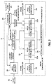
- Fig, 2 is a schematic block diagram illustrating a transmitter-end system and components to perform the invention
- Fig. 3 is a diagram illustrating segmenting of codewords to prepare for interleaving
- Fig. 4 is a flow chart showing a protocol for interleaving blocks of codeword segments
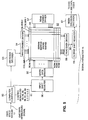
- Fig. 5 is a schematic block diagram illustrating a receiver-end system and components to perform the invention
- Fig. 6A is a diagram illustrating remapping of addresses in SDRAM matrix to balance "READ” vs. "WRITE" overhead in terms of SDRAM page changes;
- Fig. 6B is a diagram illustrating another exemplary way to remap SDRAM addresses to balance "READ” vs. "WRITE" overhead;
- Fig. 6C is a diagram illustrating consequences of holding a received matrix on one 512-address page if receiver stores entries sequentially;
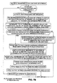
- Fig. 7A is a flow chart of the process including address remapping at the transmit end.
- Fig. 7B is a flow chart of the process including address remapping at the receive end.
- the principle of interleaving moderately sized burst-error correction code blocks is used, but on a macro scale much larger than conventionally applied, such that the interleaving for the examples illustrated spans hundreds of millions of bits in order to support recovery from burst errors on the order of tens of millions of bits.
- Synchronous Dynamic Random Access Memory (SDRAM) device technology is used by way of example, to make it feasible and economical to support the extremely large memory arrays that are required to implement such a process.
- SDRAM Synchronous Dynamic Random Access Memory
- the effect of the address remapping is that overhead cycle bursts are distributed rather than occurring in clusters of consecutive memory references, which is typical when a straightforward use of memory address space is applied. This allows the invention's high-speed memory reference rate to be maintained with minimal elasticity in the data flow.
- the effects of scintillation degradation in free-space optical transmission can vary as a function of many ambient conditions. For example, for a point-to-point optical range of 4.4 km. and a crosswind on the order of 10 mph, the temporal correlation of scintillation is on the order of 15 milliseconds. For a range of 1km. and 10 mph. crosswind, the time scale is 7-8 milliseconds. If the crosswind is on the order of 20 mph. in the range of 1km., the temporal correlation becomes about 4 milliseconds.
- the extent of scintillation effect also varies as a function of other atmospheric conditions including, for example, air temperature, emissions and relative humidity. The onset of scintillation conditions can also be determined by the monitoring of the received signal of the reverse path of a free space optical link.
- the invention is illustrated as part of an optical free-space transmission system seen in FIG. 1.
- the system receives at an input end a data stream payload 10.
- the payload may be in the form of a continuous data stream; or may comprise data bursts where the bit-length of the payload may vary from burst to burst.
- the burst-error correction process may be applied unconditionally and continuously to all data transmitted; or may be selectively applied when certain free-space conditions such as just described are detected, for example, by sensors 19. Sensors 19 are linked to computer controller 26, where instructions contain threshold values which determine whether the free-space scintillation conditions are present. If the free-space medium conditions are occurring, data stream payload 10 is routed through signal conditioner 11. Here, the data is encoded and interleaved into a buffer store in a manner to be described. The output of signal conditioner 11 is transmitted by transmitter 12, for transmission through free-space medium 13 to a receiver 14. If the received signal has been conditioned for scintillation, it is fed to signal extractor 15 for de-interleaving and decoding before being routed for end use in, for example, video or high-speed data applications.
- signal conditioner 11 comprises encoder 20 which preferably is of the (255,223) Reed-Solomon type.
- a data stream payload 10 of 2.5 gbit is fed to Reed-Solomon encoder 20, which outputs a 2.86 gbit stream in this illustrative embodiment.
- Reed-Solomon coding is used having a Galois Field of 8-bit symbols and a (255,223) code configuration.
- Reed-Solomon coding is comprehensively described in the afore-mentioned text "Error Correcting Codes"s, Peterson and Weldon, 1992.
- Encoder 20 encodes the payload data stream 10 into codewords, each of length n as seen in Fig. 3.
- An exemplary codeword 30 is split into the desired number (for example, 30) of codeword fragments, of which for convenience only six fragments 30a-30f are shown.
- the next codeword then is similarly fragmented into 34 fragments; and these latter fragments are interleaved with the previous thirty-four fragments.
- the interleaving of codewords occurs over a span sufficiently large that the burst error of length E bits will affect at most b bits in any given codeword.
- Methodologies for effecting the interleaving are well-known, one example being described in US 5,889,791 which is hereby incorporated by reference.
- Fig. 4 shows a sequence of steps by which segments of each codeword may be denoted by a 2-tuple where n is the codeword number and m is a 60-bit segment within the denoted codeword.
- the first block of 156,250 codewords are interleaved into cells of buffer 22.
- the codeword sequence is shown by the bracketed number sequences, which reveal the writing of "column entries" for subsequent READOUT as rows.
- an erasure or loss of any two of the bracketed sequences incurs no more than 120 bits of error in any codeword.
- a 60-bit input shift register 21 receives the encoder 20 output.
- Sixty-bit segments of the codeword are chosen because 60 is an integer factor of 2040 and 60 bits x 156,250 x 2 is close to the nominal 20 megabit burst-error length objective of 18.75 megabits.
- a burst error of 18.75 million bits would destroy two 60-bit segments (120 bits) in each of 156,250 interleaved codewords, but because all of the codewords have the capability of correcting 128 bits, all the data would be recovered in the example.
- Input shift register 21 distributes the fragments created in encoder 20 to a buffer store 22 comprising a bank of eight SDRAMs 22a....22h, ganged in groups of four.
- the SDRAMs are 16 bit X 8 megaword stores.
- the SDRAM devices are loaded in accordance with addresses supplied by Field Programmable Gate Array (FPGA) configured as address generators 23, 24.
- FPGA Field Programmable Gate Array
- the operation of buffer store 22, and FPGA address generators 23, 24 are directed by computer controller 26.
- READOUT from the SDRAM devices is to output shift register 25, which feeds transmitter 12 with a stream of encoded and interleaved bits.
- a substantially identical buffer store 52 at the receiver is used to deinterleave; and is described hereinafter and in Fig. 5.
- the encoding processes of encoder 20, the addressing functions of address generators 23, 24 the storage functions of SDRAMs 22a..h, and the operation of input and output shift registers 21,25 may be performed in separate hardware components with functionalities coordinated by instruction code run in computer controller 26 shown in Fig. 2. If hardware is preferred, suitable commercially available components are: Vitesse Semiconductor VSC 7146 device for the shift registers 21, 25; and Lucent Technology's ORCA FPGA ORT8850 components for the address generators 23, 24.
- the functions of address generators 23, 24 and input shift registers 21,25, as well as encoder 20, may alternatively be provided as code instructions under the control of computer controller 26.
- the Reed-Solomon code uses a Galios Field of 8-bit symbols and a (255-233) code.
- a codeword is 255 octets (bytes) in length, of which 223 are payload, with the remaining 32 as check symbols.
- the code has the capability of correcting 32/2 or 16 bytes of error. This means that as few as 16 isolated errors (i.e. if each error were in a different octet) could be corrected; but that as many as 16 x 8 or 128 bit errors would be corrected in any block if the errors all occurred within 16 bytes.
- a buffer store of this size may be realized by using SDRAMs of 128 or 256 megabits in size.
- the WRITE process to SDRAM devices in buffer store 22 requires forming 60-bit words in 20.8 ns. (60 times the bit period of the 2.8 x 10 9 bit/sec. encoded data stream).
- Performing interleaving in a straightforward manner involves writing entries at address increments of 156,250 (i. e., matrix column entries), then READING out consecutive addresses (rows) to transmit the interleaved codewords.
- Parameters peculiar to state-of-the-art SDRAM devices make this difficult, because of latency effects vis-à-vis isolated READ or WRITE operations.
- Micron Technologies SDRAM device no. MT48LC8M16A2 This is exemplified by the characteristics of the Micron Technologies SDRAM device no. MT48LC8M16A2. More information on this and similar SDRAM devices from Micron Technologies Inc. may be obtained at their WebSite at http://www.micron.com. Other manufacturers also produce SDRAM devices; and it is understood that all such similar devices may be adapted by persons skilled in the art to practice the invention.
- Class-2 SDRAM In order to realize performance with the minimum of overhead operations in the SDRAM devices, it is desirable to use Class-2 SDRAM with a maximum clock rate of 133 MHz., or 7.5 ns. cycle time. However, this seven cycle WRITE epoch associated with the SDRAM devices of buffer store 22 is not compatible with 20.8 ns. READOUT rate at which new 60-bit codeword segments are being generated.
- the invention takes unique advantage of a characteristic of the state-of -the-art SDRAM devices, which is that one can READ or WRITE to the devices at the device cycle rate within a page (i.e. row).
- consecutively-addressed READ operands can asymptotically be performed at a 7.5 ns. rate, which is well under the 20.7 ns. rate required for real-time transmissions.
- the general remapping strategy therefore is to equalizing "READ” vs. "WRITE” rates.
- the idea is to regard each page in SDRAM memory as multiple "virtual" pages; and exploit the fast WRITE rate on the same (physical) page in exchange for requiring a more frequent page change during READ in the permutation operation.
- the general approach is to WRITE K consecutive entries into one physical page, with the result that the READ process must then change pages [K] times as often compared with simply READING each P-entry page of SDRAM as a single sequence of consecutive addresses (where P is the page size).
- each physical 512-word SDRAM page is defined as consisting of 34 pages of 15 words each (two words are wasted). Since the permutation matrix is 34x150250 in size, the number 34 is selected to make indexing systematic.
- the signal extractor 15 at the receiver includes a computer controller 50 and an SDRAM buffer store 52 which may be substantially identical in construction to buffer store 22 at the transmitter.
- the buffer store is depicted as a matrix of memory cells such as cell 51, each cell being defined by the intersections of rows 1, 2, ..., R and columns 1, 2, ..., C.
- Computer controller 50 receives the encoded and interleaved signal 9 transmitted from transmitter 12 through free-space medium 13.
- An address decoder 53 controlled by computer controller 50 acquires the address information associated with each received interleaved codeword segment such as segment 30f in Fig. 3, and specifies the cell addresses in buffer store 52 into which the sequentially-received codeword segments are to be stored.
- Each row of cells of buffer store 52 is served by a WRITE enable driver 54; and each column of cells of buffer store 52 is served by a WRITE data driver 55.
- Addresses to which to send the interleaved segments are supplied by address decoder 53 to WRITE enable driver 54.
- the received interleaved codeword segments are assembled in input shift register 56 and forwarded to WRITE data driver 55.
- WRITE data driver 55 transfers segments to the memory cell matrix of SDRAM buffer store 52.
- a READ enable driver 57 is connected to each row of memory cells. of SDRAM buffer store 52, and a READ data driver 58 is connected to each column of cells of SDRAM buffer store 52.
- READout from SDRAM buffer store 52 is preceded by determining in computer controller 50 whether the matrix of SDRAM buffer store 52, if mapped in the straightforward manner, will not slow down the process when read; or whether instead the need exists to remap the matrix to execute the deinterleaving in such a way as to equalize READ VS. WRITE rates.
- the READout data from Buffer store 22 is accumulated in output shift register 59; and the deinterleaved output data stream 60 is thereafter directed to Reed-Solomon decoder 61 which decodes the deinterleaved data stream.
- a deinterleaved and decoded data stream 62 is channeled from Reed-Solomon decoder 61 to an end use in video or data applications.
- Control signal paths all denoted 51 for simplicity, are provided from computer controller 50 to the functions 53, 54, 55, 56, 57, 58 and 59.
- buffer store 52 is read by activating READ enable driver 57 to read data from the matrix accessed by READ data driver 58.
- Remapping of physical addresses where needed is performed in accordance with the following criteria. In general, whether at the transmitter or the receiver, address remapping is performed when the number of matrix columns that can be stored in one page of SDRAM buffer store 52 is too small - which is the case when the overhead cycles amortized over the number of memory references that can occur (as a row is read) before a page change, leads to an effective memory cycle rate that does not meet system requirements. For the particular device speed parameters used in the herein example, the number of columns that must be held on one page must be 4 or greater.
- a first-in, first-out elastic memory of 4 entries provides a means to bridge the page change.
- the 52.5 ns. interruption incurred by the page change is effectively masked with a backlog of 3 entries in the elastic memory.
- Figs. 6A, 6B and 6C The remapping of addresses in the matrix of buffer store 52 is illustrated in Figs. 6A, 6B and 6C.
- Remapping addresses in the matrix of buffer store 22 is accomplished in the same fashion as hereinafter. described).
- entries 1,1 1,2 ....1,34 are stored in physical addresses 0,15, Vietnamese, 495 of the first SDRAM page. However, these are treated during the READ operation as addresses 0, 156,250, Vietnamese,33x156,250 respectively. Because the factorization of addresses maps has the row length as one factor, exactly 15 rows of 34 entries in this example fit into one physical page.
- the "virtual" addresses illustrated in Fig. 6A refer to the sequence in which the READout is performed to complete the permutation.
- the same matrix is received by row into the matrix of SDRAM buffer store 52.
- This matrix must be transposed effect a de-interleaving. If the received entries were written sequentially into SDRAM buffer store 52 as depicted in Fig. 6C, the result would be a page change every 512 memory references during WRITE, but the subsequent READ by column of the matrix would require SDRAM page changes every memory reference. This would mean that real-time operation could not be maintained with the example parameters.
- Exact equalization of READ and WRITE overhead advantageously involves choosing a square submatrix with dimensions equal to the square root of the page size. For the example parameters (512-word page size) this is not integer. Any submatrix dimensioning (where the submatrix represents the set of entries to be written on a single physical page) is satisfactory for which the minimum matrix dimension (representing the number of successive memory references that occur before a page change) is sufficient to amortize the SDRAM overhead for a page change. This amortization is dependent on the relationship of the maximum burst rate of the memory versus the transfer rate of new entries to be read or written The excess of burst rate versus transfer rate must be sufficient to cover the overhead cycles. Thus, for the example with a 20.8 ns. entry receive or transmit rate, a 7.5 ns SDRAM rate on one page, and a 52.5 ns SDRAM page-change overhead, amortizing the overhead over 15 memory references is more than sufficient to maintain real time with an elastic store of 4 words.
- the parameters of the above example require choosing a large data fragment, or word size, (60 bits) due to the high speed of the data stream and the need to thereby reduce the system clock rate to a value compatible with readily available memory and digital logic devices.
- word size 60 bits
- the number of such words involved in decomposing the Reed-Solomon codeword of 2040 bits for purposes of interleaving is only 34. This does not provide a sufficient number of consecutive memory references between page changes to amortize the 7 cycle overhead, when the input words are stored in consecutive addresses; and hence address remapping is applied.
- Fig. 7A summarizes the key process steps described above, which provide a balance of SDRAM READ vs. WRITE operations at the transmit end.
- Fig. 7B illustrates the key process steps of deinterleaving at the receive end a coded and interleaved signal generated by the process and apparatus at the transmit end.
Landscapes
- Engineering & Computer Science (AREA)
- Physics & Mathematics (AREA)
- Computer Networks & Wireless Communication (AREA)
- Signal Processing (AREA)
- Theoretical Computer Science (AREA)
- Probability & Statistics with Applications (AREA)
- General Physics & Mathematics (AREA)
- Algebra (AREA)
- Electromagnetism (AREA)
- Mathematical Physics (AREA)
- Pure & Applied Mathematics (AREA)
- Error Detection And Correction (AREA)
- Detection And Prevention Of Errors In Transmission (AREA)
- Detection And Correction Of Errors (AREA)
- Memory System (AREA)
- Time-Division Multiplex Systems (AREA)
- Optical Communication System (AREA)
- Road Signs Or Road Markings (AREA)
Abstract
Description
The process involves first conventionally encoding the data stream into codewords or blocks each of n bits comprising k payload bits and (n-k) error-correcting-code-bits. The process then defines the maximum number of errors that can be corrected within a codeword as b, taking into account that the maximum number of bits that can be corrected by any linear code is:
1,1 1,2 1,3 .....1,34
and in general the n'th entry in codeword m is denoted m, n.
Claims (10)
- A process for transmitting a transmission payload data bit-stream through a free-space medium, said process comprising the steps of:encoding a transmission payload data bit-stream into codewords;fragmenting each said codeword into segments;in a SDRAM buffer store having an entry receive and transmit rate and comprising a matrix of memory cells, defining an x-y submatrix of said cells representing the set of entries comprising a single SDRAM physical page;in a WRITE operation having a first page-change overhead operation, interleaving corresponding segments of successive said codewords into said submatrix of cells;in a READ operation having a second page-change overhead operation, reading out the contents of said submatrix of cells: andtransmitting the encoded and interleaved data-bit stream of said READ operation into said medium;said WRITE and READ operations into and out of said submatrix of cells being conducted to substantially redistribute page change overhead operations from said WRITE operation to said READ operation, thereby to equalize the rate of said WRITE and READ operations.
- The process of claim 1, wherein the step of encoding of said transmission payload data bit-stream into codewords is effected using Reed-Solomon coding.
- The process of claim 2, further comprising the step of dimensioning said submatrix of cells such that the minimum matrix dimension representing the number of successive memory references that occur before a page change during a said READ operation is sufficient to amortize SDRAM overhead for a said page change.
- The process of claim 3, wherein said redistribution of page change overhead operations from said WRITE operation to said READ operation comprises the further steps of:WRITING into successive columns of said submatrix cells corresponding segments of successive said codewords comprising a said SDRAM page; andremapping submatrix cell addresses for READout to maintain the number of columns held on one page to a number that ensures a physical SDRAM page change at intervals which makes the READ and WRITE rates substantially equal.
- The process of claim 4, comprising the further steps of:sensing conditions in said medium which cause scintillation effects; andactivating said encoding and interleaving steps when said conditions are detected.
- The process of claims 1, 2, 3, 4 or 5, further comprising the step of:at a remote receiver, deinterleaving said corresponding segments of successive said codewords to reproduce said encoded data-bit stream; anddecoding said encoded data-bit stream.
- Apparatus for transmitting a transmission payload data bit-stream through an optical free-space medium, said apparatus comprising:means for encoding an optical transmission payload data bit-stream into codewords using Reed-Solomon encoding;means for fragmenting each said codeword into segments;a SDRAM buffer store having an entry receive and transmit rate and comprising a matrix of memory cells,said SDRAM buffer store further having a defined repeating x-y submatrix of said cells representing the set of entries comprising a single SDRAM physical page;means for effecting a WRITE operation to interleave corresponding segments of successive said codewords into said repeating submatrix of cells:said WRITE operation having an associated first page-change overhead operation,means for effecting in a READ operation to read out the contents of said submatrix of cells;said READ operation having an associated second page-change overhead operation,said WRITE and READ operations into and out of said submatrix of cells being conducted to substantially redistribute page change overhead operations from said WRITE operation to said READ operation, thereby to equalize the rate of said WRITE and READ operations; andmeans for transmitting the encoded and interleaved data-bit stream of said READ operation into said medium.
- Apparatus in accordance with claim 7, further comprising:means for dimensioning said submatrix of cells such that the minimum matrix dimension representing the number of successive memory references that occur before a page change during a said READ operation is sufficient to amortize SDRAM overhead for a said page change.
- Apparatus in accordance with claim 8, wherein said redistribution of page change overhead operations from said WRITE operation to said READ operation further comprises:apparatus for WRITING into successive columns of said submatrix cells corresponding segments of successive said codewords comprising a said SDRAM page; andapparatus for remapping submatrix cell addresses for READout to maintain the number of columns held on one page to a number that ensures a physical SDRAM page change at intervals which makes the READ and WRITE rates substantially equal.
- Apparatus in accordance with claims 7, 8 or 9, wherein:said SDRAM buffer store comprises a storage cell capacity sufficiently large to correct an error burst of the order of 20 million bits;said Reed-Solomon code is of the (255,223) format;said encoding means encodes said incoming data stream into substantially 156,250 codewords to be interleaved;said codeword size is 2040 bits; andsaid segmenting means segments each said codeword into 60-bit segments for interleaving in said submatrices of said SDRAM buffer store.
Applications Claiming Priority (2)
| Application Number | Priority Date | Filing Date | Title |
|---|---|---|---|
| US09/839,486 US6868519B2 (en) | 2001-04-23 | 2001-04-23 | Reducing scintillation effects for optical free-space transmission |
| US839486 | 2001-04-23 |
Publications (3)
| Publication Number | Publication Date |
|---|---|
| EP1253729A2 true EP1253729A2 (en) | 2002-10-30 |
| EP1253729A3 EP1253729A3 (en) | 2004-07-28 |
| EP1253729B1 EP1253729B1 (en) | 2005-07-13 |
Family
ID=25279853
Family Applications (1)
| Application Number | Title | Priority Date | Filing Date |
|---|---|---|---|
| EP02252093A Expired - Lifetime EP1253729B1 (en) | 2001-04-23 | 2002-03-22 | Reducing scintillation effects for optical free-space transmission |
Country Status (5)
| Country | Link |
|---|---|
| US (1) | US6868519B2 (en) |
| EP (1) | EP1253729B1 (en) |
| JP (1) | JP4108359B2 (en) |
| AT (1) | ATE299627T1 (en) |
| DE (1) | DE60204994T2 (en) |
Cited By (9)
| Publication number | Priority date | Publication date | Assignee | Title |
|---|---|---|---|---|
| EP1478117A3 (en) * | 2003-05-12 | 2005-01-05 | Lucent Technologies Inc. | Method of real time hybrid ARQ |
| GB2497154A (en) * | 2012-08-30 | 2013-06-05 | Imagination Tech Ltd | Tile-based interleaving or de-interleaving using a burst-mode DRAM |
| EP3697007A1 (en) * | 2019-02-15 | 2020-08-19 | INTEL Corporation | Low-latency forward error correction for high-speed serial links |
| US11153032B2 (en) | 2017-02-28 | 2021-10-19 | Intel Corporation | Forward error correction mechanism for peripheral component interconnect-express (PCI-E) |
| US11223446B2 (en) | 2018-12-18 | 2022-01-11 | Intel Corporation | Forward error correction mechanism for data transmission across multi-lane links |
| US11249837B2 (en) | 2019-03-01 | 2022-02-15 | Intel Corporation | Flit-based parallel-forward error correction and parity |
| US11296994B2 (en) | 2019-05-13 | 2022-04-05 | Intel Corporation | Ordered sets for high-speed interconnects |
| US11740958B2 (en) | 2019-11-27 | 2023-08-29 | Intel Corporation | Multi-protocol support on common physical layer |
| US12189470B2 (en) | 2020-09-18 | 2025-01-07 | Intel Corporation | Forward error correction and cyclic redundancy check mechanisms for latency-critical coherency and memory interconnects |
Families Citing this family (19)
| Publication number | Priority date | Publication date | Assignee | Title |
|---|---|---|---|---|
| DK1245027T3 (en) * | 1999-12-17 | 2004-11-15 | Thomson Licensing Sa | Use of an SDRAM as storage for correction and trace intermediate storage in front end IDs for optical recording or reproducing devices |
| US7158517B2 (en) * | 2001-05-21 | 2007-01-02 | Intel Corporation | Method and apparatus for frame-based protocol processing |
| JP4077355B2 (en) * | 2003-04-16 | 2008-04-16 | 三菱電機株式会社 | Communication apparatus and communication method |
| US8644341B1 (en) * | 2003-09-26 | 2014-02-04 | Sigma Designs Israel S.D.I. Ltd | MAC structure with packet-quasi-static blocks and ARQ |
| KR100596435B1 (en) | 2003-12-17 | 2006-07-05 | 주식회사 하이닉스반도체 | Semiconductor memory device can reduce address access time |
| US7835264B2 (en) * | 2004-12-29 | 2010-11-16 | Mitsubishi Denki Kabushiki Kaisha | Interleaver, deinterleaver, communication device, and method for interleaving and deinterleaving |
| US20060176966A1 (en) * | 2005-02-07 | 2006-08-10 | Stewart Kenneth A | Variable cyclic prefix in mixed-mode wireless communication systems |
| US20060245384A1 (en) * | 2005-05-02 | 2006-11-02 | Talukdar Anup K | Method and apparatus for transmitting data |
| US7649788B2 (en) * | 2006-01-30 | 2010-01-19 | Unity Semiconductor Corporation | Buffering systems for accessing multiple layers of memory in integrated circuits |
| KR100764052B1 (en) * | 2006-08-03 | 2007-10-08 | 삼성전자주식회사 | Flash memory device having a floating address boundary and its program method |
| US8400998B2 (en) * | 2006-08-23 | 2013-03-19 | Motorola Mobility Llc | Downlink control channel signaling in wireless communication systems |
| WO2009031134A2 (en) * | 2007-09-04 | 2009-03-12 | Hayim Shaul | Apparatus and method for representing a sequence of content as projections and for reconstructing the sequence at full or lower quality |
| US7941711B2 (en) * | 2007-12-04 | 2011-05-10 | Texas Instruments Incorporated | Determining bit error rate using single data burst |
| CN102801488B (en) * | 2011-05-23 | 2015-12-16 | 中兴通讯股份有限公司 | A kind ofly be applicable to the intertexture of WiMAX or the implementation method of deinterleaving and device |
| FR2986889B1 (en) * | 2012-02-09 | 2014-10-17 | Thales Sa | PAYMENT SYSTEM, PAYMENT TERMINAL OF THE SYSTEM, AND PAYMENT METHOD THEREOF |
| JP6988092B2 (en) * | 2017-01-16 | 2022-01-05 | 富士通株式会社 | Parallel processing device and burst error reproduction method |
| US10289330B2 (en) * | 2017-03-30 | 2019-05-14 | Western Digital Technologies, Inc. | Allocating shared memory among multiple tasks in a multiprocessor environment |
| CN109495207B (en) * | 2017-09-11 | 2021-08-10 | 上海诺基亚贝尔股份有限公司 | Method and apparatus for interleaving data in wireless communication system |
| US20250112697A1 (en) * | 2023-09-28 | 2025-04-03 | Rosemount Aerospace Inc. | Aircraft to airport laser communication |
Family Cites Families (10)
| Publication number | Priority date | Publication date | Assignee | Title |
|---|---|---|---|---|
| US5063533A (en) * | 1989-04-10 | 1991-11-05 | Motorola, Inc. | Reconfigurable deinterleaver/interleaver for block oriented data |
| US5907563A (en) * | 1996-03-07 | 1999-05-25 | Kokusai Denshin Denwa Co. Ltd. | Error control method and apparatus for wireless data communication |
| US5889791A (en) * | 1996-08-13 | 1999-03-30 | Motorola, Inc. | System, device and method of FEC coding and interleaving for variable length burst transmission |
| US6044429A (en) * | 1997-07-10 | 2000-03-28 | Micron Technology, Inc. | Method and apparatus for collision-free data transfers in a memory device with selectable data or address paths |
| US6075824A (en) * | 1997-08-04 | 2000-06-13 | Motorola, Inc. | Method and apparatus for re-encoding decoded data |
| GB2334641A (en) * | 1998-02-11 | 1999-08-25 | Northern Telecom Ltd | Multiplexed transmission of optical signals |
| JP4110613B2 (en) * | 1998-04-22 | 2008-07-02 | ソニー株式会社 | Transmitting apparatus, transmitting method, providing medium, and transmission system |
| US6163871A (en) * | 1998-05-29 | 2000-12-19 | Adaptec, Inc. | RAM based error correction code encoder and syndrome generator with programmable interleaving degrees |
| DE19951677B4 (en) * | 1998-10-30 | 2006-04-13 | Fujitsu Ltd., Kawasaki | Semiconductor memory device |
| US6625763B1 (en) * | 2000-07-05 | 2003-09-23 | 3G.Com, Inc. | Block interleaver and de-interleaver with buffer to reduce power consumption |
-
2001
- 2001-04-23 US US09/839,486 patent/US6868519B2/en not_active Expired - Lifetime
-
2002
- 2002-03-22 EP EP02252093A patent/EP1253729B1/en not_active Expired - Lifetime
- 2002-03-22 DE DE60204994T patent/DE60204994T2/en not_active Expired - Lifetime
- 2002-03-22 AT AT02252093T patent/ATE299627T1/en not_active IP Right Cessation
- 2002-04-22 JP JP2002119003A patent/JP4108359B2/en not_active Expired - Fee Related
Cited By (16)
| Publication number | Priority date | Publication date | Assignee | Title |
|---|---|---|---|---|
| US7408913B2 (en) | 2003-05-12 | 2008-08-05 | Lucent Technologies Inc. | Method of real time hybrid ARQ |
| EP1478117A3 (en) * | 2003-05-12 | 2005-01-05 | Lucent Technologies Inc. | Method of real time hybrid ARQ |
| GB2497154A (en) * | 2012-08-30 | 2013-06-05 | Imagination Tech Ltd | Tile-based interleaving or de-interleaving using a burst-mode DRAM |
| GB2497154B (en) * | 2012-08-30 | 2013-10-16 | Imagination Tech Ltd | Tile based interleaving and de-interleaving for digital signal processing |
| US11153032B2 (en) | 2017-02-28 | 2021-10-19 | Intel Corporation | Forward error correction mechanism for peripheral component interconnect-express (PCI-E) |
| US11223446B2 (en) | 2018-12-18 | 2022-01-11 | Intel Corporation | Forward error correction mechanism for data transmission across multi-lane links |
| US11637657B2 (en) | 2019-02-15 | 2023-04-25 | Intel Corporation | Low-latency forward error correction for high-speed serial links |
| EP3697007A1 (en) * | 2019-02-15 | 2020-08-19 | INTEL Corporation | Low-latency forward error correction for high-speed serial links |
| US12355565B2 (en) | 2019-02-15 | 2025-07-08 | Intel Corporation | Low-latency forward error correction for high-speed serial links |
| US11934261B2 (en) | 2019-03-01 | 2024-03-19 | Intel Corporation | Flit-based parallel-forward error correction and parity |
| US11249837B2 (en) | 2019-03-01 | 2022-02-15 | Intel Corporation | Flit-based parallel-forward error correction and parity |
| US11595318B2 (en) | 2019-05-13 | 2023-02-28 | Intel Corporation | Ordered sets for high-speed interconnects |
| US11296994B2 (en) | 2019-05-13 | 2022-04-05 | Intel Corporation | Ordered sets for high-speed interconnects |
| US11740958B2 (en) | 2019-11-27 | 2023-08-29 | Intel Corporation | Multi-protocol support on common physical layer |
| US12242336B2 (en) | 2019-11-27 | 2025-03-04 | Intel Corporation | Multi-protocol support on common physical layer |
| US12189470B2 (en) | 2020-09-18 | 2025-01-07 | Intel Corporation | Forward error correction and cyclic redundancy check mechanisms for latency-critical coherency and memory interconnects |
Also Published As
| Publication number | Publication date |
|---|---|
| US20020157060A1 (en) | 2002-10-24 |
| ATE299627T1 (en) | 2005-07-15 |
| DE60204994T2 (en) | 2006-04-27 |
| EP1253729A3 (en) | 2004-07-28 |
| JP2003051813A (en) | 2003-02-21 |
| EP1253729B1 (en) | 2005-07-13 |
| DE60204994D1 (en) | 2005-08-18 |
| JP4108359B2 (en) | 2008-06-25 |
| US6868519B2 (en) | 2005-03-15 |
Similar Documents
| Publication | Publication Date | Title |
|---|---|---|
| US6868519B2 (en) | Reducing scintillation effects for optical free-space transmission | |
| EP0681373B1 (en) | Convolutional interleaver with reduced memory requirements and address generator therefor | |
| JP3996205B2 (en) | Concatenated code data transmission / reception method and transmission / reception apparatus | |
| US5983388A (en) | Forward error correction arrangement (FEC) for multipoint to single point communication systems | |
| US8453037B2 (en) | Turbo coding having combined turbo de-padding and rate matching de-padding | |
| CN1350369A (en) | Storage device, method for accessing storage device and Read-solomon decoder | |
| WO2002013449A2 (en) | Apparatus and method for providing turbo code interleaving in a communications system | |
| CN100488057C (en) | Optimized interleaving of digital signals | |
| US20080092009A1 (en) | Error Correction Coding Apparatus and Error Correction Decoding Apparatus | |
| KR100699491B1 (en) | Interleaving method and apparatus | |
| JP2008135813A (en) | Turbo decoder and turbo decoding method | |
| US6329935B1 (en) | Temporally separating and re-organizing data using two-stage interleaving and de-interleaving | |
| US7886203B2 (en) | Method and apparatus for bit interleaving and deinterleaving in wireless communication systems | |
| KR100499467B1 (en) | Block interleaving method, and apparatus for the same | |
| US10819469B2 (en) | High speed interleaver/deinterleaver device supporting line rate, and method thereof | |
| JPH03242027A (en) | Parallel error correction system with interleaving function added | |
| US7103820B2 (en) | System and method for interleaving forward error correction code words across multiple communication connections | |
| JP2003101419A (en) | Interleaved transmitter and receiver | |
| KR100733767B1 (en) | Time deinterleaving apparatus and method | |
| US20040267968A1 (en) | Implementation of a column interleaving function with a limited amount of columns | |
| Chi | Helical interleavers | |
| HK1101296A1 (en) | Transmitter and receiver for transmitting digital information packets using forward error correction | |
| HK1101296B (en) | Transmitter and receiver for transmitting digital information packets using forward error correction |
Legal Events
| Date | Code | Title | Description |
|---|---|---|---|
| PUAI | Public reference made under article 153(3) epc to a published international application that has entered the european phase |
Free format text: ORIGINAL CODE: 0009012 |
|
| 17P | Request for examination filed |
Effective date: 20020412 |
|
| AK | Designated contracting states |
Kind code of ref document: A2 Designated state(s): AT BE CH CY DE DK ES FI FR GB GR IE IT LI LU MC NL PT SE TR |
|
| AX | Request for extension of the european patent |
Free format text: AL;LT;LV;MK;RO;SI |
|
| PUAL | Search report despatched |
Free format text: ORIGINAL CODE: 0009013 |
|
| AK | Designated contracting states |
Kind code of ref document: A3 Designated state(s): AT BE CH CY DE DK ES FI FR GB GR IE IT LI LU MC NL PT SE TR |
|
| AX | Request for extension of the european patent |
Extension state: AL LT LV MK RO SI |
|
| 17Q | First examination report despatched |
Effective date: 20040827 |
|
| GRAP | Despatch of communication of intention to grant a patent |
Free format text: ORIGINAL CODE: EPIDOSNIGR1 |
|
| AKX | Designation fees paid |
Designated state(s): AT BE CH CY DE DK ES FI FR GB GR IE IT LI LU MC NL PT SE TR |
|
| GRAS | Grant fee paid |
Free format text: ORIGINAL CODE: EPIDOSNIGR3 |
|
| GRAA | (expected) grant |
Free format text: ORIGINAL CODE: 0009210 |
|
| AK | Designated contracting states |
Kind code of ref document: B1 Designated state(s): AT BE CH CY DE DK ES FI FR GB GR IE IT LI LU MC NL PT SE TR |
|
| PG25 | Lapsed in a contracting state [announced via postgrant information from national office to epo] |
Ref country code: IT Free format text: LAPSE BECAUSE OF FAILURE TO SUBMIT A TRANSLATION OF THE DESCRIPTION OR TO PAY THE FEE WITHIN THE PRESCRIBED TIME-LIMIT;WARNING: LAPSES OF ITALIAN PATENTS WITH EFFECTIVE DATE BEFORE 2007 MAY HAVE OCCURRED AT ANY TIME BEFORE 2007. THE CORRECT EFFECTIVE DATE MAY BE DIFFERENT FROM THE ONE RECORDED. Effective date: 20050713 Ref country code: BE Free format text: LAPSE BECAUSE OF FAILURE TO SUBMIT A TRANSLATION OF THE DESCRIPTION OR TO PAY THE FEE WITHIN THE PRESCRIBED TIME-LIMIT Effective date: 20050713 Ref country code: CH Free format text: LAPSE BECAUSE OF FAILURE TO SUBMIT A TRANSLATION OF THE DESCRIPTION OR TO PAY THE FEE WITHIN THE PRESCRIBED TIME-LIMIT Effective date: 20050713 Ref country code: AT Free format text: LAPSE BECAUSE OF FAILURE TO SUBMIT A TRANSLATION OF THE DESCRIPTION OR TO PAY THE FEE WITHIN THE PRESCRIBED TIME-LIMIT Effective date: 20050713 Ref country code: FI Free format text: LAPSE BECAUSE OF FAILURE TO SUBMIT A TRANSLATION OF THE DESCRIPTION OR TO PAY THE FEE WITHIN THE PRESCRIBED TIME-LIMIT Effective date: 20050713 Ref country code: LI Free format text: LAPSE BECAUSE OF FAILURE TO SUBMIT A TRANSLATION OF THE DESCRIPTION OR TO PAY THE FEE WITHIN THE PRESCRIBED TIME-LIMIT Effective date: 20050713 Ref country code: NL Free format text: LAPSE BECAUSE OF FAILURE TO SUBMIT A TRANSLATION OF THE DESCRIPTION OR TO PAY THE FEE WITHIN THE PRESCRIBED TIME-LIMIT Effective date: 20050713 Ref country code: TR Free format text: LAPSE BECAUSE OF FAILURE TO SUBMIT A TRANSLATION OF THE DESCRIPTION OR TO PAY THE FEE WITHIN THE PRESCRIBED TIME-LIMIT Effective date: 20050713 |
|
| REG | Reference to a national code |
Ref country code: GB Ref legal event code: FG4D |
|
| REG | Reference to a national code |
Ref country code: CH Ref legal event code: EP |
|
| REG | Reference to a national code |
Ref country code: IE Ref legal event code: FG4D |
|
| REF | Corresponds to: |
Ref document number: 60204994 Country of ref document: DE Date of ref document: 20050818 Kind code of ref document: P |
|
| PG25 | Lapsed in a contracting state [announced via postgrant information from national office to epo] |
Ref country code: GR Free format text: LAPSE BECAUSE OF FAILURE TO SUBMIT A TRANSLATION OF THE DESCRIPTION OR TO PAY THE FEE WITHIN THE PRESCRIBED TIME-LIMIT Effective date: 20051013 Ref country code: SE Free format text: LAPSE BECAUSE OF FAILURE TO SUBMIT A TRANSLATION OF THE DESCRIPTION OR TO PAY THE FEE WITHIN THE PRESCRIBED TIME-LIMIT Effective date: 20051013 Ref country code: DK Free format text: LAPSE BECAUSE OF FAILURE TO SUBMIT A TRANSLATION OF THE DESCRIPTION OR TO PAY THE FEE WITHIN THE PRESCRIBED TIME-LIMIT Effective date: 20051013 |
|
| PG25 | Lapsed in a contracting state [announced via postgrant information from national office to epo] |
Ref country code: ES Free format text: LAPSE BECAUSE OF FAILURE TO SUBMIT A TRANSLATION OF THE DESCRIPTION OR TO PAY THE FEE WITHIN THE PRESCRIBED TIME-LIMIT Effective date: 20051024 |
|
| PG25 | Lapsed in a contracting state [announced via postgrant information from national office to epo] |
Ref country code: PT Free format text: LAPSE BECAUSE OF FAILURE TO SUBMIT A TRANSLATION OF THE DESCRIPTION OR TO PAY THE FEE WITHIN THE PRESCRIBED TIME-LIMIT Effective date: 20051219 |
|
| NLV1 | Nl: lapsed or annulled due to failure to fulfill the requirements of art. 29p and 29m of the patents act | ||
| REG | Reference to a national code |
Ref country code: CH Ref legal event code: PL |
|
| PG25 | Lapsed in a contracting state [announced via postgrant information from national office to epo] |
Ref country code: IE Free format text: LAPSE BECAUSE OF NON-PAYMENT OF DUE FEES Effective date: 20060322 |
|
| PG25 | Lapsed in a contracting state [announced via postgrant information from national office to epo] |
Ref country code: MC Free format text: LAPSE BECAUSE OF NON-PAYMENT OF DUE FEES Effective date: 20060331 Ref country code: LU Free format text: LAPSE BECAUSE OF NON-PAYMENT OF DUE FEES Effective date: 20060331 |
|
| ET | Fr: translation filed | ||
| PLBE | No opposition filed within time limit |
Free format text: ORIGINAL CODE: 0009261 |
|
| STAA | Information on the status of an ep patent application or granted ep patent |
Free format text: STATUS: NO OPPOSITION FILED WITHIN TIME LIMIT |
|
| 26N | No opposition filed |
Effective date: 20060418 |
|
| REG | Reference to a national code |
Ref country code: IE Ref legal event code: MM4A |
|
| PG25 | Lapsed in a contracting state [announced via postgrant information from national office to epo] |
Ref country code: CY Free format text: LAPSE BECAUSE OF FAILURE TO SUBMIT A TRANSLATION OF THE DESCRIPTION OR TO PAY THE FEE WITHIN THE PRESCRIBED TIME-LIMIT Effective date: 20050713 |
|
| REG | Reference to a national code |
Ref country code: GB Ref legal event code: 732E Free format text: REGISTERED BETWEEN 20131031 AND 20131106 |
|
| REG | Reference to a national code |
Ref country code: FR Ref legal event code: CD Owner name: ALCATEL-LUCENT USA INC. Effective date: 20131122 |
|
| REG | Reference to a national code |
Ref country code: FR Ref legal event code: GC Effective date: 20140410 |
|
| REG | Reference to a national code |
Ref country code: FR Ref legal event code: RG Effective date: 20141015 |
|
| REG | Reference to a national code |
Ref country code: FR Ref legal event code: PLFP Year of fee payment: 14 |
|
| PGFP | Annual fee paid to national office [announced via postgrant information from national office to epo] |
Ref country code: DE Payment date: 20150327 Year of fee payment: 14 |
|
| PGFP | Annual fee paid to national office [announced via postgrant information from national office to epo] |
Ref country code: FR Payment date: 20150317 Year of fee payment: 14 Ref country code: GB Payment date: 20150327 Year of fee payment: 14 |
|
| REG | Reference to a national code |
Ref country code: DE Ref legal event code: R119 Ref document number: 60204994 Country of ref document: DE |
|
| GBPC | Gb: european patent ceased through non-payment of renewal fee |
Effective date: 20160322 |
|
| REG | Reference to a national code |
Ref country code: FR Ref legal event code: ST Effective date: 20161130 |
|
| PG25 | Lapsed in a contracting state [announced via postgrant information from national office to epo] |
Ref country code: FR Free format text: LAPSE BECAUSE OF NON-PAYMENT OF DUE FEES Effective date: 20160331 Ref country code: GB Free format text: LAPSE BECAUSE OF NON-PAYMENT OF DUE FEES Effective date: 20160322 Ref country code: DE Free format text: LAPSE BECAUSE OF NON-PAYMENT OF DUE FEES Effective date: 20161001 |