EP1253641A2 - Semiconductor device provided with fuse and method of disconnecting fuse - Google Patents
Semiconductor device provided with fuse and method of disconnecting fuse Download PDFInfo
- Publication number
- EP1253641A2 EP1253641A2 EP02252413A EP02252413A EP1253641A2 EP 1253641 A2 EP1253641 A2 EP 1253641A2 EP 02252413 A EP02252413 A EP 02252413A EP 02252413 A EP02252413 A EP 02252413A EP 1253641 A2 EP1253641 A2 EP 1253641A2
- Authority
- EP
- European Patent Office
- Prior art keywords
- fuse
- insulating film
- semiconductor device
- wiring
- protective member
- Prior art date
- Legal status (The legal status is an assumption and is not a legal conclusion. Google has not performed a legal analysis and makes no representation as to the accuracy of the status listed.)
- Withdrawn
Links
Images





Classifications
-
- H—ELECTRICITY
- H10—SEMICONDUCTOR DEVICES; ELECTRIC SOLID-STATE DEVICES NOT OTHERWISE PROVIDED FOR
- H10D—INORGANIC ELECTRIC SEMICONDUCTOR DEVICES
- H10D84/00—Integrated devices formed in or on semiconductor substrates that comprise only semiconducting layers, e.g. on Si wafers or on GaAs-on-Si wafers
- H10D84/01—Manufacture or treatment
-
- H—ELECTRICITY
- H10—SEMICONDUCTOR DEVICES; ELECTRIC SOLID-STATE DEVICES NOT OTHERWISE PROVIDED FOR
- H10W—GENERIC PACKAGES, INTERCONNECTIONS, CONNECTORS OR OTHER CONSTRUCTIONAL DETAILS OF DEVICES COVERED BY CLASS H10
- H10W20/00—Interconnections in chips, wafers or substrates
- H10W20/40—Interconnections external to wafers or substrates, e.g. back-end-of-line [BEOL] metallisations or vias connecting to gate electrodes
- H10W20/49—Adaptable interconnections, e.g. fuses or antifuses
- H10W20/493—Fuses, i.e. interconnections changeable from conductive to non-conductive
- H10W20/494—Fuses, i.e. interconnections changeable from conductive to non-conductive changeable by the use of an external beam, e.g. laser beam or ion beam
Definitions
- the present invention relates to a semiconductor device provided with a fuse to be disconnected by a laser and to a method of disconnecting a fuse provided on a semiconductor circuit.
- a redundant circuit is sometimes provided inside a semiconductor device.
- the semiconductor device provided with such a redundant circuit is generally designed to use a fuse in order to switch a defective circuit to the redundant circuit.
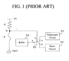
- Fig. 1 is a view showing one example of a method of switching circuits with a fuse.
- a redundant circuit 51 has a constitution identical to that of a basic circuit 52. This redundant circuit 51 is connected with a contact point a of a switch circuit 53 and the basic circuit 52 is connected with a contact point b of the switch circuit 53. A center tap c of the switch circuit 53 is connected with a buffer 54. Moreover, a control terminal s of the switch circuit 53 is connected with a node N between a resistor R and a fuse F. The resistor R and the fuse F are serially connected between a power source line Vh and a ground line Vgnd.
- the electric potential of the control terminal s of the switch circuit 53 is equal to the electric potential of the ground line Vgnd (which is referred to as a "L" level), and the center tap c of the switch circuit 53 is connected with the contact point b. Therefore, the buffer 54 is electrically connected with the basic circuit 52 and electrically separated from the redundant circuit 51.
- the fuse F is disconnected by a laser. Accordingly, the electric potential of the control terminal s of the switch circuit 53 is made equal to the electric potential of the power source line Vh (which is referred to as a "H" level), whereby the center tap c and the contact point a are connected. Therefore, the buffer 54 is electrically connected with the redundant circuit 51 and electrically separated from the basic circuit 52.
- the defective circuit can be switched into the redundant circuit by disconnecting the fuse F by a laser.
- Fig. 2 is a cross-sectional view showing a conventional semiconductor device provided with a fuse.
- An insulating film 62 is formed on a semiconductor substrate 61, and lower wiring including lines 63a and 63b is formed on this insulating film 62.
- Another insulating film 64 is formed on both of the insulating film 62 and the lower wiring, and a fuse 65 is formed on the insulating film 64. Both ends of this fuse 65 are electrically connected with the lower lines 63a and 63b severally through via contact portions 64a and 64b formed inside the insulating film 64.
- Another insulating film 66 is formed on both of the insulating film 64 and the fuse 65.
- a laser is irradiated onto the center portion of the fuse 65 via the insulating film 66 when the fuse 65 is disconnected.
- the center portion of the fuse 65 irradiated by the laser is heated up above the melting point thereof and changed from a solid phase to a liquid phase or a gas phase, and a sudden rise of pressure causes a so-called thermal explosion.
- the fuse 65 is disconnected by this thermal explosion, and a part of the insulating film 66 (an upper part of the disconnected portion of the fuse) is exfoliated as shown in Fig. 3.
- the thermal explosion occurs upon disconnecting the fuse 65 by the laser.
- large pressure is also applied to the insulating film 64 under the fuse 65, whereby a part of the insulating films 64 and 62 may be exfoliated and a crack may also occur in the insulating film 64 and 62.
- damages such as exfoliation or cracks occur in the insulating films 64 and 62, water may easily infiltrate into the semiconductor substrate 61 and a wiring layer, thus causing deterioration of characteristics.
- Japanese Patent Laid-Open No. Hei 9 (1997)-36234 discloses a fuse, which is composed of first and second fuse elements disposed vertically via an insulating film, and a contact portion which connects tip portions of these first and second fuse elements electrically.
- Japanese Patent Laid-Open No. Hei 9 (1997)-36234 also discloses a fuse, in which the first and the second fuse elements are formed in the same layer, whereby the fuse is composed by electrically connecting the first and the second fuse elements with the contact portion. These fuses are designed as surely disconnectable by irradiating a laser onto the contact portion.
- Japanese Patent Laid-Open No. Hei 4 (1992)-14245 discloses a fuse composed of a partially thinned aluminum line, in which a member easily heated by a laser (a heating member) such as a polysilicon film is disposed under the fuse. According to the publication, the fuse made of aluminum can be surely disconnected by means of heating the heating member by the laser to cause thermal explosion.
- a semiconductor device includes a semiconductor substrate, an insulating film formed on the semiconductor substrate, a fuse formed on the insulating film, and a protective member formed stronger than the insulating film and disposed under a disconnecting point of the fuse.
- the high-strength protective member is disposed under the disconnecting point of the fuse.
- the temperature at the disconnecting point is suddenly increased and thermal explosion occurs.
- the protective member protects the lower insulating film, whereby occurrence of damages such as exfoliation and cracks can be prevented.
- the thermal explosion occurs on the high-strength protective member, destructive pressure is concentrated on an upper side of the protective member. In this way, the fuse can be efficiently disconnected. In addition, a form of destruction of the fuse is also stabilized.
- Only one protective member may be disposed per fuse, or a plurality of protective members may be also disposed. Moreover, in the case of a semiconductor device provided with a plurality of fuses, it is preferable that the fuses are arrayed within a certain area in consideration of operating efficiency upon disconnection of the fuses.
- a method of disconnecting a fuse is a method of disconnecting a fuse of a semiconductor device including a semiconductor substrate, a first insulating film formed on the semiconductor substrate, wiring formed on the first insulating film, a second insulating film formed on the first insulating film and the wiring, a fuse formed on the second insulating film, and a via contact portion formed inside the second insulating film to connect the fuse and the wiring electrically, in which the fuse is disconnected by irradiating a laser onto a connective portion of the fuse to the via contact portion.
- the via contact portion is also used as the protective member, whereby the fuse is disconnected by irradiating the laser onto the connective portion of the fuse to the via contact portion.
- the via contact portion protects the insulating film under the fuse, whereby occurrence of damages such as exfoliation and cracks can be prevented.
- another method of disconnecting a fuse is a method of disconnecting a fuse of a semiconductor device including a semiconductor substrate, a first insulating film formed on the semiconductor substrate, wiring formed on the first insulating film, a second insulating film formed on the first insulating film and the wiring, a fuse formed on the second insulating film, a via contact portion formed inside the second insulating film to connect the fuse and the wiring electrically, and a plurality of protective members formed stronger than the second insulating film and disposed separately from one another under the fuse, in which the fuse is disconnected by severally irradiating a laser onto at least one of portions directly above the protective member out of a plurality of the protective numbers.
- the plurality of protective members are provided under the fuse. Then, upon disconnection of the fuse, the laser is irradiated onto upper portions of these protective members. In other words, the fuse is disconnected at a plurality of portions. In this way, the fuse can be surely disconnected. Moreover, upon irradiation of the laser, each of the protective members protects the insulating film under the fuse, whereby occurrence of damages such as exfoliation and cracks can be prevented.
- the fuse may be also disconnected by irradiating the laser onto a portion between the protective members.
- the insulating film under the fuse is also protected by the respective protective members, whereby occurrence of damages such as exfoliation and cracks can be prevented.
- Fig. 4 is a block diagram showing a first embodiment of the present invention applied to a semiconductor memory device.
- one set of memory cell unit consists of sixteen memory cells A0 to A15. Moreover, in the semiconductor memory device, provided for each memory cell unit are one redundant memory cell Ax, sixteen switch circuits S0 to S15, sixteen buffers B0 to B15, one resistor R and sixteen fuses F0 to F15. Such a set of memory cell unit stores 16 bits of data.
- Either one-out of the redundant memory cell Ax or the memory cell A0 is connected with the buffer B0 by a switch circuit S0. Meanwhile, either one out of the memory cell A0 or the memory cell A1 is connected with the buffer B1 by the switch circuit S1. Likewise, either one out of the memory cell An-1 (provided that n is an arbitrary integer in a range from 1 to 15) or the memory cell An is connected with the butter Bn by the switch circuit Sn.
- Each of the switch circuits S0 to S15 is composed of one inverter INV and two switching elements M1 and M2.
- both of the switching elements M1 and M2 are composed of metal-oxide semiconductor (MOS) transistors.
- MOS metal-oxide semiconductor
- the resistor R and the fuses F0 to F15 are serially connected between a power source line (+Vh) and a ground line (Vgnd).
- a control terminal of the switch circuit S0 that is, a node of the input terminal of the inverter INV and the gate of the switching element M1 is connected with a node (N0) between the resister R and the fuse F0.
- the switching element M1 inside the switch circuit S0 When electric potential of the node N0 is at the "L” level, the switching element M1 inside the switch circuit S0 is turned off and the switching element M2 is turned on, whereby the redundant memory cell Ax is electrically separated from the buffer B0 and the memory cell A0 is connected with the buffer B0. Moreover, when the electric potential of the node N0 is at the "H” level, the switching element M1 inside the switch circuit S0 is turned on and the switching element M2 is turned off, whereby the redundant memory cell Ax is electrically connected with the buffer B0 and the memory cell A0 is electrically separated from the buffer B0.
- the buffer Bn and the memory cell An are electrically connected when the electric potential of the node Nn between the fuse Fn-1 and the fuse Fn is at the "L" level, and the buffer Bn and the memory cell An-1 are electrically connected when the electric potential of the node Nn is at the "H" level.
- the switch circuits S0 to S15 When there is no defect among the memory cells A0 to A15, none of the fuses F0 to F15 is disconnected; therefore, the electric potential of the nodes N0 to N15 is at the "L" level, respectively. Accordingly, in the switch circuits S0 to S15, the switching elements M1 are turned off and the switching elements M2 are turned on. As a consequence, the buffer B0 is electrically connected with the memory cell A0, the buffer B1 is electrically connected with the memory cell A1, and the buffer Bn is electrically connected with the memory cell An.
- the fuse F3 will be disconnected by a laser. In this way, the electric potential of the nodes N0 to N3 is changed to the "H" level; meanwhile, the electric potential of the nodes N4 to N15 remains at the "L” level.
- the switching elements M1 are turned on and the switching elements M2 are turned off.
- the buffer B0 is connected with the redundant memory cell Ax
- the buffer B1 is connected with the memory cell A0
- the buffer B2 is connected with the memory cell A1
- the buffer B3 is connected with the memory cell A2.
- the buffer B4 is connected with the memory cell A4; and likewise, the buffer Bm (m is an arbitrary integer in a range from 4 to 15) is connected with the memory cell Am. In this way, the memory cell unit can retain 16-bit data without using the defective memory cell A3.
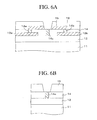
- Figs. 5A and 5B are cross-sectional views showing a structure of a fuse-forming portion of the semiconductor device of this embodiment.
- Fig. 5A shows a cross section in the longitudinal direction of the fuse and
- Fig. 5B shows a cross section in the width direction of the fuse.
- Transistors, resistors (none of those are illustrated) and the like are formed on a semiconductor substrate 11 in order to constitute the circuit as shown in Fig. 4.
- an insulating film 12 made of silicon oxide, for example, is formed on the semiconductor substrate 11, and lower wiring including lines 13a and 13b is formed on the insulating film 12.
- the lower wiring is made of aluminum or an aluminum alloy (hereinafter simply referred to as "the aluminum"), or other metallic materials.
- the insulating film 12 may be also made of phospho-silicate glass (PSG), fluoro-silicate glass (FSG) or other materials.
- An insulating film 14 made of silicon oxide is formed on both of the insulating film 12 and the lower wiring. Moreover, a fuse 15 is formed on the insulating film 14.
- the fuse 15 is made of aluminum.
- the material for the fuse 15 is not limited to aluminum.
- the fuse 15 may be also made of polysilicon, copper or other materials.
- Both end portions of the fuse 15 are electrically connected with the lines 13a and 13b through via contact portions 14a and 14b formed in the insulating film 14, respectively.
- a protective member 14c is disposed under a disconnecting point of the fuse 15 (a portion to irradiate a laser: the central portion of the fuse in this example).
- These via contact portions 14a, 14b and the protective member 14c are formed by burying tungsten (W) into holes after forming the holes in predetermined portions of the insulating film 14.
- the material for the protective member 14c is not limited to tungsten. However, it is essential that the protective member 14c possesses higher strength in comparison with the insulating films in the periphery thereof. Also, it is essential that the material for the protective member 14c possesses higher melting point than the material for the fuse 15. Moreover, although it is preferable from a viewpoint of fabrication that the protective member 14c is made of the same material as that of the via contact portions 14a and 14b, the protective member 14c may be also made of another material different from that of the via contact portions 14a and 14b. For example, the via contact portions 14a and 14b may be made of tungsten; meanwhile, the protective member 14c may be made of copper (Cu).
- An insulating film 16 made of silicon oxide is formed on both of the insulating film 14 and the fuse 15.
- all the insulating films 12, 14 and 16 are made of silicon oxide in this embodiment. However, any of the insulating films 12, 14 and 16 may be made of another insulative material.
- a laser is irradiated onto the central portion of the fuse 15 via the insulating film 16 upon disconnecting the fuse 15.
- the central portion of the fuse 15 is heated up above the melting point thereof, thus causing thermal explosion.
- the fuse 15 is disconnected and the insulating film 16 thereon is partially exfoliated.
- the protective member 14c since thermal explosion occurs above the high-strength protective member 14c, destructive pressure is concentrated on an upper side of the protective member 14c. In this way, the fuse 15 can be efficiently disconnected and a form of destruction of the fuse 15 is also stabilized. In addition, whereas redundant energy after disconnecting the fuse may reach the semiconductor substrate 11 and impart thermal damages thereto, the protective member 14c according to this embodiment reflects or absorbs laser beams, whereby the thermal damages to the semiconductor substrate 11 can be reduced.
- Fig. 7A is a top plan view showing an example of a semiconductor device arraying a plurality of fuses provided with the protective members being disposed thereunder as described above
- Fig. 7B is a top plan view showing the same in the state that the fuses of the semiconductor device are disconnected.
- Figs. 7A and 7B portions identical to those in Figs. 5A and 5B or in Fig. 6A and 6B are denoted by identical reference numerals.
- Figs. 7A and 7B it is preferable to dispose the fuses 15 together in a predetermined region on the semiconductor substrate. In this way, an operation of disconnecting the fuses 15 can be efficiently carried out.
- the insulating film 12 is formed on the whole upper side of the semiconductor substrate 11 by depositing silicon oxide in accordance with a chemical vapor deposition (CVD) method. Thereafter, holes are formed in predetermined positions of the insulating film 12 by use of photolithography. Then, a conductive material such as tungsten is buried into the holes, thus forming via contact portions (not shown) which are electrically connected with the elements.
- CVD chemical vapor deposition
- the aluminum film is patterned by photolithography to form the lower wiring including the lines 13a and 13b.
- the insulating film 14 is formed by depositing silicon oxide on both of the insulating film 12 and the lower wiring by the CVD method. Thereafter, holes are formed in predetermined positions of the insulating film 14 by use of photolithography and then tungsten (W) is buried into the holes, whereby the via contact portions 14a and 14b and the protective member 14c are formed. Then, a surface of the insulating film 14 is subjected to planarization as necessary by chemical mechanical polishing (CMP).
- CMP chemical mechanical polishing
- the insulating film 16 is formed by depositing silicon oxide on both of the insulating film 14 and the fuse 15 in accordance with the CVD method. Thereafter, the insulating film 16 above the disconnecting point of the fuse 15 is etched as necessary to thin the film thickness in the relevant portion.
- the semiconductor device of this embodiment is finished.
- the protective member 14c is formed simultaneously with formation of the via contact portions 14a and 14b. Therefore, it is possible to fabricate the semiconductor device provided with the protective member 14c under the fuse 15 without adding a fabricating step.
- a protective insulating film 17 with Si 3 N 4 or the like depending on a device type in order to avoid infiltration of water into a wiring layer or element portions.
- the protective insulating film 17 is formed between the insulating film 12 and the insulating film 14.
- the holes are formed by etching the insulating film 14 under a condition to raise an etching rate for the insulating film (SiO 2 ) 14 higher than that for the protective insulating film (Si 3 N 4 ) 17, whereby depths of the holes can be controlled.
- the bottom end of the protective member 14c is placed below the protective insulating film 17 as shown in Fig. 10.
- a stopper (a metallic film) 13c made of an aluminum film may be also formed under the protective member 14c in the same step to form the lines 13a and 13b. In this way, the stopper 13c can be prevented from etching to the insulating film 12 upon formation of the hole for the protective member 14c.
- Fig. 12 is a view showing a modified example of the first embodiment.
- Fig. 12 it should be noted that portions identical to those illustrated in Fig. 5A are denoted by identical reference numerals, and detailed description thereto will be omitted.
- a fuse provided on a semiconductor device
- a plurality of the protective members are provided in response to a plurality of disconnecting points.
- protective members 14d and 14e are formed under the disconnecting points (at two points in the drawing) of the fuse 15. These protective members 14d and 14e are formed as similarly to via contact portions 14a and 14b, by forming holes in the insulating film 14 and then burying tungsten (W) into the holes.
- Fig. 13A is a top plan view showing an example of a semiconductor device arraying a plurality of fuses provided with a plurality of protective members thereunder as described above
- Fig. 13B is a top plan view of the same in the state that the fuses of the semiconductor device are disconnected.
- Figs. 13A and 13B portions identical to those in Fig. 12 are denoted by identical reference numerals.
- an operation to disconnect the fuses 15 can be efficiently carried out by disposing the fuses 15 together in a predetermined region on the semiconductor substrate.
- Fig. 14 is a cross-sectional view showing a method of disconnecting a fuse of a semiconductor device according to a second embodiment of the present invention.
- Fig. 14 portions identical to those in Fig. 5A are denoted by identical reference numerals, and detailed description thereto will be omitted.
- a via contact portion 14a connecting a fuse 15 with a lower line 13a is also used as a protective member.
- an end of the fuse which is a node of the via contact portion 14a and the fuse 15 is defined as a disconnecting point.
- tungsten is buried into the via contact potion 14a.
- a laser is irradiated onto the end of the fuse 15 upon disconnection of the fuse 15.
- the end of the fuse 15 is heated up above the melting point thereof, thus causing thermal explosion.
- the via contact portion 14a of this embodiment is made of high-strength tungsten, an insulating film 14 is protected from pressure owing to the thermal explosion.
- redundant energy upon disconnecting the fuse is reflected or absorbed by the via contact portion 14a, thermal damages to a semiconductor substrate 11 are reduced.
- the via contact portion 14a concentrates the pressure upon the thermal explosion toward an upper side of the via contact portion 14a, the fuse 15 can be efficiently disconnected and a form of destruction of the fuse 15 is also stabilized.
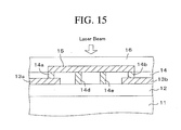
- Fig. 15 is a cross-sectional view showing a method of disconnecting a fuse of a semiconductor device according to a third embodiment of the present invention.
- portions identical to those in Fig. 5A are denoted by identical reference numerals, and detailed description thereto will be omitted.
- protective members 14d and 14e are formed in two positions in the vicinity of a disconnecting point of a fuse 15 (the central portion of the fuse) so that the protective members 14d and 14e sandwich the disconnecting point.
- These protective members 14d and 14e are formed as similarly to via contact portions 14a and 14b, by forming holes in an insulating film 14 and then burying tungsten (W) into the holes.
- a laser is irradiated between the protective members 14d and 14e upon disconnection of the fuse 15.
- the protective members 14d and 14e are buried into the insulating film 14, pressure attributable to thermal explosion upon disconnection of the fuse is relaxed by the protective members 14d and 14e. In this way, damages to the insulating film 14 can be suppressed.
- Fig. 16 is a cross-sectional view showing a semiconductor device according to a fourth embodiment of the present invention.
- An insulating film 22 made of silicon oxide is formed on a semiconductor substrate 21, and a fuse 24 is formed on this insulating film 22.
- a protective member 23 made of tungsten (W) is disposed under the central portion of this fuse 24. This protective member 23 is formed by burying tungsten into holes after forming the holes in the insulating film 22.
- An insulating film 25 made of silicon oxide is formed on both of the insulating film 22 and the fuse 24, and upper wiring including lines 26a and 26b is formed on this insulating film 25.
- the lines 26a and 26b are severally connected with both end portions of the fuse 24 electrically through via contact portions 25a and 25b formed in the insulating film 25.
- An insulating film 27 is formed on both of the insulating film 25 and the upper wiring.
- a laser is irradiated onto the central portion of the fuse 24 via the insulating films 25 and 27 upon disconnection of the fuse 24.
- the central portion of the fuse 24 is heated up above the melting point thereof, thus causing thermal explosion.
- the fuse 24 is disconnected and the insulating films 25 and 27 thereon are partially exfoliated.
- the insulating film 22 under the fuse 24 is protected by the protective member 23, whereby occurrence of damages such as exfoliation and cracks can be prevented.
Landscapes
- Design And Manufacture Of Integrated Circuits (AREA)
- Semiconductor Memories (AREA)
- Internal Circuitry In Semiconductor Integrated Circuit Devices (AREA)
Abstract
Description
Claims (12)
- A semiconductor device comprising:a semiconductor substrate (11);an insulating film formed on the semiconductor substrate (11);a fuse (15) formed on the insulating film; anda protective member (14) formed by stronger material than the insulating film and disposed under a disconnecting point of the fuse (15).
- A semiconductor device comprising:a semiconductor substrate (11);a first insulating film (12) formed on the semiconductor substrate (11);lower wiring (13a, 13b) formed on the first insulating film (12);a second insulating film (14) formed on both of the first insulating film (12) and the lower wiring (13a, 13b);a fuse (15) formed on the second insulating film (14);a via contact portion (14a, 14b) formed inside the second insulating film (14) to connect the fuse (15) and the lower wiring (13a, 13b) electrically; anda protective member (14c) formed by stronger material than the second insulating film (14) and disposed under the fuse (15).
- The semiconductor device according to claim 2, wherein the protective member (14c) is made of the same material as the via contact portion (14a, 14b).
- The semiconductor device according to claim 2, wherein the protective member (14c) is made of a different material from the via contact portion (14a, 14b).
- The semiconductor device according to claim 2, 3 or 4, wherein a metallic film (13c) is formed between the protective member (14c) and the first insulating film (12).
- The semiconductor device according to any of claims 2 to 5, further comprising:a third insulating film (17) formed between the protective member (14c) and the first insulating film (12), the third insulating film (21) being made of a different material from the second insulating film (14).
- The semiconductor device according to any of claims 2 to 6, wherein a plurality of the protective members (14d, 14e) are disposed with respect to one fuse (15).
- The semiconductor device according to any of claims 2 to 7, wherein a plurality of the fuses (15) are arrayed in a given region.
- A semiconductor device comprising:a semiconductor substrate (21);a first insulating film (22) formed on the semiconductor substrate (21);a fuse (24) formed on the first insulating film (22);a protective member (23) formed by stronger material than the first insulating film (22) and disposed under the fuse (24);a second insulating film (25) formed on both of the first insulating film (22) and the fuse (24);wiring (26a, 26b) formed on the second insulating film (25); anda via contact portion (25a, 25b) formed inside the second insulating film (25) to connect the fuse (24) and the wiring (26a, 26b) electrically.
- A method of disconnecting a fuse of a semiconductor device, the semiconductor device including a semiconductor substrate (11), a first insulating film (12) formed on the semiconductor substrate (11), wiring (13a, 13b) formed on the first insulating film (12), a second insulating film (14) formed on both of the first insulating film (12) and the wiring (13a, 13b), a fuse (15) formed on the second insulating film (14), and a via contact portion (14a, 14b) formed inside the second insulating film (14) to connect the fuse (15) and the wiring (13a, 13b) electrically,
wherein the fuse (15) is disconnected by irradiating a laser onto a node of the fuse (15) with the via contact portion (14a, 14b). - A method of disconnecting a fuse of a semiconductor device, the semiconductor device including a semiconductor substrate (11), a first insulating film (12) formed on the semiconductor substrate (11), wiring (13a, 13b) formed on the first insulating film (12), a second insulating film (14) formed on both of the first insulating film (12) and the wiring (13a, 13b), a fuse (15) formed on the second insulating film (14), a via contact portion (14a, 14b) formed inside the second insulating film (14) to connect the fuse (15) and the wiring (13a, 13b) electrically, and a plurality of protective members (14d, 14e) formed by stronger material than the second insulating film (14) and disposed separately from one another under the fuse (15),
wherein the fuse (15) is disconnected by irradiating a laser onto at least one portion directly above the protective member out of the plurality of protective members (14d, 14e). - A method of disconnecting a fuse of a semiconductor device, the semiconductor device including a semiconductor substrate (11), a first insulating film (12) formed on the semiconductor substrate (11), wiring (13a, 13b) formed on the first insulating film (12), a second insulating film (14) formed on both of the first insulating film (12) and the wiring (13a, 13b), a fuse (15) formed on the second insulating film (14), a via contact portion (14a, 14b) formed inside the second insulating film (14) to connect the fuse (15) and the wiring (13a, 13b) electrically, and a plurality of protective members (14d, 14e) formed by stronger material than the second insulating film (14) and disposed separately from one another under the fuse (15),
wherein the fuse (15) is disconnected by irradiating a laser onto a portion of the fuse (15) between the plurality of protective members (14d, 14e).
Applications Claiming Priority (4)
| Application Number | Priority Date | Filing Date | Title |
|---|---|---|---|
| JP2001126046 | 2001-04-24 | ||
| JP2001126046 | 2001-04-24 | ||
| JP2002044950A JP4083441B2 (en) | 2001-04-24 | 2002-02-21 | Semiconductor device provided with fuse and fuse cutting method |
| JP2002044950 | 2002-02-21 |
Publications (2)
| Publication Number | Publication Date |
|---|---|
| EP1253641A2 true EP1253641A2 (en) | 2002-10-30 |
| EP1253641A3 EP1253641A3 (en) | 2007-02-21 |
Family
ID=26614092
Family Applications (1)
| Application Number | Title | Priority Date | Filing Date |
|---|---|---|---|
| EP02252413A Withdrawn EP1253641A3 (en) | 2001-04-24 | 2002-04-03 | Semiconductor device provided with fuse and method of disconnecting fuse |
Country Status (5)
| Country | Link |
|---|---|
| US (1) | US6686644B2 (en) |
| EP (1) | EP1253641A3 (en) |
| JP (1) | JP4083441B2 (en) |
| KR (1) | KR100773683B1 (en) |
| TW (1) | TW523873B (en) |
Families Citing this family (11)
| Publication number | Priority date | Publication date | Assignee | Title |
|---|---|---|---|---|
| US6927472B2 (en) * | 2001-11-14 | 2005-08-09 | International Business Machines Corporation | Fuse structure and method to form the same |
| KR100476694B1 (en) * | 2002-11-07 | 2005-03-17 | 삼성전자주식회사 | structure of a Fuse for a semiconductor device and method of manufacturing the same |
| JP2005032916A (en) * | 2003-07-10 | 2005-02-03 | Renesas Technology Corp | Semiconductor device |
| US20050205965A1 (en) * | 2004-03-18 | 2005-09-22 | Taiwan Semiconductor Manufacturing Co., Ltd. | Semiconductor device having a fuse including an aluminum layer |
| KR100735757B1 (en) * | 2006-01-12 | 2007-07-06 | 삼성전자주식회사 | Fuse area and its manufacturing method |
| KR100722774B1 (en) * | 2006-05-09 | 2007-05-30 | 삼성전자주식회사 | Fuse structure of semiconductor device and manufacturing method thereof |
| KR100732270B1 (en) * | 2006-06-26 | 2007-06-25 | 주식회사 하이닉스반도체 | Manufacturing method of semiconductor device |
| KR100791071B1 (en) | 2006-07-04 | 2008-01-02 | 삼성전자주식회사 | Programmable device once, electronic system having same and method of operation thereof |
| KR101060714B1 (en) * | 2009-06-29 | 2011-08-31 | 주식회사 하이닉스반도체 | Fuses in semiconductor devices and methods of forming them |
| KR101129860B1 (en) * | 2009-09-18 | 2012-03-23 | 주식회사 하이닉스반도체 | Fuse structure for high integrated semiconductor device |
| JP6335184B2 (en) * | 2014-11-27 | 2018-05-30 | ルネサスエレクトロニクス株式会社 | Semiconductor device and manufacturing method thereof |
Family Cites Families (9)
| Publication number | Priority date | Publication date | Assignee | Title |
|---|---|---|---|---|
| EP0085334A3 (en) * | 1982-01-25 | 1985-08-07 | PLOUGH, INC. (a Delaware corporation) | Substantive topical compositions |
| JP3625560B2 (en) | 1995-05-16 | 2005-03-02 | 株式会社東芝 | Semiconductor device and fuse cutting method |
| JP3287293B2 (en) | 1997-01-14 | 2002-06-04 | 日本電気株式会社 | Semiconductor device and manufacturing method thereof |
| EP0853341A2 (en) * | 1997-01-14 | 1998-07-15 | Nec Corporation | Semiconductor device and method of manufacturing the same |
| US5986319A (en) * | 1997-03-19 | 1999-11-16 | Clear Logic, Inc. | Laser fuse and antifuse structures formed over the active circuitry of an integrated circuit |
| JP3186664B2 (en) | 1997-09-19 | 2001-07-11 | 日本電気株式会社 | Semiconductor device and method of manufacturing the same |
| JP3630999B2 (en) | 1998-08-19 | 2005-03-23 | 富士通株式会社 | Semiconductor device and manufacturing method thereof |
| JP3466929B2 (en) * | 1998-10-05 | 2003-11-17 | 株式会社東芝 | Semiconductor device |
| JP3275875B2 (en) * | 1999-04-16 | 2002-04-22 | 日本電気株式会社 | Semiconductor device |
-
2002
- 2002-02-21 JP JP2002044950A patent/JP4083441B2/en not_active Expired - Fee Related
- 2002-03-22 US US10/103,195 patent/US6686644B2/en not_active Expired - Lifetime
- 2002-03-22 TW TW091105613A patent/TW523873B/en not_active IP Right Cessation
- 2002-04-03 EP EP02252413A patent/EP1253641A3/en not_active Withdrawn
- 2002-04-23 KR KR1020020022154A patent/KR100773683B1/en not_active Expired - Fee Related
Also Published As
| Publication number | Publication date |
|---|---|
| JP4083441B2 (en) | 2008-04-30 |
| US6686644B2 (en) | 2004-02-03 |
| EP1253641A3 (en) | 2007-02-21 |
| KR20020082772A (en) | 2002-10-31 |
| JP2003017572A (en) | 2003-01-17 |
| US20020153588A1 (en) | 2002-10-24 |
| TW523873B (en) | 2003-03-11 |
| KR100773683B1 (en) | 2007-11-05 |
Similar Documents
| Publication | Publication Date | Title |
|---|---|---|
| JP4861051B2 (en) | Semiconductor device and electrical fuse cutting method | |
| US7572682B2 (en) | Semiconductor structure for fuse and anti-fuse applications | |
| US6124194A (en) | Method of fabrication of anti-fuse integrated with dual damascene process | |
| US6686644B2 (en) | Semiconductor device provided with fuse and method of disconnecting fuse | |
| US7397106B2 (en) | Laser fuse with efficient heat dissipation | |
| US7215001B2 (en) | Semiconductor device and method of manufacturing the same | |
| US7101804B2 (en) | Method for forming fuse integrated with dual damascene process | |
| US20040178425A1 (en) | Semiconductor device having fuse | |
| US7067897B2 (en) | Semiconductor device | |
| JP3485110B2 (en) | Semiconductor device | |
| CN101459159B (en) | Semiconductor device | |
| JP3347057B2 (en) | Semiconductor device | |
| CN100420015C (en) | Semiconductor device | |
| JP4908055B2 (en) | Semiconductor device and electrical fuse cutting method | |
| JP3588612B2 (en) | Semiconductor device | |
| JPH11224900A (en) | Semiconductor device and manufacturing method thereof | |
| JP7760434B2 (en) | Semiconductor device and manufacturing method thereof | |
| US20070170544A1 (en) | Semiconductor device with metal fuses | |
| US6876015B2 (en) | Semiconductor devices | |
| KR100838920B1 (en) | Semiconductor devices with metal fuses | |
| JP2023036246A (en) | Semiconductor device and method for manufacturing the same | |
| US20050067669A1 (en) | Fuse circuit and semiconductor device including the same | |
| KR20000077334A (en) | Double fuse density in tv window | |
| JP2003318259A (en) | Semiconductor device | |
| JPH03235351A (en) | semiconductor storage device |
Legal Events
| Date | Code | Title | Description |
|---|---|---|---|
| PUAI | Public reference made under article 153(3) epc to a published international application that has entered the european phase |
Free format text: ORIGINAL CODE: 0009012 |
|
| AK | Designated contracting states |
Kind code of ref document: A2 Designated state(s): AT BE CH CY DE DK ES FI FR GB GR IE IT LI LU MC NL PT SE TR |
|
| AX | Request for extension of the european patent |
Free format text: AL;LT;LV;MK;RO;SI |
|
| PUAL | Search report despatched |
Free format text: ORIGINAL CODE: 0009013 |
|
| AK | Designated contracting states |
Kind code of ref document: A3 Designated state(s): AT BE CH CY DE DK ES FI FR GB GR IE IT LI LU MC NL PT SE TR |
|
| AX | Request for extension of the european patent |
Extension state: AL LT LV MK RO SI |
|
| 17P | Request for examination filed |
Effective date: 20070816 |
|
| AKX | Designation fees paid |
Designated state(s): DE FR GB |
|
| 17Q | First examination report despatched |
Effective date: 20071026 |
|
| RAP1 | Party data changed (applicant data changed or rights of an application transferred) |
Owner name: FUJITSU MICROELECTRONICS LIMITED |
|
| GRAP | Despatch of communication of intention to grant a patent |
Free format text: ORIGINAL CODE: EPIDOSNIGR1 |
|
| STAA | Information on the status of an ep patent application or granted ep patent |
Free format text: STATUS: THE APPLICATION IS DEEMED TO BE WITHDRAWN |
|
| 18D | Application deemed to be withdrawn |
Effective date: 20090617 |