EP1253636A1 - Electronic equipment - Google Patents
Electronic equipment Download PDFInfo
- Publication number
- EP1253636A1 EP1253636A1 EP01967704A EP01967704A EP1253636A1 EP 1253636 A1 EP1253636 A1 EP 1253636A1 EP 01967704 A EP01967704 A EP 01967704A EP 01967704 A EP01967704 A EP 01967704A EP 1253636 A1 EP1253636 A1 EP 1253636A1
- Authority
- EP
- European Patent Office
- Prior art keywords
- heat dissipation
- electronic equipment
- electronic component
- plate
- dissipation plate
- Prior art date
- Legal status (The legal status is an assumption and is not a legal conclusion. Google has not performed a legal analysis and makes no representation as to the accuracy of the status listed.)
- Withdrawn
Links
Images



Classifications
-
- H—ELECTRICITY
- H05—ELECTRIC TECHNIQUES NOT OTHERWISE PROVIDED FOR
- H05K—PRINTED CIRCUITS; CASINGS OR CONSTRUCTIONAL DETAILS OF ELECTRIC APPARATUS; MANUFACTURE OF ASSEMBLAGES OF ELECTRICAL COMPONENTS
- H05K1/00—Printed circuits
- H05K1/02—Details
- H05K1/0201—Thermal arrangements, e.g. for cooling, heating or preventing overheating
- H05K1/0203—Cooling of mounted components
- H05K1/0209—External configuration of printed circuit board adapted for heat dissipation, e.g. lay-out of conductors, coatings
-
- H—ELECTRICITY
- H10—SEMICONDUCTOR DEVICES; ELECTRIC SOLID-STATE DEVICES NOT OTHERWISE PROVIDED FOR
- H10W—GENERIC PACKAGES, INTERCONNECTIONS, CONNECTORS OR OTHER CONSTRUCTIONAL DETAILS OF DEVICES COVERED BY CLASS H10
- H10W40/00—Arrangements for thermal protection or thermal control
- H10W40/10—Arrangements for heating
-
- H—ELECTRICITY
- H10—SEMICONDUCTOR DEVICES; ELECTRIC SOLID-STATE DEVICES NOT OTHERWISE PROVIDED FOR
- H10W—GENERIC PACKAGES, INTERCONNECTIONS, CONNECTORS OR OTHER CONSTRUCTIONAL DETAILS OF DEVICES COVERED BY CLASS H10
- H10W40/00—Arrangements for thermal protection or thermal control
- H10W40/20—Arrangements for cooling
- H10W40/25—Arrangements for cooling characterised by their materials
- H10W40/251—Organics
-
- H—ELECTRICITY
- H10—SEMICONDUCTOR DEVICES; ELECTRIC SOLID-STATE DEVICES NOT OTHERWISE PROVIDED FOR
- H10W—GENERIC PACKAGES, INTERCONNECTIONS, CONNECTORS OR OTHER CONSTRUCTIONAL DETAILS OF DEVICES COVERED BY CLASS H10
- H10W40/00—Arrangements for thermal protection or thermal control
- H10W40/20—Arrangements for cooling
- H10W40/25—Arrangements for cooling characterised by their materials
- H10W40/255—Arrangements for cooling characterised by their materials having a laminate or multilayered structure, e.g. direct bond copper [DBC] ceramic substrates
-
- H—ELECTRICITY
- H10—SEMICONDUCTOR DEVICES; ELECTRIC SOLID-STATE DEVICES NOT OTHERWISE PROVIDED FOR
- H10W—GENERIC PACKAGES, INTERCONNECTIONS, CONNECTORS OR OTHER CONSTRUCTIONAL DETAILS OF DEVICES COVERED BY CLASS H10
- H10W40/00—Arrangements for thermal protection or thermal control
- H10W40/60—Securing means for detachable heating or cooling arrangements, e.g. clamps
- H10W40/641—Snap-on arrangements, e.g. clips
-
- H—ELECTRICITY
- H05—ELECTRIC TECHNIQUES NOT OTHERWISE PROVIDED FOR
- H05K—PRINTED CIRCUITS; CASINGS OR CONSTRUCTIONAL DETAILS OF ELECTRIC APPARATUS; MANUFACTURE OF ASSEMBLAGES OF ELECTRICAL COMPONENTS
- H05K1/00—Printed circuits
- H05K1/02—Details
- H05K1/14—Structural association of two or more printed circuits
- H05K1/141—One or more single auxiliary printed circuits mounted on a main printed circuit, e.g. modules, adapters
-
- H—ELECTRICITY
- H05—ELECTRIC TECHNIQUES NOT OTHERWISE PROVIDED FOR
- H05K—PRINTED CIRCUITS; CASINGS OR CONSTRUCTIONAL DETAILS OF ELECTRIC APPARATUS; MANUFACTURE OF ASSEMBLAGES OF ELECTRICAL COMPONENTS
- H05K2201/00—Indexing scheme relating to printed circuits covered by H05K1/00
- H05K2201/09—Shape and layout
- H05K2201/09209—Shape and layout details of conductors
- H05K2201/09654—Shape and layout details of conductors covering at least two types of conductors provided for in H05K2201/09218 - H05K2201/095
- H05K2201/09781—Dummy conductors, i.e. not used for normal transport of current; Dummy electrodes of components
-
- H—ELECTRICITY
- H05—ELECTRIC TECHNIQUES NOT OTHERWISE PROVIDED FOR
- H05K—PRINTED CIRCUITS; CASINGS OR CONSTRUCTIONAL DETAILS OF ELECTRIC APPARATUS; MANUFACTURE OF ASSEMBLAGES OF ELECTRICAL COMPONENTS
- H05K2201/00—Indexing scheme relating to printed circuits covered by H05K1/00
- H05K2201/10—Details of components or other objects attached to or integrated in a printed circuit board
- H05K2201/10007—Types of components
- H05K2201/10166—Transistor
-
- H—ELECTRICITY
- H05—ELECTRIC TECHNIQUES NOT OTHERWISE PROVIDED FOR
- H05K—PRINTED CIRCUITS; CASINGS OR CONSTRUCTIONAL DETAILS OF ELECTRIC APPARATUS; MANUFACTURE OF ASSEMBLAGES OF ELECTRICAL COMPONENTS
- H05K2201/00—Indexing scheme relating to printed circuits covered by H05K1/00
- H05K2201/10—Details of components or other objects attached to or integrated in a printed circuit board
- H05K2201/10431—Details of mounted components
- H05K2201/10439—Position of a single component
- H05K2201/10454—Vertically mounted
-
- H—ELECTRICITY
- H05—ELECTRIC TECHNIQUES NOT OTHERWISE PROVIDED FOR
- H05K—PRINTED CIRCUITS; CASINGS OR CONSTRUCTIONAL DETAILS OF ELECTRIC APPARATUS; MANUFACTURE OF ASSEMBLAGES OF ELECTRICAL COMPONENTS
- H05K2201/00—Indexing scheme relating to printed circuits covered by H05K1/00
- H05K2201/10—Details of components or other objects attached to or integrated in a printed circuit board
- H05K2201/10431—Details of mounted components
- H05K2201/10507—Involving several components
- H05K2201/10522—Adjacent components
-
- H—ELECTRICITY
- H05—ELECTRIC TECHNIQUES NOT OTHERWISE PROVIDED FOR
- H05K—PRINTED CIRCUITS; CASINGS OR CONSTRUCTIONAL DETAILS OF ELECTRIC APPARATUS; MANUFACTURE OF ASSEMBLAGES OF ELECTRICAL COMPONENTS
- H05K3/00—Apparatus or processes for manufacturing printed circuits
- H05K3/36—Assembling printed circuits with other printed circuits
- H05K3/366—Assembling printed circuits with other printed circuits substantially perpendicularly to each other
-
- H—ELECTRICITY
- H10—SEMICONDUCTOR DEVICES; ELECTRIC SOLID-STATE DEVICES NOT OTHERWISE PROVIDED FOR
- H10W—GENERIC PACKAGES, INTERCONNECTIONS, CONNECTORS OR OTHER CONSTRUCTIONAL DETAILS OF DEVICES COVERED BY CLASS H10
- H10W40/00—Arrangements for thermal protection or thermal control
- H10W40/60—Securing means for detachable heating or cooling arrangements, e.g. clamps
Definitions
- the present invention relates to an electronic equipment with heat generating electronic components mounted thereon.
- Conventional electronic equipment with heat generating electronic components mounted thereon is structurally as follows. That is, conventional electronic equipment includes a wiring board and electronic components mounted on the wiring board. Of the electronic components, metallic plate is thermally connected to those generating heat, and heat from the electronic components is radiated via the metallic plate.
- the above conventional example involves such problem that the effect of heat dissipation from electronic components is insufficient. That is, in the conventional example, as described above, metallic plate is thermally connected to heat generating electronic components, but in this case, there is provided an insulating plate made of resin or inorganic material between electronic component and metallic plate. However, the insulating plate causes the heat dissipation effect to become insufficient.
- the present invention is intended to provide a method of mounting electronic components improved in heat dissipation from heat generating electronic components and also to provide electronic equipment using the electronic components.
- Electronic equipment of the present invention comprises a wiring board, electronic component mounted on the wiring board and having a heat dissipation portion on the surface thereof, and an insulating heat dissipation plate thermally bonded to the electronic component, wherein the heat dissipation portion is directly connected to the heat dissipation plate with heat conductive bonding materials.
- the heat dissipation plate for electronic equipment of the present invention is a ceramic plate having at least one land for connecting electronic component or a resin plate including highly heat conductive material.
- Fig. 1 on the top surface of wiring board 1 is mounted electronic components such as electrolytic capacitor 2, transformer 3, wiring module 4, FET 5, 6, 7, and diode 8, thereby comprising an electronic equipment unit.
- electronic components such as electrolytic capacitor 2, transformer 3, wiring module 4, FET 5, 6, 7, and diode 8, thereby comprising an electronic equipment unit.
- FET 5, 6, 7 and diode 8 are accompanied by considerable heat generation when power is applied thereto.
- these electronic components are soldered to ceramic plate 9 as one of heat dissipation plates.
- solder is used as an example of heat conductive bonding materials.
- ceramic plate 9 is provided with soldering lands 10 with a predetermined distance apart from each other.
- a periphery of FET 5 for example, is covered with mold resin 11 except heat dissipation portion 12 exposed at the back side as shown in Fig. 2.
- the heat dissipation portion 12 and land 10 are same in shape as shown in Fig. 2.
- the heat dissipation portion 12 and land 10 are T-shaped in that the upper portion is broader than the lower portion.
- the heat dissipation portion 12 and land 10 are bonded to each other by soldering, and in this case, since the land 10 and heat dissipation portion 12 are nearly T-shaped, the deflection between FET 5 and land 10 during soldering will be lessened due to self-alignment effects.
- Various ceramics metallizing means generally employed for ceramic parts may be used for forming the land.
- metallizing means there are many methods and processes such as a high-temperature firing conductive paste method, wet plating process, vacuum deposition process, sputtering method, CVD method, and metal spraying method. Any kind of metallic materials can be selected as the land forming material according to the bonding material used.
- a plurality of electronic components can be easily thermally bonded to the ceramic plate 9 as shown in Fig. 3.
- a clearance 13 is formed between a bottom end of the ceramic plate 9 and the top surface of the wiring board 1.
- the ceramic plate 9 is held by the electronic components and mounted on the board, having the clearance 13 at the bottom thereof against the wiring board. In this way, air may flow through the clearance 13, improving the ventilation and enhancing the heat dissipation effect.
- a solder is used as a heat conductive bonding material, but the bonding material is not limited to the solder. It is possible to use any type of highly heat conductive material that may bond electronic component to the wiring board. As examples of other materials, alloys containing tin, indium or bismuth, and conductive adhesives containing a large quantity of silver, copper or the like can also be used.
- Fig. 4 shows an example of heat dissipation plate for electronic components in the second preferred embodiment of the present invention.
- a resin plate 14 including highly heat conductive material such as ceramic fillers or the like as a heat dissipation plate in place of the ceramic plate 9 used in the first preferred embodiment.
- the resin plate 14 is provided with a plurality of soldering lands 15 with a predetermined distance apart from each other, and the heat dissipation portion 12 of electronic component shown in Fig. 2 is soldered to each land 15.
- the resin plate 14 can be more easily molded than the ceramic plate 9, the end portion thereof is bent 90° to provide lands 16 for mounting other electronic component as shown in Fig. 4.
- vent hole 17 is made in the resin plate 14, and the air flowing through the vent hole 17 may enhance the heat dissipation effect.
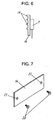
- the resin plate 14 Since the resin plate 14 has excellent processability, it is possible to integrally form holding portion 18 to hold electronic component on the resin plate 14 as shown in Fig. 5 and to integrally form heat dissipation fin 19 as shown in Fig. 6 and to make screw hole 21 for electronic component screw 20 as shown in Fig. 7.
- resin plate 14 and electronic equipment cover 22 are integrally molded.
- the heat dissipation area can be increased, and since the heat dissipation plate is facing the outermost portion of equipment, the heat dissipation effect will be enhanced in particular.
- the cover 22 As for integral molding, it is preferable to form the cover 22 by using resin with highly heat conductive material mixed in. As another method of molding, it is possible to form the resin plate 14 portion by using resin with highly heat conductive material mixed in and the cover 22 portion by using other molding resin, that is, to employ what is called a two-color molding method.
- connectors may be provided on the wiring board for connecting heat generating components previously bonded to the cover or to connect lead wires from heat generating components to another wiring board.
- the electronic equipment of the present invention comprises a wiring board, electronic component mounted on the wiring board, and an insulating heat dissipation plate thermally bonded to the electronic component, wherein the electronic component has a heat dissipation portion on the surface thereof, and the electronic component is bonded to the heat dissipation plate portion corresponding to the heat dissipation portion by using heat conductive bonding materials.
- the present invention it is unnecessary to dispose an insulating plate which is a thermal resistance between electronic component and heat dissipation plate, and it becomes possible to greatly enhance the heat dissipation effect of the heat generated from the electronic components.
Landscapes
- Engineering & Computer Science (AREA)
- Microelectronics & Electronic Packaging (AREA)
- Cooling Or The Like Of Electrical Apparatus (AREA)
- Cooling Or The Like Of Semiconductors Or Solid State Devices (AREA)
- Structures For Mounting Electric Components On Printed Circuit Boards (AREA)
Abstract
Description
- 1
- Wiring board
- 2
- Electrolytic capacitor
- 3
- Transformer
- 4
- Wiring module
- 5,6,7
- FET
- 8
- Diode
- 9
- Ceramic plate
- 10, 15, 16
- Land
- 11
- Mold resin
- 12
- Heat dissipation portion
- 13
- Clearance
- 14
- Resin plate
- 17
- Vent hole
- 18
- Holding portion
- 19
- Heat dissipation fin
- 20
- Screw
- 21
- Hole
- 22
- Cover
Claims (11)
- Electronic equipment comprising:wherein said heat dissipation portion is directly connected to said heat dissipation plate with heat conductive bonding material.a wiring board;an electronic component mounted on said wiring board and having a heat dissipation portion on a surface thereof; andan insulating heat dissipation plate thermally connected to said electronic component,
- The electronic equipment of claim 1, wherein said heat dissipation plate is a ceramic plate having at least one land for connecting said electronic component.
- The electronic equipment of claim 1, wherein said heat dissipation plates are disposed on said wiring board with a predetermined distance apart from each other.
- The electronic equipment of claim 1, wherein said heat dissipation plate is a resin plate containing a highly heat conductive material having at least one land for connecting said electronic component.
- The electronic equipment of claim 4, wherein said heat dissipation plates are disposed on said wiring board with a predetermined distance apart from each other.
- The electronic equipment of claim 4, wherein said heat dissipation plate further has a land for connecting electronic component other than the electronic component having a heat dissipation portion on a surface thereof.
- The electronic equipment of claim 4, wherein said heat dissipation plate further has a holding portion for holding electronic component.
- The electronic equipment of claim 4, wherein said heat dissipation plate further includes a heat dissipation fin portion integrally formed.
- The electronic equipment of claim 4, wherein said heat dissipation plate further has a vent hole.
- The electronic equipment of claim 4, wherein said heat dissipation plate further has a screw hole.
- The electronic equipment of claim 4, wherein said heat dissipation plate is unitary formed with an electronic equipment cover.
Applications Claiming Priority (6)
| Application Number | Priority Date | Filing Date | Title |
|---|---|---|---|
| JP2000283018 | 2000-09-19 | ||
| JP2000283018 | 2000-09-19 | ||
| JP2000242874 | 2001-08-09 | ||
| JP2001242874A JP4165045B2 (en) | 2000-09-19 | 2001-08-09 | Electronics |
| JP2001242874 | 2001-08-09 | ||
| PCT/JP2001/008053 WO2002025731A1 (en) | 2000-09-19 | 2001-09-17 | Electronic equipment |
Publications (3)
| Publication Number | Publication Date |
|---|---|
| EP1253636A1 true EP1253636A1 (en) | 2002-10-30 |
| EP1253636A8 EP1253636A8 (en) | 2003-03-12 |
| EP1253636A4 EP1253636A4 (en) | 2005-03-02 |
Family
ID=26600185
Family Applications (1)
| Application Number | Title | Priority Date | Filing Date |
|---|---|---|---|
| EP20010967704 Withdrawn EP1253636A4 (en) | 2000-09-19 | 2001-09-17 | ELECTRONIC EQUIPMENT |
Country Status (5)
| Country | Link |
|---|---|
| US (1) | US6753603B2 (en) |
| EP (1) | EP1253636A4 (en) |
| JP (1) | JP4165045B2 (en) |
| CN (1) | CN1200459C (en) |
| WO (1) | WO2002025731A1 (en) |
Cited By (2)
| Publication number | Priority date | Publication date | Assignee | Title |
|---|---|---|---|---|
| EP1589576A3 (en) * | 2004-04-20 | 2006-03-15 | Fujitsu Hitachi Plasma Display Limited | Heat dissipation in a drive circuit module for e.g. a plasma display device |
| EP1750490A1 (en) | 2005-08-02 | 2007-02-07 | Alcatel | Cooling of an electronic power device |
Families Citing this family (10)
| Publication number | Priority date | Publication date | Assignee | Title |
|---|---|---|---|---|
| JP4525648B2 (en) * | 2006-08-31 | 2010-08-18 | 船井電機株式会社 | Image forming apparatus |
| WO2008144856A2 (en) * | 2007-05-30 | 2008-12-04 | Techinvest Ltda | Constructive disposition in housing for the heat dissipation system and component installation in electric-electronic appliances |
| JP2009027043A (en) * | 2007-07-20 | 2009-02-05 | Tdk-Lambda Corp | Electronic component and its assembling method |
| DE202008005708U1 (en) * | 2008-04-24 | 2008-07-10 | Vishay Semiconductor Gmbh | Surface-mountable electronic component |
| JP5589979B2 (en) * | 2011-07-06 | 2014-09-17 | 株式会社豊田自動織機 | Circuit board |
| US9465049B2 (en) * | 2012-04-13 | 2016-10-11 | James B. Colvin | Apparatus and method for electronic sample preparation |
| DE102014000126A1 (en) * | 2014-01-13 | 2015-07-16 | Auto-Kabel Management Gmbh | Printed circuit board, circuit and method for producing a circuit |
| CN109152309A (en) * | 2018-10-19 | 2019-01-04 | 徐州携创智能科技有限公司 | A kind of electronic device |
| JP7696802B2 (en) * | 2021-09-29 | 2025-06-23 | 矢崎総業株式会社 | Heat sink and mounting board |
| CN116321991A (en) * | 2023-04-24 | 2023-06-23 | 台达电子企业管理(上海)有限公司 | Assembly Structure of Power Components |
Family Cites Families (17)
| Publication number | Priority date | Publication date | Assignee | Title |
|---|---|---|---|---|
| JPS58116235U (en) * | 1982-01-30 | 1983-08-08 | 松下電工株式会社 | Heat dissipation device for electronic components |
| JPS58116235A (en) | 1982-09-29 | 1983-07-11 | Nozawa Seisakusho:Kk | Self-propelling work bogie |
| DE3342923A1 (en) * | 1983-11-26 | 1985-06-05 | Philips Patentverwaltung Gmbh, 2000 Hamburg | Mounting system |
| US4853763A (en) * | 1984-06-27 | 1989-08-01 | The Bergquist Company | Mounting base pad means for semiconductor devices and method of preparing same |
| JPS6398135A (en) * | 1986-10-15 | 1988-04-28 | Matsushita Electric Ind Co Ltd | Printed substrate device for equipment |
| JPH0621589A (en) | 1992-07-06 | 1994-01-28 | Mitsubishi Materials Corp | Heat dissipating structure for hybrid ic and manufacture thereof |
| DE9300865U1 (en) * | 1993-01-22 | 1994-05-26 | Siemens AG, 80333 München | One-piece plastic part, especially injection molded part |
| JPH06275668A (en) | 1993-03-18 | 1994-09-30 | Fujitsu Ltd | Method for manufacturing semiconductor device having heat dissipation fin for cooling semiconductor element and resin composition for heat dissipation fin |
| JPH06283838A (en) * | 1993-03-26 | 1994-10-07 | Mitsubishi Electric Corp | Electronic circuit module |
| JPH08288438A (en) * | 1995-04-14 | 1996-11-01 | Hitachi Ltd | Electronic device cooling device |
| US5663529A (en) * | 1995-09-14 | 1997-09-02 | Ford Motor Company | Anti-skew mounting pads and processing method for electronic surface mount components |
| US5796584A (en) * | 1996-04-30 | 1998-08-18 | Telefonaktiebolaget Lm Ericsson | Bridge for power transistors with improved cooling |
| DE69727207T2 (en) * | 1996-09-09 | 2004-11-25 | Nec Tokin Corp., Sendai | HIGHLY CONDUCTING MAGNETIC MIXING MATERIAL |
| JPH10205861A (en) | 1997-01-18 | 1998-08-04 | Matsushita Electric Ind Co Ltd | Electronic control device of air conditioner |
| JPH10290086A (en) | 1997-04-15 | 1998-10-27 | Nemic Lambda Kk | Heat sink of electronic part |
| JPH11307968A (en) * | 1998-04-20 | 1999-11-05 | Matsushita Electric Ind Co Ltd | Heat dissipation structure of electronic control unit |
| JP2001185653A (en) * | 1999-10-12 | 2001-07-06 | Fujitsu Ltd | Semiconductor device and substrate manufacturing method |
-
2001
- 2001-08-09 JP JP2001242874A patent/JP4165045B2/en not_active Expired - Fee Related
- 2001-09-17 CN CN01802798.9A patent/CN1200459C/en not_active Expired - Fee Related
- 2001-09-17 EP EP20010967704 patent/EP1253636A4/en not_active Withdrawn
- 2001-09-17 US US10/130,210 patent/US6753603B2/en not_active Expired - Fee Related
- 2001-09-17 WO PCT/JP2001/008053 patent/WO2002025731A1/en not_active Ceased
Cited By (2)
| Publication number | Priority date | Publication date | Assignee | Title |
|---|---|---|---|---|
| EP1589576A3 (en) * | 2004-04-20 | 2006-03-15 | Fujitsu Hitachi Plasma Display Limited | Heat dissipation in a drive circuit module for e.g. a plasma display device |
| EP1750490A1 (en) | 2005-08-02 | 2007-02-07 | Alcatel | Cooling of an electronic power device |
Also Published As
| Publication number | Publication date |
|---|---|
| CN1393035A (en) | 2003-01-22 |
| CN1200459C (en) | 2005-05-04 |
| US20030057885A1 (en) | 2003-03-27 |
| JP2002171087A (en) | 2002-06-14 |
| WO2002025731A1 (en) | 2002-03-28 |
| EP1253636A8 (en) | 2003-03-12 |
| US6753603B2 (en) | 2004-06-22 |
| EP1253636A4 (en) | 2005-03-02 |
| JP4165045B2 (en) | 2008-10-15 |
Similar Documents
| Publication | Publication Date | Title |
|---|---|---|
| US5345106A (en) | Electronic circuit component with heat sink mounted on a lead frame | |
| EP1439587B1 (en) | Mounting of an LED assembly with self-alignment | |
| US7919854B2 (en) | Semiconductor module with two cooling surfaces and method | |
| US6377462B1 (en) | Circuit board assembly with heat sinking | |
| EP0521343B1 (en) | Electronic device and its production method | |
| US6753603B2 (en) | Electronic equipment having insulating heat dissipation plate | |
| JPS6333320B2 (en) | ||
| KR100421301B1 (en) | Polymer stud-matrix housing for microwave circuit arrangements | |
| US7688591B2 (en) | Electronic-component-mounting board | |
| WO2005083807A1 (en) | A pcb-mounted radiator and an led package using the pcb, and the manufacturing method thereof | |
| KR100430325B1 (en) | Polymer stud grid array | |
| US7049171B2 (en) | Electrical package employing segmented connector and solder joint | |
| US5739743A (en) | Asymmetric resistor terminal | |
| US5468909A (en) | Insulating part with improved heat transfer element | |
| CN119181678B (en) | Package structure | |
| JPH0812895B2 (en) | Semiconductor device mounted pin grid array package substrate | |
| JPH11288803A (en) | Surface mounted thermistor component | |
| JP2001223452A (en) | Circuit board | |
| JPH0587982U (en) | Hybrid integrated circuit device having heat generating components | |
| JP7548089B2 (en) | Circuit device | |
| JP2006004987A (en) | Package for optical semiconductor element and light emitting device using the same | |
| JPH04142068A (en) | Electronical component mounting board and manufacture thereof | |
| EP1739741A2 (en) | Electronic assembly with backplate having at least one thermal insert | |
| JPH0518862Y2 (en) | ||
| JPH07226454A (en) | Semiconductor device |
Legal Events
| Date | Code | Title | Description |
|---|---|---|---|
| PUAI | Public reference made under article 153(3) epc to a published international application that has entered the european phase |
Free format text: ORIGINAL CODE: 0009012 |
|
| 17P | Request for examination filed |
Effective date: 20020517 |
|
| AK | Designated contracting states |
Kind code of ref document: A1 Designated state(s): AT BE CH CY DE DK ES FI FR GB GR IE IT LI LU MC NL PT SE TR |
|
| RBV | Designated contracting states (corrected) |
Designated state(s): AT BE CH DE FR GB LI |
|
| A4 | Supplementary search report drawn up and despatched |
Effective date: 20050119 |
|
| RIC1 | Information provided on ipc code assigned before grant |
Ipc: 7H 01L 23/373 B Ipc: 7H 01L 23/40 A Ipc: 7H 01L 23/36 B |
|
| 17Q | First examination report despatched |
Effective date: 20070222 |
|
| RAP1 | Party data changed (applicant data changed or rights of an application transferred) |
Owner name: PANASONIC CORPORATION |
|
| STAA | Information on the status of an ep patent application or granted ep patent |
Free format text: STATUS: THE APPLICATION IS DEEMED TO BE WITHDRAWN |
|
| 18D | Application deemed to be withdrawn |
Effective date: 20120403 |