EP1253507A2 - Processor and reset control method for the processor - Google Patents
Processor and reset control method for the processor Download PDFInfo
- Publication number
- EP1253507A2 EP1253507A2 EP01309804A EP01309804A EP1253507A2 EP 1253507 A2 EP1253507 A2 EP 1253507A2 EP 01309804 A EP01309804 A EP 01309804A EP 01309804 A EP01309804 A EP 01309804A EP 1253507 A2 EP1253507 A2 EP 1253507A2
- Authority
- EP
- European Patent Office
- Prior art keywords
- initial setting
- setting area
- input
- flag
- reset signal
- Prior art date
- Legal status (The legal status is an assumption and is not a legal conclusion. Google has not performed a legal analysis and makes no representation as to the accuracy of the status listed.)
- Granted
Links
Images


Classifications
-
- G—PHYSICS
- G06—COMPUTING OR CALCULATING; COUNTING
- G06F—ELECTRIC DIGITAL DATA PROCESSING
- G06F1/00—Details not covered by groups G06F3/00 - G06F13/00 and G06F21/00
- G06F1/24—Resetting means
Definitions
- the present invention relates to a processor, and a reset control method for that processor, which can be used in a portable terminal, portable telephone, or digital camera.
- processors are provided with the function of setting appropriate states for processors and for systems formed from those processors by generating reset interruptions using reset signals and executing system initialization programs.
- a reset signal is input from the outside as a result of the pressing of a reset button or of the input of power
- an activation reset operation is executed so as to initialize the storage element inside the processor.
- reset interruption is generated inside the processor and a program for initialization processing known as a reset vector is read from ROM (Read Only Memory) connected to the exterior of the processor via a bus.
- ROM Read Only Memory
- the processor in order to achieve lower power consumption in the processor, if there is no processing deemed to be indispensable being executed in the processor for a set length of time, the processor is provided with a function of stopping the supply of clocks to the processor. In a processor having this type of function, in order to restart the operation of the processor after the clocks have been stopped, it is normal for a reset signal to be input once again.
- the ROM is a low speed memory device
- an area in which initial settings are to be made by a reset signal is divided into, for example, a first initial setting area comprising a register group that is essential in order to perform communication between the processor and outside the processor; a second initial setting area that comprises the remainder of the area excluding the register group of the first initial setting area and a register group concerned with the execution of instructions within the processor; and a third initial setting area comprising the register group concerned with the execution of instructions within the processor.
- the first initial setting area initial settings are made on the basis of a first reset signal.
- the second initial setting area initial settings are made on the basis of either the first reset signals or second reset signals.
- initial settings are made on the basis of either the first reset signals, the second reset signals, or third reset signals.
- first, second, and third flags are provided to correspond respectively to the first, second, and third initial setting area. All the flags are cleared by the first reset signal. The remaining flags apart from the first flags are cleared by the second reset signal. The third flags only are cleared by the third reset signal.
- the first flag is set.
- the second flag and the third flag are set respectively.
- initial settings are made for the processor as a whole by the first reset signal.
- Initial settings are made for the area excluding the register group that is essential for performing communication between the processor and outside the processor by the second reset signal.
- initial settings are made only for the register group involved with the execution of instructions within the processor by the third reset signal.
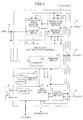
- Fig. 1 is a block diagram showing the structure of the main portions of the processor according to the embodiment of the present invention.
- the processor 1 is provided with an instruction fetching control section 11, instruction control section 12, cache unit 13 comprising cache memory and a cache control section, bus control section 14, clock control section 15, first register group 16, reset register (RSTR) 2, and a setting completion display register (RSTCR) 3.
- instruction fetching control section 11 instruction control section 12
- cache unit 13 comprising cache memory and a cache control section
- bus control section 14 clock control section
- first register group 16 reset register (RSTR) 2 reset register
- RSTCR setting completion display register
- third, and fourth register groups 41, 42, and 43 each formed from one or two or more registers are provided respectively in the instruction fetching control section 11, the instruction control section 12, and the cache unit 13.
- a pair of registers (ASR and AMR) 45 for setting comparative inhibited bits and start addresses of the address range of the RAM 5 forming the local memory for the processor 1 is also provided in the bus control section 14.
- the processor 1 is connected to unillustrated ROM via an address bus and a data bus controlled by the bus control section 14. Note that, in Fig. 1, those structural portions that are not related to the present invention have not been shown.
- the first register group 16 and the address setting register 45 for the RAM 5 (local memory) represented by ASR and AMR are the object of the initial setting processing when a PRST signal, which is the first reset signal, is generated.
- the other registers provided in the bus control section 14 are the objects of the initial setting processing when a PRST signal or an HRST signal, which is the second reset signal, is generated.
- the second, third, and fourth register groups 41, 42, and 43 are the objects of the initial setting processing when a PRST signal, an HRST signal, or an SRST signal, which is the third reset signal, is generated.
- the first register group 16 when a PRST signal is generated, the first register group 16, the address setting register 45 represented by ASR and AMR, registers other than the address setting register 45 represented by ASR and AMR from among the registers provided in the bus control section 14, and the second, third, and fourth register groups 41, 42, and 43 are the objects of the initial setting processing.
- the registers other than the address setting register 45 represented by ASR and AMR from among the registers provided in the bus control section 14, and the second, third, and fourth register groups 41, 42, and 43 are the objects of the initial setting processing.
- those registers (not illustrated) that have stopped the supply of the clocks to the interior of the processor in the clock control section 15 are also reset as a result of the generation of an HRST signal.
- the clock control section 15 restarts the supply to each section of the processor of clocks that are supplied from the outside.
- the first register group 16 and the address setting register 45 represented by ASR and AMR correspond to the first initial setting area.
- the registers other than the address setting register 45 represented by ASR and AMR from among the registers provided in the bus control section 14 correspond to the second initial setting area.
- the second, third, and fourth register groups 41, 42, and 43 correspond to the third initial setting area.
- the symbol 17 indicates the terminal by which the PRST signals are input from the outside (i.e. the PRST terminal); the symbol 18 indicates the terminal by which the HRST signals are input from the outside (i.e. the HRST terminal); and the symbol 19 indicates the terminal by which the SRST signals are input from the outside (i.e. the SRST terminal).
- the symbol 10 indicates the terminal by which the clocks are input from the outside (i.e. the CLOCK terminal).
- Fig. 2 is a table showing an example of a register contained in the first initial setting area.
- ARS0 to ARS3 are DRAM address area setting registers.
- AMK0 to AMK3 are DRAM address mask registers.
- DCTL is a DRAM control register for performing the setting of the minimum number of cycles during the DRAM operations that is different for each type of DRAM.
- DAMC is a DRAM access mode control register for selecting a mode for accessing DRAM.
- DCFG is a DRAM configuration register for performing the display and settings of DRAM type, bus width of the DRAM bus, DRAM direct coupling/DIM use, and the like.
- DAN is a DRAM address number register for setting the RAS address bit number of DRAM connected to four DCS, the CAS address bit number, and the bank address bit number.
- DSTS is a DRAM status register showing the state of the SDRAM controller.
- DRCN is a DRAM refresh control register for supporting auto-refresh and self-refresh as SDRAM refresh.
- DART is a DRAM auto-refresh time register for stipulating the refresh intervals during auto-refresh.
- DARS DRAM address area setting register
- DAMK DRAM address mask register
- the DRAM is the RAM 5 forming the local memory of the processor 1.
- Fig. 3 is a schematic view showing the structure of the reset register 2.
- the reset register 2 is provided with an HS bit 21 and an SS bit 22. Signals that are the equivalent of HRST signals, which are reset signals input from the HRST terminal 18, are asserted inside the processor 1 by writing to the HS bit 21. In addition, signals that are the equivalent of SRST signals, which are reset signals input from the SRST terminal 19, are asserted inside the processor 1 by writing to the SS bit 22.
- Fig. 4 is a circuit diagram showing the structure of the initialization control section of the processor 1. Note that this initialization control section is omitted in Fig. 1. PRST signals input from the outside via the PRST terminal 17 are supplied as they are to the interior of the processor 1.
- SRST signals input from the outside via the SRST terminal 19 (referred to below as external SRST signals) and the signals that are equivalent to the external SRST signals (referred to below as internal SRST signals) that are generated by writing to the SS bit 22 of the reset register 2.
- write signals to the SS bit 22 are supplied to a shift register formed from a plurality of flip-flops 73, 74, 75, etc.
- the output signals at the various stages of this shift register are supplied via a NOR circuit 76 to the enable terminal (EN) of the flip-flop 72 into which the write signals to the SS bit 22 are input.
- NOR circuit 76 to the enable terminal (EN) of the flip-flop 72 into which the write signals to the SS bit 22 are input.
- internal SRST signals are being continually generated until the shifting of the write signals to the SS bit 22 in the shift register is ended.
- These internal SRST signals and external SRST signals are input into an OR circuit 71 and are asserted.
- Fig. 5 is a schematic view showing the structure of the setting completion display register 3.
- the setting completion display register 3 is provided with a PC bit 31, an HC bit 32, and an SC bit 33.
- the PC bit 31 houses a first flag.
- the first flag indicates whether or not the initial setting processing of the first initial setting area is completed.
- the HC bit 32 houses a second flag.
- the second flag indicates whether or not the initial setting processing of the second initial setting area is completed.
- the SC bit 33 houses a third flag.
- the third flag indicates whether or not the initial setting processing of the third initial setting area is completed.
- PRST signals and also output signals from an OR circuit 85 that inputs either an internal or an external HRST signal are input into the reset terminal of the flip-flop 82 of the HC bit 32.
- Signals generated by the completion of the initial setting processing of the second initial setting processing area namely, signals for setting the second flag of the HC bit 32 (referred to below as HC set signals) are input via an OR circuit 86 to the input terminal of the flip-flop 82.
- Output signals from the flip-flop 82 are also input into the OR circuit 86. Accordingly, the HC bit 32 is reset when a PRST signal or an external or internal HRST signal is asserted.
- an HC set signal is input, a state in which the flag is set is maintained until the next PRST signal or external or internal HRST signal is asserted.
- PRST signals, internal or external HRST signals, and also output signals from an OR circuit 87 that inputs either an internal or an external SRST signal are input into the reset terminal of the flip-flop 83 of the SC bit 33.
- Signals generated by the completion of the initial setting processing of the third initial setting processing area, namely, signals for setting the third flag of the SC bit 33 (referred to below as SC set signals) are input via an OR circuit 88 to the input terminal of the flip-flop 83.
- Output signals from the flip-flop 83 are also input into the OR circuit 88. Accordingly, the SC bit 33 is reset when a PRST signal, an internal or external HRST signal, or an internal or external SRST signal is asserted.
- the SC bit 33 When an SC set signal is input, the SC bit 33 maintains a state in which the flag is set until the next PRST signal, internal or external HRST signal, or internal or external SRST signal is asserted. Note that, if the hardware of the processor 1 has a function for automatically generating an initialization sequence, the PC bit 31, the HC bit 32, and the SC bit 33 are automatically set at the completion of this setting sequence. The PC bit 31, the HC bit 32, and the SC bit 33 are set by reset signals that perform the initialization of the corresponding sequencer portions.
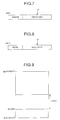
- Fig. 7 and Fig. 8 are schematic views respectively showing the structures of a register (ASR) 46 for setting a start address and a register (AMR) 47 for setting a comparative inhibited bit of a pair of registers (ASR and AMR) 45 for setting a comparative inhibited bit and start address of an address range of the RAM 5, which is the local memory for the processor 1.
- Fig. 9 is a view of a memory map schematically showing the addresses assigned to the RAM 5 based on the register (AMR) 47 for setting the comparative inhibited bits and the register (ASR) 46 for setting the start address. Out of those addresses set by the register (ASR) 46 for setting the start address, an address represented by upper order bits that are not masked by the register (AMR) 47 for setting the comparative inhibited bits becomes the address for the area of the RAM 5.
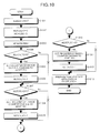
- step S1001 when a PRST signal is asserted (step S1001), the PC bit 31, the HC bit 32, and the SC bit 33 of the setting completion display register (RSTCR) 3 are reset to "0", for example (step S1002). Thereafter, when the PRST signal is negated (step S1003), a request to fetch an instruction is issued from the initial address, for example, "0xFF00_0000". Because effective data is not held in the RAM 5 immediately after the power has been supplied, the processor 1 accesses ROM on an external bus.
- the initialization program housed in the ROM checks the value of the PC bit 31 (step S1004) and confirms that that value is "0", for example, (step S1004: YES). As a result, a routine that includes the processing needed when a PRST signal is asserted is executed.
- the address information for accessing the RAM 5 is set, for example, in the register (AMR) 47 for setting the comparative inhibited bits of the address range and the register (ASR) 46 for setting the start address of the address range.
- step S1005 the initialization program performs the writing to the PC bit 31 and sets this bit, for example, to "1" (step S1006).
- the initialization program refers to the value of the HC bit 32 (step S1007). Because the HC bit 32 is reset in step S1002, naturally, the value of the HC bit 32 is "0" (step S1007: YES). Accordingly, a routine that includes the processing needed when an external or internal HRST signal is asserted is executed and the setting of the registers included in the second initial setting area is completed (step S1008). Next, the initialization program performs the writing to the HC bit 32 and sets this bit to "1", for example (step S1009).
- the initialization program refers to the value of the SC bit 33 (step S1010).
- the value of the SC bit 33 is "0" (step S1010: YES).
- a routine that includes the processing needed when an external or internal SRST signal is asserted is executed and the setting of the registers included in the third initial setting area is completed (step S1011).
- the initialization program performs the writing to the SC bit 33 and sets this bit to "1", for example (step S1012).
- the preparation to start the application is completed (step S1013).
- the register stopping the clocks in the clock control section 15 is reset and the supply of clocks to the interior of the processor 1 is started.
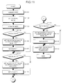
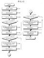
- the HC bit 32, and the SC bit 33 of the setting completion display register (RSTCR) 3 are reset to "0", for example (step S1102).
- the reset operation is not performed for the PC bit 31. Accordingly, in the RAM 5, the effective data remains in a held state.
- step S1103 when the external HRST signal is negated (step S1103), the initialization program stored in the RAM 5 refers to the value of the PC bit 31 (step S1104). If the value of the PC bit 31 is "1" (step S1104: NO), because all of the registers contained in the first initial setting area are in a state in which they have been set, the initial setting processing for the first initial setting area (i.e. steps S1105 and S1106) are omitted.
- the initialization program refers to the value of the HC bit 32 (step S1107).
- the registers contained in the second initial setting area are set (step S1108) and the value of the HC bit 32 is set to "1" (step S1109).
- the initialization program refers to the value of the SC bit 33 (step S1110). Because the value of the SC bit 33 is also naturally "0" (step S1110: YES), the registers contained in the third initial setting area are set (step S1111) and thereafter the value of the SC bit 33 is set to "1" (step S1112). As a result of the above processing, the preparation to start the application is completed (step S1113). Note that the reactivation sequence shown in Fig. 11 is the same as that when an internal HRST signal is activated.
- the reason for referring to the value of the PC bit 31 in step S1104 is because if an internal HRST signal or an internal HRST signal is asserted during the initialization sequence shown in Fig. 10 as a result, for example, of the assertion of a PRST signal before the initial setting processing of the first initial setting area has been completed, then it is necessary to complete the initial setting processing of the first initial setting area.
- the processor 1 of the present embodiment being provided with the setting completion display register (RSTCT) 3 and having a structure in which it is able to discover whether or not the initial setting processing of each initial setting area has been completed by referring to this register.
- the structure is one that does not have the setting completion display register (RSTCR) 3 provided but instead has provided a plurality of reset signals and a plurality of initial setting areas to correspond with the respective reset signals, and initial setting processing of the areas that correspond to the asserted reset signals is performed, then if external HRST signals or internal HRST signals are asserted during the execution of the initialization sequence as a result of the assertion of the PRST signals, in some cases the initial setting processing of the second and third initial setting area is completed without the initial setting of the first initial setting area being performed to its completion. In other words, the problem occurs that the processor 1 does not reach a fully activated state.
- RSTCR setting completion display register
- step S1201 when an external or internal SRST signal is asserted (step S1201), the registers in the instruction fetch control section 11, the instruction execution section 12, and the cache unit 13 are all initialized.
- step S1202 the SC bit 33 of the setting completion display register (RSTCR) 3 is reset to "0", for example (step S1202). At this time, the reset operations for the PC bit 31 and the HC bit 32 are not performed.
- step S1203 When the internal or external SRST signal is negated (step S1203), a request to fetch an instruction is issued from the initial address "0xFF00_0000".
- the initialization program housed in the RAM 5 refers the value of the PC bit 31 (step S1204) and if that value is "1" (step S1204: NO), then because the registers contained in the first initial setting area are all in a set state, the initial setting processing (steps S1205 and S1206) are omitted for the first initial setting area.
- step S1210 Continuing on the initialization program refers to the value of the SC bit 33 (step S1210).
- the value of the SC bit 33 is "0" (step S1210: YES).
- step S1211 the registers contained in the third initialization area are set (step S1211) and thereafter the value of the SC bit 33 is set to "1" (step S1212).
- step S1213 the preparation to start the application is completed (step S1213).
- step S1202 regardless of whether or not the PC bit 31 and the HC bit 32 of the setting completion display register (RSTCR) 3 are reset in step S1202, the reason for referring to the value of the PC bit 31 in step S1204 and to the value of the HC bit 32 in step S1207 is so as to prevent the same problems that arise if an internal HRST signal or an internal HRST signal is asserted during the initialization sequence by a PRST signal.
- step S1204 if, as a result of referring to the value of the PC bit 31 in step S1204, that value is found to be a reset value (step S1204: YES), the initial setting processing for the first initial setting area is performed (step S1205) and, after the value of the PC bit 31 has been set (step S1206), the routine moves to step S1207.
- step S1207 the value of the HC bit 32 is referred to and if that value is a reset value (step S1207: YES), the initial setting processing for the second initial setting area is performed (step S1208) and, after the value of the HC bit 32 has been set (step S1209), the routine moves to step S1210.
- the first initial setting area, the second initial setting area, and the third initial setting area are initially set by a PRST signal; the second initial setting area, and the third initial setting area are initially set by an external HRST signal or internal HRST signal; and the third initial setting area is initially set by an external SRST signal or internal SRST signal.
- the present invention in the above description is not limited to the above embodiment and may be altered in a variety of ways.
- the number of initial setting areas is not limited to three and two or four or more initial setting areas are possible.
- which register is contained in which initial setting area is also optional.
- a processor as a whole is initially set using a first reset signal.
- An area other than a register group that is essential for performing communication between a processor and the outside of the processor is initially set using a second reset signal.
- only the register group involved with the execution of instructions within the processor is initially set using a third reset signal. Therefore, when the second reset signal is generated it is possible to omit the initial setting of the register group that is necessary for performing communication between a processor and the outside of the processor.
- the third reset signal it is possible to omit the initial setting of areas other than the register group involved with the execution of instructions within the processor. As a result, when the second or third reset signal is generated, it is possible to bring the processor back to an operating state extremely rapidly from a stopped state.
Landscapes
- Engineering & Computer Science (AREA)
- Theoretical Computer Science (AREA)
- Physics & Mathematics (AREA)
- General Engineering & Computer Science (AREA)
- General Physics & Mathematics (AREA)
- Microcomputers (AREA)
- Multi Processors (AREA)
- Retry When Errors Occur (AREA)
Abstract
Description
Claims (11)
- A processor comprising:a first initial setting area which is initialized based on an input of a first reset signal;a second initial setting area which is initialized based on an input of either the first reset signal or a second reset signal and which does not overlap with said first initial setting area;a first flag that is cleared by an input of the first reset signal and that is set when initial setting of the first initial setting area has been completed; anda second flag that is cleared by an input of either the first or second reset signals and that is set when initial setting of the second initial setting area has been completed, whereinwhen either one of the first and second reset signals is input, initial setting area/s corresponding to cleared flag/s is/are initialized out of the first and second initial setting areas.
- The processor according to claim 1, further comprising:a third initial setting area which is initialized based on an input of the first or second reset signals or a third input signal and which does not overlap with both said first initial setting area and said second initial setting area; anda third flag that is cleared by an input of any one of the first through third reset signals and that is set when initial setting of the third initial setting area has been completed, whereinwhen any one of the first through third reset signals is input, initial setting area/s corresponding to cleared flag/s is/are initialized out of the first through third initial setting areas.
- The processor according to claim 2, wherein
the first initial setting area is formed by a first register group for performing communication between the processor and outside the processor,
the third initial setting area is formed by a second register group relating to execution of instructions inside the processor, and
the second initial setting area is an area other than both the first register group and the second register group. - The processor according to claim 2 or 3, further comprising:an n-th initial setting area, where n is an integer having value equal to or more than 4, which does not overlap with each initial setting area from the first initial setting area through an (n-1)-th initial setting area and which is initialized based on an input of the first reset signal through an n-th reset signal different from any of the first through an (n-1)-th reset signal; andan n-th flag that is cleared by an input of any of the first reset signal through the n-th reset signal and that is set when initial setting of the n-th initial setting area has been completed, whereinwhen any one of the first through n-th reset signals is input, initial setting area/s corresponding to cleared flag/s is/are initialized out of the first through n-th initial setting areas.
- The processor according to any preceding claim, wherein the processor is provided with an external input terminal for receiving the respective reset signals from the outside.
- The processor according to any of claims 1 to 4, wherein the respective reset signals are generated within the processor.
- A method of controlling resetting of a processor, the processor including
a first initial setting area which is initialized based on an input of a first reset signal;
a second initial setting area which is initialized based on an input of either the first reset signal or a second reset signal and which does not overlap with said first initial setting area;
a first flag that is cleared by an input of the first reset signal and that is set when initial setting of the first initial setting area has been completed; and
a second flag that is cleared by an input of either the first or second reset signals and that is set when initial setting of the second initial setting area has been completed, wherein
when either one of the first and second reset signals is input, initial setting area/s corresponding to cleared flag/s is/are initialized out of the first and second initial setting areas,
the method comprising:a step in which flags that correspond to each reset signal type are cleared; anda step in which a state of each flag is confirmed, initial setting is performed for an initial setting area corresponding to the cleared flags and, after the initial setting is completed, setting corresponding flags is repeatedly performed until all of the flags are placed in a set state. - A method of controlling resetting of a processor, the processor including
a first initial setting area which is initialized based on an input of a first reset signal;
a second initial setting area which is initialized based on an input of either the first reset signal or a second reset signal and which does not overlap with said first initial setting area;
a first flag that is cleared by an input of the first reset signal and that is set when initial setting of the first initial setting area has been completed; and
a second flag that is cleared by an input of either the first or second reset signals and that is set when initial setting of the second initial setting area has been completed, wherein
when either one of the first and second reset signals is input, initial setting area/s corresponding to cleared flag/s is/are initialized out of the first and second initial setting areas,
the method comprising the steps of:clearing the first flag if the first reset signal is received, and clearing the first and second flags if the second reset signal is received;checking which flag/s has/have been cleared out of the first and second flags;initializing initial setting area/s corresponding to the cleared flag/s out of the first and second areas, andsetting flag/s corresponding to the initial setting area/s which has/have been initialized out of the first and second areas. - A method of controlling resetting of a processor, the processor including
a first initial setting area which is initialized based on an input of a first reset signal;
a second initial setting area which is initialized based on an input of either the first reset signal or a second reset signal and which does not overlap with said first initial setting area;
a third initial setting area which is initialized based on an input of the first or second reset signals or a third input signal and which does not overlap with both said first initial setting area and said second initial setting area;
a first flag that is cleared by an input of the first reset signal and that is set when initial setting of the first initial setting area has been completed;
a second flag that is cleared by an input of either the first or second reset signals and that is set when initial setting of the second initial setting area has been completed, and
a third flag that is cleared by an input of any one of the first through third reset signals and that is set when initial setting of the third initial setting area has been completed, wherein
when any one of the first through third reset signals is input, initial setting area/s corresponding to cleared flag/s is/are initialized out of the first through third initial setting areas,
the method comprising the steps of :clearing the first flag if the first reset signal is received, clearing the first and second flags if the second reset signal is received, and clearing the first through third flags if the third reset signal is received;checking which flag/s has/have been cleared out of the first through third flags;initializing initial setting area/s corresponding to the cleared flag/s out of the first through third areas, andsetting flag/s corresponding to the initial setting area/s which has/have been initialized out of the first through third areas. - The method of controlling resetting of a processor according to claim 9, wherein
the first initial setting area is formed by a first register group for performing communication between the processor and outside the processor,
the third initial setting area is formed by a second register group relating to the execution of instructions inside the processor, and
the second initial setting area is an area other than both the first register group and the second register group. - A method of controlling resetting of a processor, the processor including
a first initial setting area which is initialized based on an input of a first reset signal;
a second initial setting area which is initialized based on an input of either the first reset signal or a second reset signal and which does not overlap with said first initial setting area;
a third initial setting area which is initialized based on an input of the first or second reset signals or a third input signal and which does not overlap with both said first initial setting area and said second initial setting area;
an n-th initial setting area, where n is an integer having value equal to or more than 4, which does not overlap with each initial setting area from the first initial setting area through an (n-1)-th initial setting area and which is initialized based on an input of the first reset signal through an n-th reset signal different from any of the first through an (n-1)-th reset signal;
a first flag that is cleared by an input of the first reset signal and that is set when initial setting of the first initial setting area has been completed;
a second flag that is cleared by an input of either the first or second reset signals and that is set when initial setting of the second initial setting area has been completed;
a third flag that is cleared by an input of any one of the first through third reset signals and that is set when initial setting of the third initial setting area has been completed, and
an n-th flag that is cleared by an input of any of the first reset signal through the n-th reset signal and that is set when initial setting of the n-th initial setting area has been completed, wherein
when any one of the first through n-th reset signals is input, initial setting area/s corresponding to cleared flag/s is/are initialized out of the first through n-th initial setting areas,
the method comprising the steps of:clearing the first flag if the first reset signal is received, clearing the first and second flags if the second reset signal is received, clearing the first through third flags if the third reset signal is received, and clearing the first through n-th flags if the n-th reset signal is received;checking which flag/s has/have been cleared out of the first through n-th flags;initializing initial setting area/s corresponding to the cleared flag/s out of the first through n-th areas, andsetting flag/s corresponding to the initial setting area/s which has/have been initialized out of the first through n-th areas.
Applications Claiming Priority (2)
| Application Number | Priority Date | Filing Date | Title |
|---|---|---|---|
| JP2001129781 | 2001-04-26 | ||
| JP2001129781A JP4443067B2 (en) | 2001-04-26 | 2001-04-26 | Processor and reset control method thereof |
Publications (3)
| Publication Number | Publication Date |
|---|---|
| EP1253507A2 true EP1253507A2 (en) | 2002-10-30 |
| EP1253507A3 EP1253507A3 (en) | 2004-06-16 |
| EP1253507B1 EP1253507B1 (en) | 2009-03-11 |
Family
ID=18978261
Family Applications (1)
| Application Number | Title | Priority Date | Filing Date |
|---|---|---|---|
| EP01309804A Expired - Lifetime EP1253507B1 (en) | 2001-04-26 | 2001-11-21 | Processor and reset control method for the processor |
Country Status (4)
| Country | Link |
|---|---|
| US (1) | US6963969B2 (en) |
| EP (1) | EP1253507B1 (en) |
| JP (1) | JP4443067B2 (en) |
| DE (1) | DE60137912D1 (en) |
Families Citing this family (4)
| Publication number | Priority date | Publication date | Assignee | Title |
|---|---|---|---|---|
| DE10161295A1 (en) * | 2001-12-13 | 2003-07-03 | Siemens Ag | Method for avoiding total failure of a processing unit for protocol information |
| US8214592B2 (en) * | 2009-04-15 | 2012-07-03 | International Business Machines Corporation | Dynamic runtime modification of array layout for offset |
| US9111632B2 (en) * | 2010-07-29 | 2015-08-18 | Renesas Electronics Corporation | Semiconductor device and data processing system with coordinated calibration and refresh operations |
| US11074960B2 (en) * | 2019-06-17 | 2021-07-27 | Micron Technology, Inc. | Interrupt-driven content protection of a memory device |
Family Cites Families (10)
| Publication number | Priority date | Publication date | Assignee | Title |
|---|---|---|---|---|
| US4688212A (en) * | 1985-01-31 | 1987-08-18 | Harris Corporation | Centralized image responsive telephone time slot interchange system |
| DE3886529T2 (en) * | 1988-08-27 | 1994-06-30 | Ibm | Establishment in a data processing system for system initialization and reset. |
| US5321830A (en) * | 1990-04-13 | 1994-06-14 | Fujitsu Limited | Reset method when adaptor module is faulty and computer system executing same |
| GB9024488D0 (en) * | 1990-11-10 | 1991-01-02 | Lucas Ind Plc | Improvements in and relating to microprocessor based systems |
| US5315184A (en) * | 1992-05-04 | 1994-05-24 | Zilog, Inc. | Self arbitrating auto resettable flag circuit |
| US5860125A (en) * | 1995-11-08 | 1999-01-12 | Advanced Micro Devices, Inc. | Integrated circuit including a real time clock, configuration RAM, and memory controller in a core section which receives an asynchronous partial reset and an asynchronous master reset |
| DE19612440C1 (en) * | 1996-03-28 | 1997-05-07 | Siemens Ag | Control circuit e.g. for individual register of semiconductor memory on microprocessor chip |
| US6400715B1 (en) * | 1996-09-18 | 2002-06-04 | Texas Instruments Incorporated | Network address matching circuit and method |
| KR100209762B1 (en) * | 1996-10-28 | 1999-07-15 | 구본준 | Reset apparatus and operation mode regulating method using its |
| US6314501B1 (en) * | 1998-07-23 | 2001-11-06 | Unisys Corporation | Computer system and method for operating multiple operating systems in different partitions of the computer system and for allowing the different partitions to communicate with one another through shared memory |
-
2001
- 2001-04-26 JP JP2001129781A patent/JP4443067B2/en not_active Expired - Fee Related
- 2001-11-06 US US09/985,766 patent/US6963969B2/en not_active Expired - Lifetime
- 2001-11-21 EP EP01309804A patent/EP1253507B1/en not_active Expired - Lifetime
- 2001-11-21 DE DE60137912T patent/DE60137912D1/en not_active Expired - Lifetime
Also Published As
| Publication number | Publication date |
|---|---|
| EP1253507A3 (en) | 2004-06-16 |
| US20020161992A1 (en) | 2002-10-31 |
| DE60137912D1 (en) | 2009-04-23 |
| JP2002328751A (en) | 2002-11-15 |
| EP1253507B1 (en) | 2009-03-11 |
| JP4443067B2 (en) | 2010-03-31 |
| US6963969B2 (en) | 2005-11-08 |
Similar Documents
| Publication | Publication Date | Title |
|---|---|---|
| JPH0368476B2 (en) | ||
| JPH0346850B2 (en) | ||
| KR920005739B1 (en) | Partial write control circuits used for memory units. | |
| EP1253507B1 (en) | Processor and reset control method for the processor | |
| JP2548428B2 (en) | Timing generator | |
| JPS5911921B2 (en) | numerical control device | |
| KR102753546B1 (en) | Semiconductor device and method for operating the same | |
| US6205539B1 (en) | Method for manipulating a stack pointer with post increment/decrement operation | |
| JP2003233509A (en) | Digital signal processor | |
| US20010003201A1 (en) | Pre-decoded stack pointer with post increment /decrement operation | |
| JPH10144073A (en) | Access mechanism for synchronous DRAM | |
| JP4071930B2 (en) | Synchronous DRAM | |
| JP3438503B2 (en) | Display control device | |
| CN116204584B (en) | A method, apparatus, readable storage medium, and electronic device for writing logs. | |
| JP3222647B2 (en) | Automatic memory bank switching system | |
| JP2570900B2 (en) | Access control device and access control method | |
| JP2000029508A (en) | Programmable controller | |
| JP3255429B2 (en) | Memory interface circuit | |
| KR100491861B1 (en) | memory control method for realizing zero wait accessing to synchronous memory buit-in MCU with ARM core | |
| SU1124275A1 (en) | Microprocessor communication device | |
| JPH087562A (en) | Dynamic random access memory | |
| JP2919357B2 (en) | CPU interface circuit | |
| JPS6215645A (en) | Central processing unit | |
| JPH03259338A (en) | Information processor | |
| JP2002024080A (en) | RAM reset method and RAM interface circuit |
Legal Events
| Date | Code | Title | Description |
|---|---|---|---|
| PUAI | Public reference made under article 153(3) epc to a published international application that has entered the european phase |
Free format text: ORIGINAL CODE: 0009012 |
|
| AK | Designated contracting states |
Kind code of ref document: A2 Designated state(s): AT BE CH CY DE DK ES FI FR GB GR IE IT LI LU MC NL PT SE TR |
|
| AX | Request for extension of the european patent |
Free format text: AL;LT;LV;MK;RO;SI |
|
| PUAL | Search report despatched |
Free format text: ORIGINAL CODE: 0009013 |
|
| AK | Designated contracting states |
Kind code of ref document: A3 Designated state(s): AT BE CH CY DE DK ES FI FR GB GR IE IT LI LU MC NL PT SE TR |
|
| AX | Request for extension of the european patent |
Extension state: AL LT LV MK RO SI |
|
| 17P | Request for examination filed |
Effective date: 20041208 |
|
| AKX | Designation fees paid |
Designated state(s): DE FR GB |
|
| 17Q | First examination report despatched |
Effective date: 20080606 |
|
| GRAP | Despatch of communication of intention to grant a patent |
Free format text: ORIGINAL CODE: EPIDOSNIGR1 |
|
| GRAS | Grant fee paid |
Free format text: ORIGINAL CODE: EPIDOSNIGR3 |
|
| GRAA | (expected) grant |
Free format text: ORIGINAL CODE: 0009210 |
|
| AK | Designated contracting states |
Kind code of ref document: B1 Designated state(s): DE FR GB |
|
| REG | Reference to a national code |
Ref country code: GB Ref legal event code: FG4D |
|
| REF | Corresponds to: |
Ref document number: 60137912 Country of ref document: DE Date of ref document: 20090423 Kind code of ref document: P |
|
| PLBE | No opposition filed within time limit |
Free format text: ORIGINAL CODE: 0009261 |
|
| STAA | Information on the status of an ep patent application or granted ep patent |
Free format text: STATUS: NO OPPOSITION FILED WITHIN TIME LIMIT |
|
| 26N | No opposition filed |
Effective date: 20091214 |
|
| PGFP | Annual fee paid to national office [announced via postgrant information from national office to epo] |
Ref country code: FR Payment date: 20091021 Year of fee payment: 9 Ref country code: GB Payment date: 20091124 Year of fee payment: 9 |
|
| GBPC | Gb: european patent ceased through non-payment of renewal fee |
Effective date: 20101121 |
|
| REG | Reference to a national code |
Ref country code: FR Ref legal event code: ST Effective date: 20110801 |
|
| PG25 | Lapsed in a contracting state [announced via postgrant information from national office to epo] |
Ref country code: FR Free format text: LAPSE BECAUSE OF NON-PAYMENT OF DUE FEES Effective date: 20101130 |
|
| PG25 | Lapsed in a contracting state [announced via postgrant information from national office to epo] |
Ref country code: GB Free format text: LAPSE BECAUSE OF NON-PAYMENT OF DUE FEES Effective date: 20101121 |
|
| REG | Reference to a national code |
Ref country code: DE Ref legal event code: R082 Ref document number: 60137912 Country of ref document: DE Representative=s name: REICHERT & LINDNER PARTNERSCHAFT PATENTANWAELT, DE |
|
| REG | Reference to a national code |
Ref country code: DE Ref legal event code: R082 Ref document number: 60137912 Country of ref document: DE Representative=s name: REICHERT & LINDNER PARTNERSCHAFT PATENTANWAELT, DE Effective date: 20150512 Ref country code: DE Ref legal event code: R081 Ref document number: 60137912 Country of ref document: DE Owner name: SOCIONEXT INC., YOKOHAMA-SHI, JP Free format text: FORMER OWNER: FUJITSU SEMICONDUCTOR LTD., YOKOHAMA, KANAGAWA, JP Effective date: 20150512 |
|
| PGFP | Annual fee paid to national office [announced via postgrant information from national office to epo] |
Ref country code: DE Payment date: 20201119 Year of fee payment: 20 |
|
| REG | Reference to a national code |
Ref country code: DE Ref legal event code: R071 Ref document number: 60137912 Country of ref document: DE |