EP1251632A2 - Circuit for generating three-phase PWM signal - Google Patents
Circuit for generating three-phase PWM signal Download PDFInfo
- Publication number
- EP1251632A2 EP1251632A2 EP02090126A EP02090126A EP1251632A2 EP 1251632 A2 EP1251632 A2 EP 1251632A2 EP 02090126 A EP02090126 A EP 02090126A EP 02090126 A EP02090126 A EP 02090126A EP 1251632 A2 EP1251632 A2 EP 1251632A2
- Authority
- EP
- European Patent Office
- Prior art keywords
- circuit
- analog
- signal
- control circuit
- pwm
- Prior art date
- Legal status (The legal status is an assumption and is not a legal conclusion. Google has not performed a legal analysis and makes no representation as to the accuracy of the status listed.)
- Withdrawn
Links
Images






Classifications
-
- H—ELECTRICITY
- H02—GENERATION; CONVERSION OR DISTRIBUTION OF ELECTRIC POWER
- H02M—APPARATUS FOR CONVERSION BETWEEN AC AND AC, BETWEEN AC AND DC, OR BETWEEN DC AND DC, AND FOR USE WITH MAINS OR SIMILAR POWER SUPPLY SYSTEMS; CONVERSION OF DC OR AC INPUT POWER INTO SURGE OUTPUT POWER; CONTROL OR REGULATION THEREOF
- H02M7/00—Conversion of AC power input into DC power output; Conversion of DC power input into AC power output
- H02M7/42—Conversion of DC power input into AC power output without possibility of reversal
- H02M7/44—Conversion of DC power input into AC power output without possibility of reversal by static converters
- H02M7/48—Conversion of DC power input into AC power output without possibility of reversal by static converters using discharge tubes with control electrode or semiconductor devices with control electrode
- H02M7/53—Conversion of DC power input into AC power output without possibility of reversal by static converters using discharge tubes with control electrode or semiconductor devices with control electrode using devices of a triode or transistor type requiring continuous application of a control signal
- H02M7/537—Conversion of DC power input into AC power output without possibility of reversal by static converters using discharge tubes with control electrode or semiconductor devices with control electrode using devices of a triode or transistor type requiring continuous application of a control signal using semiconductor devices only, e.g. single switched pulse inverters
- H02M7/539—Conversion of DC power input into AC power output without possibility of reversal by static converters using discharge tubes with control electrode or semiconductor devices with control electrode using devices of a triode or transistor type requiring continuous application of a control signal using semiconductor devices only, e.g. single switched pulse inverters with automatic control of output wave form or frequency
- H02M7/5395—Conversion of DC power input into AC power output without possibility of reversal by static converters using discharge tubes with control electrode or semiconductor devices with control electrode using devices of a triode or transistor type requiring continuous application of a control signal using semiconductor devices only, e.g. single switched pulse inverters with automatic control of output wave form or frequency by pulse-width modulation
-
- H—ELECTRICITY
- H03—ELECTRONIC CIRCUITRY
- H03K—PULSE TECHNIQUE
- H03K7/00—Modulating pulses with a continuously-variable modulating signal
- H03K7/08—Duration or width modulation ; Duty cycle modulation
Definitions
- the invention relates to a control circuit including a circuit which generates a three-phase PWM (pulse width modulation) signal, and more particularly to a control circuit including a circuit for generating a three-phase PWM signal, and a circuit for carrying out feedback control for a three-phase invertor motor when the three-phase PWM signal is generated.
- a control circuit including a circuit which generates a three-phase PWM (pulse width modulation) signal, and more particularly to a control circuit including a circuit for generating a three-phase PWM signal, and a circuit for carrying out feedback control for a three-phase invertor motor when the three-phase PWM signal is generated.
- FIG. 1 is a block diagram of a conventional circuit for generating a three-phaee PWM signal.
- the circuit for generating a three-phase PWM signal comprises a timer 21, a first compare register 22, a second compare register 24, a third compare register 26, a fourth compare register 28, a first buffer register 23, a second buffer register 25, a third buffer register 27, a fourth buffer register 29, an up- and down-counting flag 30, a first circuit 31 for generating a PWM signal, a second circuit 32 for generating dead time, and a third circuit 33 for controlling an output to be transmitted from the circuit.
- the timer 21 generates a carrier period having a PWM waveform. If a carrier wave has a triangular waveform, the timer 21 carries out counting-up and counting-down operations.
- the first compare register 22 controls a period of the timer 21.
- the first compare register 22 always makes comparison with an output transmitted from the timer 21, and converts an operation to be carried out by the timer 21 from counting-up operation to counting-down operation, if the first compare register 22 detects coincidence with the output signal transmitted from the timer 21.
- the first compare register 22 generates first interruption 34, and the timer 21 generates second interruption 35.
- the up- and down-counting flag 30 indicates a status of the timer 21. While the timer 21 is in counting-up operation, the up- and down-counting flag 30 is in a low level, whereas while the timer 21 is in counting-down operation, the up- and down-counting flag 30 is in a high level.
- the second compare register 24 generates a U-phase timing.
- the second compare register 24 always makes comparison with an output signal transmitted from the timer 21, and outputs a caincidence signal or a one shot pulse signal, if the second compare register 24 detects coincidence with the output signal.
- the third compare register 26 generates a V-phase timing.
- the third compare register 26 always makes comparison with an output signal transmitted from the timer 21, and outputs a coincidence signal or a one shot pulse signal, if the third compare register 26 detects coincidence with the output signal.
- the fourth compare register 28 generates a W-phase timing.
- the fourth compare register 28 always makes comparison with an output signal transmitted from the timer 21, and outputs a coincidence signal or a one shot pulse signal, if the fourth compare register 28 detects coincidence with the output signal.
- the coincidence signals generated by the second to fourth compare registers 24, 26 and 28 are transmitted to the first circuit 31.
- the first circuit 31 On receipt of the coincidence signals, the first circuit 31 generates a signal based on which positive-phase and opposite-phase signals in each of the phases are generated.
- dead time means a time for preventing positive and opposite phases of an invertor from short-circuiting with each other.
- the second circuit 32 transmits its output signal to the third circuit 33, which then transmits U0, U1, V0, V1, W0 and W1 signals to terminals of a micro-computer.
- FIG. 5 is a timing chart showing an operation of the timer 21, coincidence timings in the compare registers 22, 24, 26 and 28, and timings of the terminals.
- a gap in a timing between U0 and U1 signals, a gap in a timing between V0 and V1 signals, and a gap in a timing between W0 and W1 signals are all equal to a dead time width.
- the first interruption 34 is generated by virtue of coincidence between the first compare register 22 and the timer 21.
- a timing at which the first interruption 34 is generated is a summit of a triangular wave carrier.
- the second interruption 35 is generated by virtue of under-flow in the timer 21.
- a timing at which the under-flow is generated is a bottom of a triangular wave carrier.
- the timer 21 makes triangular wave operation, and coincidence timings in the first to fourth compare registers 22, 24, 26 and 28 are symmetrical about a summit of the triangular wave. This is called a triangular wave carrier symmetrical mode.
- a conventional circuit for generating a three-phase PWM signal operates in the above-mentioned manner.
- a circuit for generating a three-phase PWM signal is generally designed to include a circuit for generating an analog-digital trigger, in order to conduct feedback control to a three-phase inverter motor.
- Such a circuit for generating an analog-digital trigger has been conventionally used as an external circuit for a micro-computer. Because of recent demand of cost reduction, down-sizing of a substrate, and accurate control for effectively rotating a motor, it is presently required to conduct both control to a three-phase PWM signal and feedback control through a single micro-computer.
- CPU central processing unit
- a system for simultaneously controlling a plurality of motors such as a fan motor or a compressor motor in an air-conditioner is accompanied with a serious problem of an increase in a time necessary for dealing with data through software in CPU.
- Japanese Unexamined Patent Publication No. 9-121558 has suggested a method of detecting a current in a PWM invertor by means of an analog-digital convertor.
- a current output from a PWM invertor is detected by an analog-digital convertor.
- FIG. 3 is a block diagram illustrating a basic structure of a three-phase invertor motor. With reference to FIG. 3, a current output from a PWM invertor is detected at points Iu, Iv and Iw in the suggested method.
- a timing at which a current output from a PWM inverter is detected is the lowest point in a PWM carrier.
- a timing at which a current output from a PWM invertor is detected is only a point corresponding to the second interruption 35.
- the suggested method a concept of deviating an analog-digital conversion timing to a particular timing associated with a PWM output.
- the suggested method is inevitably accompanied with a problem that the suggested method can be applied only to a system in which currents Iu, Iv and Iw are directly detected.
- Japanese Unexamined Patent Publication No. 4-172995 has suggested a method of adjusting a timing at which a current output from an inverter is detected.
- the suggested method is carried out by means of an inverter additionally including only one compare register which generates a timing at which analog-digital conversion is to be carried out.
- the suggested method is accompanied with problems that a time necessary for dealing with data through software is unavoidably long, because the compare register has one-stage structure, it would be quite difficult to generate two or more analog-digital timings, because the compare register has one-stage structure, it is impossible to select a plurality of analog-digital triggers, because an analog-digital trigger is connected merely to an analog-digital start, a burden for dealing with data through software is high, because a value is set in the compare register through software, and so on. Accordingly, the suggested method is not suitable to feedback control,
- a control circuit including (a) a first circuit for generating a three-phase PWM (pulse width modulation) signal, the circuit having functions of generating a PWM signal necessary for driving a three-phase invertor motor, generating interruption at a carrier period, and generating interruption at an intermediate point of a carrier period, and (b) a second circuit for generating an analog-digital start trigger in synchronization with a timing at which the PWM signal is output.
- PWM pulse width modulation
- the control circuit in accordance with the present invention is designed to include a circuit for generating an analog-digital trigger necessary for feedback control of a three-phase motor, as well as a circuit for outputting a three-phase PWM signal.
- a three-phase motor has three phases, that is, U-phase V-phase and W-phase.
- a micro-computer transmits a U control signal (PWM signal) and a U-bar control signal (PWM signal) for controlling U-phase, a V control signal (PWM signal) and a V-bar control signal (PWM signal) for controlling V-phase, and a W control signal (PWM signal) and a W-bar control signal (PWM signal) for controlling W-phase
- non-bared control signals are used for controlling an upper arm of an inventor, that is, a positive phase
- bared signals are used for controlling a lower arm of an invertor, that is, an opposite phase
- Control signals to be input to upper and lower arms of an invertor are in inversion relation with each other, and further, are signals to which dead time is added for preventing active periods in an inventor from overlapping one another.
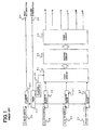
- FIG. 2 is a block diagram of the control circuit in accordance with the present invention.
- the control circuit comprises a first circuit 2 for generating a three-phase PWM signal, and a second circuit 1 for generating an analog-digital trigger.
- the first circuit 2 has three functions: the first function is to generate PWM signals necessary for a system for driving a three-phase motor by means of an invertor, that is, signals U0 and U1 for controlling upper and lower arms of a U-phase invertor, signals V0 and V1 for controlling a V-phase invertor, and signals W0 and W1 for controlling a W-phase invertor, and to output those signals to terminals; the second function is to generate the second interruption 35 at a carrier period; and the third function is to generate the first interruption 34 at an intermediate point of a carrier period.
- the second circuit 1 comprises a first compare register 11 and a second compare register 13 both always making comparison with the timer 21 to thereby transmit a coincidence signal, a first buffer register 12 and a second buffer register 14 associated with the first compare register 11 and the second compare register 13, respectively, an A/D trigger selecting circuit 15 which selects one of the coincidence signals transmitted from the first and second compare registers 11 and 13, and outputs an analog-digital start trigger signal 16, and an A/D conversion time setting register 17 which stores a value reflecting the time necessary for conducting analog-digital conversion in an analog-digital convertor equipped in a micro-computer in which the control circuit in accordance with the present invention is also equipped.
- the second circuit 1 Since the second circuit 1 outputs an analog-digital start trigger slightly before a timing at which U-phase varies, when the timer 21 is in counting-down operation, an output signal transmitted from the U-phase first buffer register 25 to which an output signal transmitted from the A/D conversion time setting register 17 is added is trallsmitted to the second buffer register 14.
- Timings at which the first and second buffer registers 12 and 14 transfer their outputs to the first and second compare registers 11 and 13, respectively, are identical with timings at which the first to third buffer registers 25, 27 and 29 transfer their outputs to the first to third compare registers 24, 26 and 28, respectively, in the first circuit 2. That is, the timings are in aynchronization with the second periodic interruptions 35 generated from the timer 21.
- Designing compare registers having such a two-staged structure as mentioned above makes it no longer necessary to consider a time necessary for dealing with data through software, because a value for a next period can be set in the previous period.
- the A/D trigger selecting circuit 15 selects a coincidence signal transmitted from the first compare register 11 when the timer 21 is in counting-up operation, whereas selects a coincidence signal transmitted from the second compare register 13 when the timer 21 is in counting-down operation.
- an up- and down-counting flag 30 holding status of the timer 21 as to whether the timer 21 is in counting-up or counting-down operation transmits its output signal to the A/D trigger selecting circuit 15.
- the second circuit 1 automatically generates the analog-digital start trigger 16 in synchronization with a timing at which a three-phase PWM signal is output.
- FIG. 3 is a circuit diagram of a circuit for controlling a three-phase motor by means of an invertor.
- feedback control In order to accurately control a three-phase motor, it would be necessary to always monitor rotation of the three-phase motor, and carry out control by which the monitored rotation is fed-back to a PWM control signal. Hereinbelow, such control is referred to as "feedback control". In order to monitor rotation of a three-phase motor, it would be necessary to detect a U-phase current Iu, a V-phase current Iv and a W-phase current Iw in the three-phase motor by means of an analog-digital convertor.
- the phase currents Iu, Iv and Iw are directly detected.
- a timing at which analog-digital conversion is carried out is identical with PWM periodic interruption, and accordingly, the second interruption 35 illustrated in FIG. 2 can be used for A/D conversion.
- each analog-digital conversion has to be carried out at a high rate.
- the second circuit 1 for generating an analog-digital trigger in the control circuit in accordance with the present invention makes it possible to carry out such analog-digital conversion.
- timing tuning has to be carried out in the second method, analog-digital conversion is carried out only once at one timing, and hence, the analog-digital conversion is not always necessary to be high-rate A/D conversion.
- control circuit in accordance with the present invention automatically generates an optimal analog-digital start trigger regardless of feedback control to be carried out in a three-phase motor. Accordingly, optimal feedback control can be accomplished in one micro-computer without an increase in dealing with data through software.
- control circuit in accordance with the present invention automatically generates an optimal analog-digital start trigger regardless of feedback control to be carried out in a three-phase motor. Accordingly, optimal feedback control can be accomplished in one micro-computer without an increase in dealing with data through software.
- each of the compare registers is designed to have a two-staged structure in the control circuit in accordance with the present invention, a value for a next period can be set in the previous period. As a result, it is no longer necessary to consider a time necessary for dealing with data through software, when data is dealt with.
- the control circuit in accordance with the first embodiment comprises a three-phase PWM signal generating circuit 2 for generating a three-phase PWM signal, and an analog-digital trigger generating circuit 1 for generating an analog-digital trigger.
- the three-phase PWM signal generating circuit 2 for generating a three-phase PWM signal comprises a timer 21, a first compare register 22, a second compare register 24, a third compare register 26, a fourth compare register 28, a first buffer register 23, a second buffer register 25, a third buffer register 27, a fourth buffer register 29, an up- and down-counting flag 30, a first circuit 31 for generating a PWM signal, a second circuit 32 for generating dead time, and a third circuit 33 for controlling an output to be transmitted from the control circuit.
- the timer 21 generates a carrier period having a PWM waveform. If a carrier wave has a triangular waveform, the timer 21 carries out counting-up and counting-down operations.
- the first compare register 22 controls a period of the timer 21.
- the first compare register 22 always makes comparison with an output transmitted from the timer 21, and converts an operation to be carried out by the timer 21 from counting-up operation to counting-down operation, if the first compare register 22 detects coincidence with the output signal transmitted from the timer 21.
- the first compare register 22 generates first interruption 34, and the timer 21 generates second interruption 35.
- the up- and down-counting flag 30 indicates a status of the timer 21. While the timer 21 is in counting-up operation, the up- and down-counting flag 30 is in a low level, whereas while the timer 21 is in counting-down operation, the up- and down-counting flag 30 is in a high level.
- the second compare register 24 generates a U-phase timing.
- the second compare register 24 always makes comparison with an output signal transmitted from the timer 21, and outputs a coincidence signal or a one shot pulse signal, if the second compare register 24 detects coincidence with the output signal.
- the third compare register 26 generates a V-phase timing.
- the third compare register 26 always makes comparison with an output signal transmitted from the timer 21, and outputs a coincidence signal or a one shot pulse signal, if the third compare register 26 detects coincidence with the output signal.
- the fourth compare register 28 generates a W-phase timing.
- the fourth compare register 28 always makes comparison with an output signal transmitted from the timer 21, and outputs a coincidence signal or a one shot pulse signal, if the fourth compare register 28 detects coincidence with the output signal.
- the coincidence signals generated by the second to fourth compare registers 24, 26 and 28 are transmitted to the firet circuit 31.
- the first circuit 31 On receipt of the coincidence signals, the first circuit 31 generates a signal based on which positive-phase and opposite-phase signals in each of the phases are generated.
- dead time means a time for preventing positive and opposite phases of an invertor from short-circuiting with each other.
- the second circuit 32 transmits its output signal to the third circuit 33, which then transmits U0, U1, V0, V1, W0 and W1 signals to terminals of a micro-computer.
- the analog-digital trigger generating circuit 1 comprises a fifth compare register 15 and a sixth compare register 13 both always making comparison with the timer 21 to thereby transmit a coincidence signal, a fifth buffer register 12 and a sixth buffer register 14 associated with the fifth compare register 11 and the sixth compare register 13, respectively, an A/D trigger selecting circuit 15 which selects one of the coincidence signals transmitted from the fifth and sixth compare registers 11 and 13, and outputs an analog-digital start trigger signal 16, and an A/D conversion time setting register 17 which stores a value reflecting the time necessary for conducting analog-digital conversion in an analog-digital convertor (not illustrated) equipped in a micro-computer in which the control circuit in accordance with the first embodiment is also equipped.
- the fifth compare register 11 is associated with the fifth buffer register 12 to thereby define a two-stages structure.
- the fifth buffer register 12 transfers its output signal to the fifth compare register 11 at the second periodic interruption 35 generated at under-flow of the timer 21, when the timer 21 operates in a symmetrical triangular wave.
- the two-staged structure defined by the fifth compare register 11 and the fifth buffer register 12 makes it no longer necessary to consider a time necessary fox dealing with data through software, because a value for a next period can be set in the previous period.
- the sixth compare register 13 and the sixth buffer register 14 are designed to have the same structures as the structures of the fifth compare register 11 and the fifth buffer register 12, respectively.
- the A/D conversion time setting register 17 stores the time necessary for carrying out analog-digital conversion (or the time necessary for sampling) in an analog-digital convertor (not illustrated) equipped in a micro-computer in which the control circuit in accordance with the first embodiment is also equipped.
- the time necessary for carrying out A/D conversion is dependent on a value designated in a register equipped in the analog-digital convertors but is generally determined in accordance with a command transmitted from a central processing unit.
- the A/D conversion time setting register 17 stores a value reflecting the above-mentioned value designated in a register equipped in the analog-digital convertor.
- Subtraction between the A/D conversion time setting register 17 and the fourth buffer register 29 is stored in the fifth buffer register 12, and addition of the A/D conversion time setting register 17 and the second buffer register 25 is stored in the sixth buffer register 14.
- the A/D trigger selecting circuit 15 automatically selects a coincidence signal transmitted from the fifth compare register 11 and a coincidence signal transmitted from the sixth compare register 13, and generates the A/D start trigger 16.
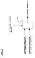
- FIG. 4 is a block diagram of an example of the A/D trigger selecting circuit 15.
- the A/D trigger selecting circuit 15 may comprise for instance, a selector 151 which receives an output signal transmitted from the up- and down-counting flag 30, a coincidence signal transmitted from the fifth compare register 11, and a coincidence signal transmitted from the sixth compare register 13.
- the up- and down-counting flag 30 constituting the three-phase PWM signal generating circuit 2 is a status-holding flag. Specifically, the up- and down-counting flag 30 is in a low level when the timer is in counting-up operation, and in a high level when the timer 21 is in counting-down operation.
- the selector 151 selects a coincidence signal transmitted from the fifth compare register 11 when the up- and down-counting flag 30 is in a low level, whereas selects a coincidence signal transmitted from the sixth compare register 13 when the up- and down-counting flag 30 is in a high level.
- the selected coincidence signal is transmitted from the A/D trigger selecting circuit 15 as the A/D start trigger 16.
- the A/D start trigger 16 is a signal on receipt of which the analog-digital convertor starts analog-digital conversion.
- the timer 21 generates a carrier period having a PWM waveform. If a carrier wave has a triangular waveform, the timer 21 carries out counting-up and counting-down operations.
- the first compare register 22 controls a period of the timer 21.
- the first compare register 22 always makes comparison with an output transmitted from the timer 21, and converts an operation to be carried out by the timer 21 from counting-up operation to counting-down operation, if the first compare register 22 detects coincidence with the output signal transmitted from the timer 21.
- the up- and down-counting flag 30 is a status-holding flag. Specifically, the up- and down-counting flag 30 is in a low level when the timer is in counting-up operation, and in a high level when the timer 21 is in counting-down operation.
- the second compare register 24 generates a U-phase timing.
- the second compare register 24 always makes comparison with an output signal transmitted from the timer 21, and outputs a coincidence signal or a one shot pulse signal, if the second compare register 24 detects coincidence with the output signal.
- the third compare register 26 generates a V-phase timing.
- the third compare register 26 always makes comparison with an output signal transmitted from the timer 21, and outputs a coincidence signal or a one shot pulse signal, if the third compare register 26 detects coincidence with the output signal.
- the fourth compare register 28 generates a W-phase timing.
- the fourth compare register 28 always makes comparison with an output signal transmitted from the timer 21, and outputs a coincidence signal or a one shot pulse signal, if the fourth compare register 28 detects coincidence with the output signal.
- the coincidence signals generated by the second to fourth compare registers 24, 26 and 28 are transmitted to the first circuit 31.
- the first circuit 31 On receipt of the coincidence signals, the first circuit 31 generates a signal based upon which positive-phase and opposite-phase signals in each of the phases are generated.
- the signal generated in the first circuit 31 is transmitted to the second circuit 32. Based on the received signal, the second circuit 32 generates a timing to which dead time is added.
- the second circuit 32 transmits its output signal to the third circuit 33, which then transmits U0, U1, V0, V1, W0 and W1 signals to terminals of a micro-computer.
- FIG. 5 is a timing chart showing an operation of the timer 21 and various timings.
- a gap in a timing between U0 and U1 signals, a gap in a timing between V0 and V1 signals, and a gap in a timing between W0 and W1 signals are all equal to a dead time width.
- the first interruption 34 is generated by virtue of coincidence between the first compare register 22 and the timer 21.
- a timing at which the first interruption 34 is generated is a summit of a triangular wave carrier.
- the second interruption 35 is generated by virtue of under-flow in the timer 21.
- a timing at which the under-flow is generated is a bottom of a triangular wave carrier.
- the timer 21 makes triangular wave operation, and coincidence timings in the first to fourth compare registers 22, 24, 26 and 28 are symmetrical about a summit of the triangular wave.
- the three-phase PWM signal generating circuit 2 operates in the above-mentioned manner.
- the circuit illustrated in Fig. 3 includes first to sixth bipolar transistors 43, 44, 45, 46, 47 and 48 electrically connected between a power source 41 and a ground (GND) 42, as invertors.
- the first bipolar transistor 43 has a collector electrically connected to the power source 41, and an emitter electrically connected to a collector of the second bipolar transistor 44.
- the second bipolar transistor 44 has a grounded emitter.
- the third bipolar transistor 45 has a collector electrically connected to the power source 41, and an emitter electrically connected to a collector of the fourth bipolar transistor 46.
- the fourth bipolar transistor 46 has a grounded emitter.
- the fifth bipolar transistor 47 has a collector electrically connected to the power source 41, and an emitter electrically connected to a collector of the sixth bipolar transistor 48.
- the sixth bipolar transistor 48 has a grounded emitter.
- the first and second bipolar transistors 43 and 44, the third and fourth bipolar transistors 45 and 46, and the fifth and sixth bipolar transistors 47 and 48 are electrically connected in parallel with one another between the power source 41 and the ground 42.
- the U0, U1, V0, V1, W0 and W1 signals transmitted from three-phase PWM signal generating circuit 2 are input into the first to sixth bipolar transistors 43, 44, 45 46, 47 and 48, respectively, through their gates.
- a current Tu running between an emitter of the first bipolar transistor 43 and a collector of the second bipolar transistor 44, a current Iv running between an emitter of the third bipolar transistor 45 and a collector of the fourth bipolar transistor 46, and a current Iw running between an emitter of the fifth bipolar transistor 47 and a collector of the sixth bipolar transistor 48 are all input into a motor 49.
- timings a1 and a2 at which the second compare register 24 and the timer 21 are coincident with each other, timings b1 and b2 at which the third compare register 26 and the timer 21 are coincident with each other, and timings c1 and c2 at which the fourth compare register 28 and the timer 21 are coincident with each other are identical with any one of turning points of the U0, U1, V0, V1, W0 and W1 terminals.
- the timing a1 is identical with a timing at which the U1 terminal falls down
- the timing a2 is identical with a timing at which the U0 terminal falls down.
- Signals at the U0, U1, V0, V1, W0 and W1 terminals are timing signals used for controlling gates of invertors in the circuit illustrated in FIG. 3.
- the invertors turn on or off, and hence, an invertor current is in a transition period and not stable in the certain period.
- a timing at which a stable inventor current can be detected is limited to either a timing slightly before the timings a1, a2, b1, b2, c1 and c2 (that is, immediately before a turning-on or turning-off period) or a timing after the turning-on or turning-off period.
- a band during which a current can be detected would be quite narrow. Accordingly, it would be preferable to select a timing slightly before the timings a1, a2, b1, b2, c1 or c2 as a timing at which a stable current is detected.
- a timing immediately before the timing b2 is identical with a timing immediately before the tuning c1. Hence, it would be possible to detect the current Iw as the current Ia,
- a timing immediately before the timing a2 is identical with a timing immediately before the timing b1. Hence, it would be possible to detect the current Iu as the current Ia.
- effective timings are a timing immediately before the timing b1, a tuning immediately before the timing c1, a timing immediately before the timing b2, and a timing immediately before the timing a2.
- the same status is detected at both a timing immediately before the b1 and a timing immediately before the timing a2, and the same status is detected at both a timing immediately before the c1 and a timing immediately before the timing b2.
- the fifth buffer register 12 transfers its output signal to the fifth compare register 11 through the second interruption 35
- the sixth buffer register 14 transfers its output signal to the sixth compare register 13 through the first interruption 34.
- the two-staged structure in the compare registers makes it no longer necessary to consider the time necessary for dealing with data through software, because a value for a next period can be set in the previous period.
- the compare registers 22, 24, 26 and 28 in the three-phase PWM signal generating circuit 2 are designed to have a two-staged structure
- the compare registers 11 and 13 in the A/D trigger generating circuit 1 are also designed to have a two-staged structure, because the compare registers 11 and 13 are necessary to operate in synchronization with the compare registers 22, 24, 26 and 28.
- timings c3 and a3 are shown in FIG. 5. Since both the timings c3 and a3 do not overlap periods in which the invertors are turned on or off, it would be possible to detect a current at a timing at which the current is in stable condition,
- the timing c3 is within the counting-up operation of the timer 21, and the tuning a3 is within the counting-down operation of the timer 21.
- the A/D trigger selecting circuit 15 having such a structure as illustrated in FIG. 4 selects a coincidence signal (timing c3) transmitted from the fifth compare register 11, as an A/D start trigger when the timer 21 is in counting-up operation, whereas selects a coincidence signal (timing a3) transmitted from the sixth compare register 13, as an A/D start trigger when the timer 21 is in counting-down operation.
- the A/D trigger generating circuit 1 makes it possible to start analog-digital conversion at a timing which is optimal to feedback control and at which a turning-on or -off period of the invertors and an A/D conversion period do not overlap each other.
- control circuit in accordance with the first embodiment provides the following advantages.
- the current Ia running through the three-phase invertor motor is detected for carrying out the feedback control.
- the A/D trigger selecting circuit 1 automatically generates an A/D trigger optimal to the feedback control.
- control circuit in accordance with the first embodiment provides advantages of reduction in the number of parts, reduction in an area of a substrate and cost reduction.
- the analog-digital trigger selecting circuit 1 in the first embodiment were arranged externally of a micro-computer, it would be necessary to load the time necessary for carrying out A/D conversion, stored in a micro-computer, to an external latching device from the micro-computer, in order to set the time in the A/D conversion time setting register 17.
- such loading a time is unnecessary from the standpoint of total system.
- control circuit in accordance with the first embodiment can solve a problem which will be caused if control is made externally of a micro-computer, ensuring enhancement in controllability.
- fifth and sixth buffer registers 12 and 14 are set through automatic calculation made between the A/D conversion time setting register 17 and the second and fourth buffer registers 25 and 29 in the three-phase PWM signal generating circuit 2, it is no longer necessary to carry out such calculation through software.
- the A/D trigger selecting circuit 15 is automatically operated by means of the selector 151, as illustrated in FIG. 4, it is not necessary to additionally carry out operation of the A/D trigger selecting circuit 15 through software.
- control circuit in accordance with the first embodiment provides the same functions provided by the conventional control circuit, without an increase in burden to software.
- timings c3 and a3 shown in the timing chart of FIG. 5 are selected as the analog-digital conversion timing in the first embodiment, a timing immediately before the timing b1 and a timing immediately before the timing b2 may be selected as the analog-digital conversion timing.
- the A/D conversion time setting register 17 is designed to store only one value corresponding to one analog-digital conversion, analog-digital conversion is carried out once on receipt of the A/D start trigger 16. If analog-digital conversion is to be repeatedly carried out a plurality of times, the A/D conversion time setting register 17 is designed to store R ⁇ T values wherein R dicates the time necessary for carrying out analog-digital conversion, and T indicates the number of repetition.
- a value reflecting the repetition number may be stored in the A/D conversion time setting register 17.
- the A/D conversion time setting register 17 may be designed to be set in accordance with commands transmitted from a central processing unit, which ensures the A/D conversion time setting register 17 can be tuned through software. To this end, the A/D conversion time setting register 17 is designed to have such a structure that a value written in accordance with commands transmitted from a central processing unit is stored, if the commands are written over an automatically set value.
- control circuit in accordance with the second embodiment is designed to include the analog-digital trigger selecting circuit having a different structure from that of the analog-digital trigger selecting circuit in the first einbodiment,
- control circuit in accordance with the second embodiment is designed to include an A/D trigger selecting circuit 15a having such a structure as illustrated in FIG. 6 in place of the A/D trigger selecting circuit 15 having the structure illustrated in FIG. 4.
- the control circuit in accordance with the second embodiment has the same structure as the structure of the control circuit in accordance with the first embodiment except including the A/D trigger selecting circuit 15a in place of the A/D trigger selecting circuit 15.
- the A/D trigger selecting circuit 15a comprises a first selector 151 which receives coincidence signals transmitted from the fifth and sixth compare registers 11 and 13, a first latching device 153 which receives command signals from an external central processing unit (CPU) 155 through a bus 155a, a second latching device 154 which receives command signals from the external central processing unit (CPU) 155 through the bus 155a, and a second selector 152 which receives both output signals transmitted from the first and second latching devices 153 and 154 and an output signal transmitted from the up- and down-counting flag 30, and transmits a selection signal indicative of one of the coincidence signals, to the first selector 151.
- a first selector 151 which receives coincidence signals transmitted from the fifth and sixth compare registers 11 and 13
- a first latching device 153 which receives command signals from an external central processing unit (CPU) 155 through a bus 155a
- a second latching device 154 which receives command signals from the external central processing unit (CPU) 155 through
- the first and second latching devices 153 and 154 are comprised of register bits capable of reading and writing data through the bus 155a in accordance with commands transmitted from the central processing unit 155.
- the A/D trigger selecting circuit 15 illustrated in FIG. 4 switches the A/D start trigger 16 in accordance with an output signal transmitted from the up- and down-counting flag 30.
- the A/D trigger selecting circuit 15a switches the A/D start trigger 16 in accordance with a value stored in the first and second latching devices 153 and 154 in line with commands transmitted from the central processing unit 155.
- the A/D trigger selecting circuit 15a in the second embodiment operates in the same manner as the A/D trigger selecting circuit 15 illustrated in FIG. 4.
- the second selector 152 selects the first latching device 153.
- the first selector 151 selects a coincidence signal transmitted from the fifth compare register 11. In contrast, if the first latching device 153 outputs a signal "1", the first selector 151 selects a coincidence signal transmitted from the sixth compare register 13.
- the A/D trigger selecting circuit 15a illustrated in FIG. 6 makes. it possible to automatically select a coincidence signal by virtue of the up- and down-counting flag 30, and further select a coincidence signal in accordance with commands transmitted from the central processing unit 155.
- analog-digital conversion is to be carried out by a common trigger over a plurality of periods
- analog-digital conversion could be readily accomplished through the use of the A/D trigger selecting circuit 15a to select a coincidence signal in accordance with commands transmitted from the central processing unit 155.
- the timing necessary for carrying out the feedback control to a three-phase invertor motor is accomplished through the use of the A/D trigger generating circuit 1 without an increase in dealing with signals through software. It is not always necessary to accomplish the above-mentioned functions by means of hardware, if a central processing unit has a high processing rate.
- FIG. 7 a control circuit in accordance with the third embodiment is illustrated in FIG. 7.
- the control circuit has to additionally carry out software processing in order to compensate for the omitted functions.
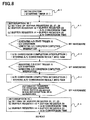
- FIG. 8 is a flow chart of additional software processing. Hereinbelow is explained additional software processing with reference to FIG. 8. In FIG. 8, only steps to be carried out for the feedback control are shown. Specifically, later mentioned steps A0 to A4 are carried out through software. The steps A1 and A4 show what is done in the second interruption 35. In the steps A1 and A4, steps (b) and (c) among the steps (a), (b) and (c) have to be additionally carried out as a result of removal of hardware.
- initialization is made. That is, the timer 21 is caused to start, in step A0.
- step A1 the second interruption 35 is carried out, in step A1, as follows.
- the second to fourth buffer registers 25, 27 and 29 are set up, based on the result of A/D conversion having been caxried out in the previous period, in step A1-(a).
- a difference between the fourth buffer register 29 and a time necessary for carrying out analog-digital conversion is stored in the fifth buffer register 12, in step A1-(b).
- a difference between the second buffer register 25 and the time necessary for carrying out analog-digital conversion is stored in the sixth buffer register 14, in step A1-(c).
- a value to be stored in the fourth buffer register 29 is necessary for carrying out PWM output control, and is calculated based on the previous period in step A1-(a), and hence, the value is not generated additionally in the second embodiment.
- the time necessary for carrying out analog-digital conversion is determined in dependence on an analog-digital convertor. In general, the time necessary for carrying out analog-digital conversion is not rewritten so frequently, and the time determined in the initialization is used without being changed. Thus, once the time necessary for carrying out analog-digital conversion has been determined, the time is not necessary to change.
- step A1 since one subtraction and one addition are conducted in step A1, a load in software processing would be lightened, if a central processing unit having high calculation ability is used.
- a load in software processing is dependent on an object which is to be dealt with by a micro-computer. Hence, a load in software processing may be high, if a micro-computer has to control many objects other than a three-phase motor.
- the A/D conversion trigger selecting circuit 15 When the fifth compare register 11 coincides with an output signal transmitted from the timer 21, the A/D conversion trigger selecting circuit 15 generates the AID start trigger 16. On receipt of the A/D start trigger 16, an analog-digital convertor starts A/D conversion.
- the A/D conversion mentioned above is carried out in hardware.
- step A2 a result of the A/D conversion is stored in a memory such as RAM, in step A2.
- the A/D conversion trigger selecting circuit 15 When the sixth compare register 13 coincides with an output signal transmitted from the timer 21, the A/D conversion trigger selecting circuit 15 generates the A/D start trigger 16. On receipt of the A/D start trigger 16, an analog-digital convertor starts A/D conversion.
- the A/D conversion mentioned above is carried out in hardware.
- step A3 a result of the A/D conversion is stored in a memory such as RAM, in step A3.
- the second interruption 35 is generated, and automatic transfer is made to the fifth and sixth compare registers 11 and 13 from the fifth and sixth buffer registers 12 and 14, respectively.
- the automatic transfer is made by means of hardware.
- steps A1 to A3 are repeatedly carried out.
- the control circuit in accordance with the third embodiment makes it possible to omit automatic addition, automatic subtraction, and the A/D conversion time setting register 17 or 17a storing the time necessary for carrying out analog-digital conversion, ensuring reduction in a chip size and further in chip costs.
- the control circuit in accordance with the fourth embodiment illustrated in Fig. 9 additionally includes a preliminary circuit 4 in comparison with the control circuit in accordance with the first embodiment.
- the preliminary circuit 4 is comprised of an analog-digital conversion status flag 41 indicating whether analog-digital conversion is being carried out, a detection circuit 42 which transmits a detection signal 42a, if the detection circuit 42 detects that at least one of terminals receiving PWM signals varies in status, and an error flag setting circuit 43 which sets an error flag when the detection signal 42a is received while the analog-digital conversion status flag 41 indicates that analog-digital conversion is being carried out.
- the analog-digital conversion status flag 41 shows "1" while analog-digital conversion is being carried out, or "0" while analog-digital conversion is not being carried out.
- the functions of the analog-digital conversion status flag 41 are functions which an ordinary A/D convertor has.
- the analog-digital conversion status flag 41 in the fourth embodiment is a copy of a flag which an analog-digital convertor has.
- the detection circuit 42 transmits a one-shot pulse as the detection signal 42a, when at least one of the terminals U0, U1, V0, V1, W0 and W1 varies in status.
- the error flag setting circuit 43 sets a flag which shows "1" when the detection circuit 42 outputs the detection signal 42a while the analog-digital conversion status flag 41 shows “1", and stores a value of "1". In other words, the error flag setting circuit 43 sets an error flag when the three-phase PWM output terminal varies during analog-digital conversion.
- the timings c3 and a3 generally do not overlap a timing at which a three-phase PWM output signal is transmitted. However, for instance, while de-bagged or in abnormal operation, the timing c3 and variation in the terminal V0 or the timing a3 and variation in the terminal V1 may overlap each other. If analog-digital conversion is carried out under such circumstance, a current in transition period in which an invertor is turned on or off is converted to a digital form from an analog form, resulting in that the feedback control cannot be accurately carried out.
- the preliminary circuit 4 has a function of detecting such abnormal condition. Specifically, the preliminary circuit 4 detects abnormal condition by reading an error flag set by the error flag setting circuit 43, during analog-digital conversion completion interruption.
- the error flag setting circuit 43 in the fifth embodiment illustrated in Fig. 10 has a different function from the functions of the error flag setting circuit 43 in the fourth embodiment.
- the error flag setting circuit 43 in the fifth embodiment is designed to generate error interruption 44.
- the error interruption 44 is transmitted when the error flag 43 is set.
- the error flag setting circuit 43 which transmits the error interruption 44 presents an advantage that it is possible to transmit the error interruption 44 to inform an error immediately when it occurs, without waiting for completion of analog-digital conversion. Thus, defectiveness can be timely removed.
Landscapes
- Engineering & Computer Science (AREA)
- Power Engineering (AREA)
- Inverter Devices (AREA)
- Control Of Ac Motors In General (AREA)
- Control Of Electric Motors In General (AREA)
Abstract
Description
Claims (12)
- A control circuit including:characterized bya first circuit (2) for generating a three-phase PWM (pulse width modulation) signal, the circuit having functions of generating a PWM signal necessary for driving a three-phase invertor motor, generating interruption at a carrier period, and generating interruption at an intermediate point of a carrier period,
a second circuit (1) for generating an analog-digital start trigger (16) in synchronization with a timing at which the PWM signal is output. - The control circuit as set forth in claim 1, wherein the second circuit (1) includes a first compare register (11) having a two-staged structure, and a second compare register (13) having a two-staged structure, and the first circuit (2) includes a PWM timer (21),
the first and second compare registers (11, 13) making comparison with an output signal transmitted from the PWM timer (21) to thereby generate the analog-digital start trigger (16). - The control circuit as set forth in claim 2, wherein the first and second compare registers (11, 13) are automatically set up by automatic calculation of a timing at which the PWM signal is output.
- The control circuit as set forth in claim 1, wherein the first circuit includes a PWM timer (21), and the second circuit (1) generates two analog-digital start triggers (16), one of which is selected in synchronization with counting-up or counting-down operation of the PWM timer (21).
- The control circuit as set forth in claim 1, wherein the first circuit includes a PWM timer (21), and the second circuit (1) comprises :(b1) first and second compare registers (11, 13) each of which makes comparison with an output signal transmitted from the PWM timer (21), and outputs a coincidence signal,(b2) first and second buffer registers (12 14) associated with the first and second compare registers (11, 13), respectively, and(b3) a third circuit (15) which selects one of coincidence signals transmitted from the first and second compare registers (11, 13), to thereby generate an analog-digital start trigger signal (16).
- The control circuit as set forth in claim 5, further including a register (17) which stores a value reflecting a time necessary for carrying out analog-digital conversion an analog-digital convertor equipped in a computer in which the control circuit is equipped.
- The control circuit as set forth in claim 5, wherein the second circuit (1) further includes a selector (151) which selects one of coincidence signals transmitted from the first and second compare registers (11, 13) when the PWM timer (21) is in counting-up operation, and selects the other, when the PWM timer (21) is in counting-down operation.
- The control circuit as set forth in claim 7, wherein the first circuit (2) further includes a flag (30) which indicates whether the PWM timer (21) is in counting-up or counting-down operation, and transmits its output signal to the selector (151).
- The control circuit as set forth in claim 5, wherein transfer to the first compare register (11) from the first buffer register (12) is carried out by interruption generated at under-flow in the PWM timer (21), if the PWM timer (21) operates in a symmetrical triangle wave.
- The control circuit as set forth in claim 5, wherein the first circuit (2) further includes a flag (30) which indicates whether the PWM timer (21) is in counting-up or counting-down operation, and the third circuit (15) comprises:(b1) a first selector (151) which receives coincidence signals transmitted from the first and second compare registers (11, 13),(b2) a first latch device (153) which receives a command transmitted from an external central processing unit (155),(b3) a second latch device (154) which receives a command transmitted from an external central processing unit (155), and(b4) a second selector (152) which receives both output signals transmitted from the first and. second latch devices (153, 154) and an output signal transmitted from the flag (30), and transmits a selection signal to the first selector (151) to indicate which one of the coincidence signals is to be selected.
- The control circuit as set forth in any one of claims 1 to 10, further including an auxiliary circuit (4) including:(a) a status flag (41) which indicates whether analog-digital conversion is being carried out,(b) a detecting circuit (42) which transmits a detection signal (42a), when at least one of terminals which receive the PWM signal varies with respect to its status, and(c) an error flag setting circuit (43) which sets an error flag when the detection signal (42a) is transmitted, while the status flag (41) indicates analog-digital conversion is being carried out.
- The control circuit as set forth in claim 11, wherein the error flag setting circuit (43) generates interruption (44) when the error flag has been set.
Applications Claiming Priority (2)
| Application Number | Priority Date | Filing Date | Title |
|---|---|---|---|
| JP2001097409A JP3548540B2 (en) | 2001-03-29 | 2001-03-29 | Trigger generation circuit |
| JP2001097409 | 2001-03-29 |
Publications (2)
| Publication Number | Publication Date |
|---|---|
| EP1251632A2 true EP1251632A2 (en) | 2002-10-23 |
| EP1251632A3 EP1251632A3 (en) | 2004-01-14 |
Family
ID=18951194
Family Applications (1)
| Application Number | Title | Priority Date | Filing Date |
|---|---|---|---|
| EP02090126A Withdrawn EP1251632A3 (en) | 2001-03-29 | 2002-03-28 | Circuit for generating three-phase PWM signal |
Country Status (3)
| Country | Link |
|---|---|
| US (1) | US6667598B2 (en) |
| EP (1) | EP1251632A3 (en) |
| JP (1) | JP3548540B2 (en) |
Cited By (1)
| Publication number | Priority date | Publication date | Assignee | Title |
|---|---|---|---|---|
| WO2019061186A1 (en) * | 2017-09-28 | 2019-04-04 | 华为技术有限公司 | PWM control signal synchronization method of inverter and inverter and power grid system |
Families Citing this family (14)
| Publication number | Priority date | Publication date | Assignee | Title |
|---|---|---|---|---|
| JP4665360B2 (en) * | 2001-08-06 | 2011-04-06 | 株式会社安川電機 | Electric motor control device |
| JP3993502B2 (en) * | 2002-10-21 | 2007-10-17 | 株式会社ルネサステクノロジ | Multi-phase DC motor rotation drive control device and start-up method |
| JP4509535B2 (en) * | 2002-11-19 | 2010-07-21 | パナソニック株式会社 | Semiconductor device and control method |
| US7049778B2 (en) * | 2004-02-09 | 2006-05-23 | Nippon Yusoki Co., Ltd. | Inverter control apparatus and inverter control method |
| JP4581574B2 (en) * | 2004-09-08 | 2010-11-17 | 株式会社ジェイテクト | Motor control device and electric power steering device |
| US7034478B2 (en) * | 2004-09-30 | 2006-04-25 | Agere Systems Inc. | Digital spindle control architecture |
| US7012396B1 (en) | 2004-09-30 | 2006-03-14 | Agere Systems Inc. | Increased digital spindle motor control resolution through dither |
| JP4926482B2 (en) * | 2006-01-27 | 2012-05-09 | 東芝キヤリア株式会社 | Power converter |
| JP5252475B2 (en) * | 2007-11-06 | 2013-07-31 | オムロンオートモーティブエレクトロニクス株式会社 | Control device for multiphase motor |
| JP2010074902A (en) * | 2008-09-17 | 2010-04-02 | Ricoh Co Ltd | Control method of motor drive unit |
| US8853985B2 (en) * | 2010-09-17 | 2014-10-07 | Marvell World Trade Ltd. | Back-EMF detection for motor control |
| US10591892B2 (en) * | 2015-06-05 | 2020-03-17 | Renesas Electronics America Inc. | Configurable mapping of timer channels to protection groups |
| CN109162954B (en) * | 2018-11-06 | 2020-04-03 | 迈普通信技术股份有限公司 | Fan control device |
| TWI886759B (en) * | 2024-01-19 | 2025-06-11 | 茂達電子股份有限公司 | Motor driver improving resonance noise caused by motor |
Family Cites Families (14)
| Publication number | Priority date | Publication date | Assignee | Title |
|---|---|---|---|---|
| JPH04172995A (en) * | 1990-11-02 | 1992-06-19 | Fuji Electric Co Ltd | Regulation of detecting timing for output current of inverter |
| JP3156269B2 (en) * | 1991-04-10 | 2001-04-16 | 松下電器産業株式会社 | Digital three-phase PWM waveform generator |
| JP2885256B2 (en) | 1991-12-25 | 1999-04-19 | 日本電気株式会社 | Microcomputer |
| JP3188097B2 (en) | 1994-05-10 | 2001-07-16 | オークマ株式会社 | Inverter control device |
| JP3367260B2 (en) | 1995-03-24 | 2003-01-14 | 三菱電機株式会社 | Encoder device and servo motor control device |
| JPH08317685A (en) | 1995-05-17 | 1996-11-29 | Matsushita Electric Ind Co Ltd | Inverter device |
| JPH0947065A (en) | 1995-07-25 | 1997-02-14 | Nissan Motor Co Ltd | Motor drive controller |
| JPH09121558A (en) * | 1995-10-27 | 1997-05-06 | Nissan Motor Co Ltd | Motor drive control device |
| US6026126A (en) * | 1997-04-08 | 2000-02-15 | Motorola, Inc. | Method and apparatus for reducing a ripple signal in an output of a direct current power supply |
| JP3346223B2 (en) * | 1997-06-10 | 2002-11-18 | 株式会社日立製作所 | Motor control method and motor control system |
| JPH11122938A (en) | 1997-07-29 | 1999-04-30 | Hitachi Ltd | PWM pulse generation circuit and control system using the same |
| JP2000092851A (en) * | 1998-09-14 | 2000-03-31 | Toyota Motor Corp | PWM type rotating machine controller |
| JP2000184730A (en) | 1998-12-11 | 2000-06-30 | Moriyama Kogyo Kk | Load current detection device for PWM inverter |
| JP4465129B2 (en) * | 2000-07-14 | 2010-05-19 | パナソニック株式会社 | Brushless motor driving apparatus and driving method |
-
2001
- 2001-03-29 JP JP2001097409A patent/JP3548540B2/en not_active Expired - Fee Related
-
2002
- 2002-03-28 EP EP02090126A patent/EP1251632A3/en not_active Withdrawn
- 2002-03-28 US US10/109,250 patent/US6667598B2/en not_active Expired - Lifetime
Cited By (4)
| Publication number | Priority date | Publication date | Assignee | Title |
|---|---|---|---|---|
| WO2019061186A1 (en) * | 2017-09-28 | 2019-04-04 | 华为技术有限公司 | PWM control signal synchronization method of inverter and inverter and power grid system |
| CN110462963A (en) * | 2017-09-28 | 2019-11-15 | 华为技术有限公司 | A PWM control signal synchronization method for inverter and inverter and grid system |
| US11223205B2 (en) | 2017-09-28 | 2022-01-11 | Huawei Technologies Co., Ltd. | Method for synchronizing PWM control signals of inverters, inverter, and power grid system |
| CN110462963B (en) * | 2017-09-28 | 2022-02-25 | 华为技术有限公司 | A PWM control signal synchronization method of inverter and inverter and grid system |
Also Published As
| Publication number | Publication date |
|---|---|
| JP3548540B2 (en) | 2004-07-28 |
| EP1251632A3 (en) | 2004-01-14 |
| US20020143425A1 (en) | 2002-10-03 |
| JP2002300783A (en) | 2002-10-11 |
| US6667598B2 (en) | 2003-12-23 |
Similar Documents
| Publication | Publication Date | Title |
|---|---|---|
| EP1251632A2 (en) | Circuit for generating three-phase PWM signal | |
| JP4545863B2 (en) | Semiconductor memory device | |
| JP3998624B2 (en) | Pulse width modulation waveform generation method and apparatus | |
| US5550451A (en) | Microcomputer with built-in motor control circuit | |
| JPH11339499A (en) | Parallel bit test circuit sharing output driver, parallel bit test method using the same, and semiconductor memory device thereof | |
| US6448827B1 (en) | Three-phase pulse width modulation waveform generator | |
| US5543794A (en) | Successive approximation analog-to-digital converter using CMOS inverter with pull-up and/or pull-down switches | |
| US8294487B2 (en) | Configuration setting device of integrated circuit and the configuration setting method thereof | |
| US5404116A (en) | Circuit for generating pulse width modulation signal | |
| US5175482A (en) | Stepping motor control circuit | |
| JP2818986B2 (en) | Microcomputer with built-in motor control circuit | |
| JPH0389868A (en) | Dead time compensator for inverter | |
| JP2715656B2 (en) | Analog-to-digital converter | |
| JP2555628B2 (en) | Data transfer circuit | |
| JP2944012B2 (en) | Output circuit | |
| JP3116706B2 (en) | Trigger input circuit | |
| JP2869248B2 (en) | A / D converter | |
| JP3622703B2 (en) | Pulse train generation method and apparatus, and motor rotation speed command generation apparatus using the same | |
| JPH1175375A (en) | Three-phase pulse width modulation waveform generator | |
| JPH07182267A (en) | Output control circuit | |
| JP3298908B2 (en) | Analog-to-digital converter | |
| JPH0773212B2 (en) | A / D converter | |
| JP2002100990A (en) | Programmable controller and analog input / output module | |
| KR101500778B1 (en) | Pulse signal generating apparatus for determining positions in Programmable Logic Controller | |
| JP2571007B2 (en) | Bipolar signal switch |
Legal Events
| Date | Code | Title | Description |
|---|---|---|---|
| PUAI | Public reference made under article 153(3) epc to a published international application that has entered the european phase |
Free format text: ORIGINAL CODE: 0009012 |
|
| AK | Designated contracting states |
Kind code of ref document: A2 Designated state(s): AT BE CH CY DE DK ES FI FR GB GR IE IT LI LU MC NL PT SE TR |
|
| AX | Request for extension of the european patent |
Free format text: AL;LT;LV;MK;RO;SI |
|
| RAP1 | Party data changed (applicant data changed or rights of an application transferred) |
Owner name: NEC ELECTRONICS CORPORATION |
|
| PUAL | Search report despatched |
Free format text: ORIGINAL CODE: 0009013 |
|
| AK | Designated contracting states |
Kind code of ref document: A3 Designated state(s): AT BE CH CY DE DK ES FI FR GB GR IE IT LI LU MC NL PT SE TR |
|
| AX | Request for extension of the european patent |
Extension state: AL LT LV MK RO SI |
|
| RIC1 | Information provided on ipc code assigned before grant |
Ipc: 7H 02P 7/06 B Ipc: 7H 02P 7/00 B Ipc: 7H 02M 7/5387 A |
|
| 17P | Request for examination filed |
Effective date: 20040202 |
|
| 17Q | First examination report despatched |
Effective date: 20040618 |
|
| AKX | Designation fees paid |
Designated state(s): DE GB |
|
| GRAP | Despatch of communication of intention to grant a patent |
Free format text: ORIGINAL CODE: EPIDOSNIGR1 |
|
| STAA | Information on the status of an ep patent application or granted ep patent |
Free format text: STATUS: THE APPLICATION IS DEEMED TO BE WITHDRAWN |
|
| 18D | Application deemed to be withdrawn |
Effective date: 20050722 |