EP1251546A2 - Electronic device sealed under vacuum containing a getter and method of operation - Google Patents
Electronic device sealed under vacuum containing a getter and method of operation Download PDFInfo
- Publication number
- EP1251546A2 EP1251546A2 EP02252480A EP02252480A EP1251546A2 EP 1251546 A2 EP1251546 A2 EP 1251546A2 EP 02252480 A EP02252480 A EP 02252480A EP 02252480 A EP02252480 A EP 02252480A EP 1251546 A2 EP1251546 A2 EP 1251546A2
- Authority
- EP
- European Patent Office
- Prior art keywords
- electronic device
- substrate
- temperature
- evaporable getter
- getter material
- Prior art date
- Legal status (The legal status is an assumption and is not a legal conclusion. Google has not performed a legal analysis and makes no representation as to the accuracy of the status listed.)
- Withdrawn
Links
Images




Classifications
-
- B—PERFORMING OPERATIONS; TRANSPORTING
- B81—MICROSTRUCTURAL TECHNOLOGY
- B81B—MICROSTRUCTURAL DEVICES OR SYSTEMS, e.g. MICROMECHANICAL DEVICES
- B81B7/00—Microstructural systems ; Auxiliary parts of microstructural devices or systems
- B81B7/0032—Packages or encapsulation
- B81B7/0035—Packages or encapsulation for maintaining a controlled atmosphere inside of the chamber containing the MEMS
- B81B7/0038—Packages or encapsulation for maintaining a controlled atmosphere inside of the chamber containing the MEMS using materials for controlling the level of pressure, contaminants or moisture inside of the package, e.g. getters
-
- H—ELECTRICITY
- H01—ELECTRIC ELEMENTS
- H01J—ELECTRIC DISCHARGE TUBES OR DISCHARGE LAMPS
- H01J29/00—Details of cathode-ray tubes or of electron-beam tubes of the types covered by group H01J31/00
- H01J29/94—Selection of substances for gas fillings; Means for obtaining or maintaining the desired pressure within the tube, e.g. by gettering
-
- H—ELECTRICITY
- H10—SEMICONDUCTOR DEVICES; ELECTRIC SOLID-STATE DEVICES NOT OTHERWISE PROVIDED FOR
- H10W—GENERIC PACKAGES, INTERCONNECTIONS, CONNECTORS OR OTHER CONSTRUCTIONAL DETAILS OF DEVICES COVERED BY CLASS H10
- H10W76/00—Containers; Fillings or auxiliary members therefor; Seals
- H10W76/40—Fillings or auxiliary members in containers, e.g. centering rings
- H10W76/42—Fillings
- H10W76/48—Fillings including materials for absorbing or reacting with moisture or other undesired substances
-
- H—ELECTRICITY
- H01—ELECTRIC ELEMENTS
- H01J—ELECTRIC DISCHARGE TUBES OR DISCHARGE LAMPS
- H01J2329/00—Electron emission display panels, e.g. field emission display panels
Definitions
- This invention relates generally to electronic devices that incorporate a vacuum packaged microelectronic device. More particularly, the present invention relates to an electronic device having a non-evaporable getter material disposed on the same substrate as the active transistors and other logic devices.
- FEDs field emission displays
- MEMS micro-electro-mechanical systems
- ARS atomic resolution storage devices
- connections to or a means of activating the getter material once it is sealed within the vacuum package is also required. Further a path of sufficient cross sectional area to allow for the gaseous material outgassing from various surfaces of the device to impinge upon the surface of the getter material is necessary for efficient pumping action.
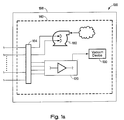
- Fig. 1a is a block diagram of an electronic device sealed under a vacuum according to a first embodiment of this invention
- Fig. 1b is a block diagram of an electronic device sealed under a vacuum according to a second embodiment of this invention.
- Fig. 3 is a cross-sectional view of an electronic device sealed under a vacuum according to an alternate embodiment of this invention
- Fig. 4 is a cross-sectional view of an electronic device sealed under a vacuum according to an alternate embodiment of this invention.
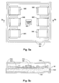
- Fig. 5a is a schematic view of an electronic device sealed under a vacuum according to an alternate embodiment of this invention.
- Fig. 5b is a cross-sectional view of an electronic device sealed under a vacuum according to an alternate embodiment of this invention.
- Fig. 6 is a flow diagram of a method for activating the NEG material according to an embodiment of this invention.
- Fig. 7 is a flow diagram of a method for reactivating the NEG material according to an alternate embodiment of this invention.
- Fig. 8 is a flow diagram of a method for reactivating the NEG material according to an embodiment of this invention.
- Fig. 1a is a block diagram of an electronic device sealed and maintained under vacuum, according to an embodiment of this invention.
- This device is referred to as electronic device 100 utilizing non-evaporable getter pump 180 (hereinafter NEG pump 180) to assist in evacuation, sealing, and maintenance of the vacuum during operation.
- NEG pump 180 non-evaporable getter pump 180
- Electronic device 100 includes the integration of NEG pump 180, vacuum device 130, and transistors 120 onto substrate 140 enclosed in package 196 that is vacuum-sealed.
- Vacuum device 130 relates to any electronic device that requires a vacuum to operate such as a charged particle emitter (e.g. electron or ion). Bond pads 164 are also affixed to substrate 140 providing electrical input and output.
- a charged particle emitter e.g. electron or ion
- NEG pump 180 includes non-evaporable getter material 18 1 (hereinafter NEG material 18 1) as shown in Fig. 2.
- An important aspect of the present invention is the deposition of the non-evaporable getter material directly onto the substrate utilized for both vacuum device 130 and transistors 120. This provides a reduction in the size of package 196 as well as the elimination of a separate getter cartridge that is utilized conventionally.
- another important aspect is the ability to directly heat NEG material 18 1 (see Fig. 2) to its activation temperature of between 400°C - 900" C without damaging transistors 120 or vacuum device 130.
- electronic device 10 1 includes temperature sensor 104, and pressure sensor 106, to measure the temperature of substrate 140 and the pressure within package 196 respectively.
- pressure sensor 106 senses a pressure within package 196 greater than a predetermined pressure NEG pump 180 is activated.
- temperature sensor 104 senses a substrate temperature greater than a predetermined temperature electrical power pulses to NEG pump 180 will be stopped, adding further protection to transistors 120 and vacuum device 130.
- electronic device 105 includes temperature sensor 104, pressure sensor 106, pump driver 12 1, and pulse generator 102 are all integrated with vacuum device 130, NEG pump 180 and transistors 120 on substrate 140.
- Temperature sensor 104 measures the temperature of substrate 140 and pressure sensor 106 measures the pressure within package 196.
- temperature sensor 104 and pressure sensor 106 are used to gate the electrical power pulses generated by pulse generator 102.
- pulse generator 102 will send a signal to pump driver 12 1 to apply electrical power pulses to NEG pump 180.
- the predetermined pressure is in the range of 10 -2 to 10 -5 torr and is preferably greater than 10 -3 torr.
- temperature sensor 104 senses a substrate temperature greater than a predetermined temperature pulse generator 102 will not apply electrical power pulses to NEG pump 180.
- the predetermined temperature is in the range of 300" C to 500°C and is preferably 400°C or greater.
- pressure sensor 106 determines when to activate NEG material 181 (see Fig. 2) and temperature sensor 104 protects transistors 120 and vacuum device 130 from damage while heating NEG material 18 1 to its activation temperature between 400" C - 900" C.
- This embodiment further provides an ability to increase the gettering action of NEG pump 180 while providing protection of transistors 120 and vacuum device 130.
- Fig. 2 schematically illustrates in a cross-sectional view the construction of an embodiment of electronic device 200 of the present invention having integrated NEG pump 180, vacuum device 130, and transistors 120.
- substrate 140 is preferably manufactured using a silicon wafer having a thickness of about 600-800 microns.
- transistors 120 as well as other logic devices required for electronic device 100 are formed in substrate 140.
- Transistors 120 are represented as only a single layer in Figs. 2-5 to simplify the drawing. Those skilled in the art will appreciate that transistors 120 can be realized as a stack of thin film layers. The particular structure of transistors 120 is not relevant to the invention, however some type of solid state electronic device is preferably present, such as, metal oxide field effect transistors (MOSFET), bipolar junction transistors (BJT), or other temperature sensitive device. Transistors 120 are exemplary of any semiconductor device whose operation is degraded by high temperatures such as greater than 400" C. Normally there is a passivation layer on the surface of NEG material 18 1 when exposed to ambient conditions.
- MOSFET metal oxide field effect transistors
- BJT bipolar junction transistors
- Dielectric layer 150 is disposed over transistors 120 as well as other logic devices on substrate 140. Dielectric layer 150 provides thermal insulation protecting transistors 120 as well as other logic devices from high temperature during operation of NEG pump 180.
- dielectric layer 150 is silicon oxide (Si x O y ), however, those skilled in the art will appreciate that other dielectric materials such as silicon nitride, silicon carbide, aluminum oxide, boron nitride and other low thermal conductivity materials as well as various combinations thereof can be utilized.
- dielectric layer 150 can include a first dielectric layer of silicon oxide (Si x O y ) disposed over transistors 120 with a second dielectric layer of silicon nitride (Si x N y ) disposed over the silicon oxide layer and a third dielectric layer of silicon carbide disposed over the silicon nitride layer.
- Conductive layer 160 is disposed over dielectric layer 150 and electrically couples to electrical contact regions 124 of transistors 120 through via openings 158 formed in dielectric layer 150.
- Vacuum device 130 is disposed over a portion of dielectric layer 150.
- vacuum device 130 is an electron emitter device commonly referred to as a Spindt tip or flat emitter.
- vacuum device 130 can also be a digital mirror device, digital micro mover as well as other devices utilized in field emission displays, atomic resolution storage systems and micro-electro-mechanical systems (MEMS) that are incorporated within a vacuum package.
- MEMS micro-electro-mechanical systems
- Conductive layer 160 routes signals from transistors 120 as well as other logic devices to vacuum device 130 and from bond pads 164 to NEG pump 180 as well as vacuum device 130.
- conductive layer 160 makes an electrical connection between the bond pads 164 and first and second overlapping areas 163 and 165.
- conductive layer 160 may consist of aluminum, copper, or gold, with aluminum being preferred.
- the metals used to form conductive layer 160 may be doped or combined with other materials, including copper and/or silicon.
- conductive layer 160 will have a uniform thickness of about 2000 - 7000 angstroms (about 5000 angstroms is preferable), and is applied using conventional sputtering or vapor deposition techniques.
- NEG material 18 1 is disposed over a portion of dielectric layer 150 through conductor opening 162.
- First and second overlapping areas 163 and 165 between conductive layer 160 and NEG material 18 1 are chosen to minimize the heat loss of NEG material 18 1 when heated and to minimize the electrical resistance of the electrical contact between NEG material 18 1 and conductive layer 160.
- the thickness and resistivity of NEG material 18 1 together with the two-dimensional pattern between first and second overlapping areas 163 and 165 determines the resistance of NEG material 18 1.
- the power applied to NEG material 18 1 determines the rate of temperature increase.
- the area and volume of NEG material 18 1 determines the getter capacity of NEG pump 180. Getter materials include titanium, zirconium, thorium, and molydenum.
- the getter material is a zirconium-based alloy such as Zr-Al, Zr-V, or Zr-V-Fe alloys.
- NEG material 18 1 is preferably applied using conventional sputtering or vapor deposition techniques. However, those skilled in the art will appreciate that electrophoresis, manual, or mechanical application, such as sprays or suspensions of the getter material in a suspending medium, can also be utilized. In general, NEG material 18 1 will have a uniform thickness between 0.1150 microns about 1 micron is preferable.
- a significant advantage of the present invention as shown in Fig. 2 is that a single substrate such as silicon can be used for the fabrication of MOSFET or bipolar driver transistors in and for the fabrication of non-evaporable getter pumps. These various devices may then be interconnected using standard multi-level metal interconnect technology that is well known in the art of semiconductor manufacturing.
- vacuum seal 192 is disposed on substrate 140 and cover 190 is affixed to vacuum seal 192 such that interspace region 194 is maintained at a pressure of less than 10" torr.
- the vacuum is maintained at a pressure of less than 10 -5 ton-.
- the seal can be made by a variety of techniques including thermal compression, brazing, anodic bonding, as well as other techniques.
- Fig. 3 schematically illustrates the construction of an alternate embodiment of the present invention, showing electronic device 300 utilizing electrically resistive layer 270 to provide the heating mechanism for NEG material 181.
- substrate 140, transistors 120, dielectric layer 150, and vacuum device 130 are substantially the same as shown in Fig. 2.
- Electrically resistive layer 270 is disposed over dielectric layer 150 and electrically couples to electrical contact regions 124 of transistors 120 through via openings 158 formed in dielectric layer 150.
- electrically resistive layer 270 forms heater 242 to activate NEG material 18 1 in NEG pump 180.
- Vacuum device 130 is disposed over a portion of substrate 140.
- Conductive layer 260 is disposed over electrically resistive layer 270.
- conductive layer 260 and electrically resistive layer 270 route signals from transistors 120 as well as other logic devices to vacuum device 130 and from bond pads 264 to both NEG pump 180 and vacuum device 130.
- NEG material 18 1 is disposed on a portion of resistive layer 270 within conductor opening 262.
- the thickness and resistivity of electrically resistive layer 270 together with the two-dimensional pattern of electrically resistive layer 270 underneath NEG material 18 1 determines the resistance of heater 242.
- the power applied to heater 242 determines the rate of temperature increase of NEG material 18 1.
- the addition of heater 242 in this embodiment has the primary advantage that it enables the use of getter materials, which have a high resistivity.
- Fig. 5a schematically illustrates a layout of an alternate embodiment of the present invention with cover 590 removed (see Fig. 5b), showing multiple NEG pumps 580 disposed around the periphery of electronic device 500.
- the advantage of this embodiment is the ability to utilize regions of substrate 540 which would not be as fully utilized by active devices because of the potential for damage during the singulation process when forming discreet devices from the silicon wafer.
- the constructions of the NEG pump, the transistors, and the vacuum device shown in alternate embodiments in Figs. 2-4 can all be utilized.
- Fig. 5b shows substrate 540 disposed within cover 590, base 591, and vacuum seal 192.
- Substrate 540 is mounted to base 591 forming interspace 594 between cover 590 and vacuum device 130.
- NEG material 581 is also shown in Fig. 5b as well as vacuum device 130.
- Fig. 6 shows a flow diagram of a method for activating NEG pump 180 as depicted in Fig. 1a-1d.
- electronic device 100 is placed in a vacuum chamber at a temperature less than 80" C and the device is evacuated to a pressure of less than 0.1 torr.
- thermal energy is being utilized the temperature of the chamber is increased to a temperature preferably greater than 100" C.
- photons in particular photons in the ultraviolet region of the spectrum
- electrons or ions or other charged particles can also be utilized.
- Step 614 consists of monitoring the pressure of interspace region 194.
- the pressure is compared to a pre-selected value X, if the pressure is less than the pre-selected value X then the process moves to step 618.
- the pre-selected value X for the pressure in the interspace region is less than lx 10 -5 torr, however, pressures less than 1 x 10 -3 torr are sufficient for many purposes.
- electrical power pulses are applied to NEG material 18 1 to heat NEG material 181 to its activation temperature. Getter activation occurs when the passivation layer on the surface of NEG material 18 1 diffuses into the bulk of the material.
- step 6 18 is repeated and additional electrical power pulses are applied to NEG material 181. This sequence of steps (steps 618 - 620) is repeated until the desired pressure is obtained.
- the value of the desired pressure is dependent on the pre-selected value at which activation is started as well as the amount of NEG material 181 present on substrate 140 of electronic device 100.
- step 622 is performed resulting in the sealing of electronic device 100.
- the sealing of electronic device 100 e.g. step 622
- step 616 can also be performed after step 6 16 with subsequent activation of NEG material 18 1 occurring after the sealing has been completed.
- step 620 monitoring the pressure Y cannot be carried out.
- NEG pump 180 may be advantageous to reactivate NEG pump 180 from time to time during its normal operation to maintain the desired pressure in interspace region 194 (see Fig. 2).
- the non-evaporable getter material is reactivated by applying sufficient electrical power pulses to NEG material 18 1 after a predetermined time.
- Fig. 7 shows a flow diagram of a method for reactivating NEG pump 180 as shown in Figs. 1 b-1d that uses a subroutine labeled reactivation.
- Step 7 16 consists of determining the pressure Pi of interspace region 194.
- the pressure is compared to reference pressure P 1, if the pressure is less than the reference pressure P1 then the subroutine is exited.
- step 722 will be performed and substrate temperature Ts will be determined.
- step 724 the substrate temperature is compared to reference temperature T1, if substrate temperature Ts is less than or equal to reference temperature T1 then step 726 is performed and electrical power pulses are applied to NEG material 181 to heat NEG material 181 to its activation temperature. After step 726 is completed the subroutine returns to step 716. However, if substrate temperature Ts is greater than reference temperature T1 at step 724, then the subroutine moves back to step 722 to measure substrate temperature Ts again.
- a delay step waiting for a predetermined time or a calculated time utilizing the substrate temperature Ts and the pressure Pi can be inserted going from step 724 to 722.
- Fig. 8 shows a flow diagram of an alternate method of reactivating NEG pump 180 as shown in Figs. 1b-1 d.
- steps 710-722 are the same as shown in Fig. 7.
- step 824 substrate temperature Ts is compared to a first predetermined factor (A) where (A) is the desired maximum substrate temperature. If the substrate temperature is less than or equal to the first predetermined factor (A) then step 826 is performed. If substrate temperature Ts is greater than the first predetermined factor (A) then the subroutine moves back to step 722.
- the substrate temperature Ts is compared to a second predetermined factor (B) where B is a safe operating condition allowing larger power pulses to be applied to NEG material 18 1.
- Fig. 9 schematically illustrates the difference between electrical power pulses A and B.
- Electrical power pulses A have a pulse width Pw1 and pulse repetition period Pr1 and electronic power pulses B have a pulse width Pw2 and pulse repetition where Pw1 greater than Pw2 and Pr1 is less than Pr2. Going back to step 826 shown in Fig. 8 we see that as the substrate temperature Ts increases the power applied to NEG material 181 is decreased. Those skilled in the art will appreciate, that either the pulse width or pulse repetition period can be varied independently to accomplish the same reduction in power applied to NEG material 18 1.
Landscapes
- Engineering & Computer Science (AREA)
- Microelectronics & Electronic Packaging (AREA)
- Computer Hardware Design (AREA)
- Semiconductor Integrated Circuits (AREA)
- Vessels, Lead-In Wires, Accessory Apparatuses For Cathode-Ray Tubes (AREA)
- Common Detailed Techniques For Electron Tubes Or Discharge Tubes (AREA)
- Compressors, Vaccum Pumps And Other Relevant Systems (AREA)
Abstract
Description
Claims (11)
- An electronic device (100, 101, 105, 112, 200, 300, 400) sealed under vacuum comprising:a substrate (140, 540);a transistor (120, 420) formed on the substrate (140, 540);a dielectric layer (150) covering at least a portion of the transistor (120, 420);a layer of non-evaporable getter material (181) disposed on a portion of the dielectric layer (150); anda vacuum device (130) disposed on a portion of the substrate (140, 540); wherein the non-evaporable getter material (181) is activated by electrical power pulses.
- The electronic device (100, 101, 105, 112, 200, 300, 400) of claim 1, wherein the vacuum device (130) is coupled to the transistor (120, 420).
- The electronic device (100, 101, 105, 112, 200, 300, 400) of claim 1, further comprising a second transistor (120, 420) wherein the second transistor (120, 420) is coupled to the layer of non-evaporable getter material (181).
- The electronic device (100, 101, 105, 112, 200, 300, 400) of claim 1, further comprising a layer of electrically resistive material (270) in thermal communication with the layer of non-evaporable getter material (181).
- The electronic device (100, 101, 105, 112, 200, 300, 400) of claim 1, further comprising a substrate temperature sensor (104) disposed on the substrate (140, 540), wherein the substrate temperature sensor (104) monitors a substrate temperature to limit damage to the transistor (120, 420) when heating the non-evaporable getter material (181).
- The electronic device (100, 101, 105, 112, 200, 300, 400) of claim 1, further comprising a pressure sensing device (106), wherein the pressure sensing device (106) monitors a pressure to determine when to reactivate the non-evaporable getter material (181).
- The electronic device (100, 101, 105, 112, 200, 300, 400) of claim 9, a pump driver (121) having a pulse generator (102) for generating electrical power pulses, wherein the pump driver (121) provides electrical power pulses to activate the non-evaporable getter material (181).
- A method of operating a non-evaporable getter pump disposed on an electronic device substrate (140, 540) having transistors (120, 140) comprising the steps of:evacuating (610) the electronic device (100, 101, 105, 112, 200, 300, 400) to a first pressure;apply energy (612) to the electronic device (100, 101, 105, 112, 200, 300, 400) to desorb particles from exposed surfaces;sealing (622) the electronic device (100, 101, 105, 112, 200, 300, 400); andapplying (618) electrical power pulses heating a non-evaporable getter material (181) to an activation temperature wherein the transistors (120, 140) are maintained at a reduced temperature.
- The method of claim 8, further comprising the step of reactivating (710) the non-evaporable getter material (181) after a predetermined time.
- The method of claim 8, further comprising the steps of:selecting (712) a reference temperature;measuring (722) a substrate temperature;comparing (724, 824) the reference temperature to the substrate temperature to determine if the substrate temperature is below the reference temperature by a first predetermined factor; and if so, thenheating the non-evaporable getter material (181) to an activation temperature by applying electrical power pulses (726, 828) having a first predetermined width and a first predetermined repetition rate.
- The method of claim 10, further comprising the steps of:measuring (716) a pressure within the electronic device (100, 101, 105, 112, 200, 300, 400) using a pressure sensor (106) on the substrate (140, 540);comparing (826) the reference temperature to the substrate temperature to determine if the substrate temperature is below the reference temperature by a second predetermined factor, wherein the second predetermined factor is less than the first predetermined factor; and if so, thenheating the non-evaporable getter material (181) to an activation temperature by applying electrical power pulses (830) having a second predetermined width that is less than the first predetermined width and a second predetermined repetition rate that is greater than the first predetermined repetition rate.
Applications Claiming Priority (2)
| Application Number | Priority Date | Filing Date | Title |
|---|---|---|---|
| US09/836,061 US6534850B2 (en) | 2001-04-16 | 2001-04-16 | Electronic device sealed under vacuum containing a getter and method of operation |
| US836061 | 2001-04-16 |
Publications (2)
| Publication Number | Publication Date |
|---|---|
| EP1251546A2 true EP1251546A2 (en) | 2002-10-23 |
| EP1251546A3 EP1251546A3 (en) | 2003-08-20 |
Family
ID=25271137
Family Applications (1)
| Application Number | Title | Priority Date | Filing Date |
|---|---|---|---|
| EP02252480A Withdrawn EP1251546A3 (en) | 2001-04-16 | 2002-04-05 | Electronic device sealed under vacuum containing a getter and method of operation |
Country Status (3)
| Country | Link |
|---|---|
| US (3) | US6534850B2 (en) |
| EP (1) | EP1251546A3 (en) |
| JP (1) | JP2002352700A (en) |
Cited By (8)
| Publication number | Priority date | Publication date | Assignee | Title |
|---|---|---|---|---|
| EP1640323A3 (en) * | 2004-09-27 | 2007-12-05 | Idc, Llc | System and method for display device with activated desiccant |
| US7443563B2 (en) | 2004-05-12 | 2008-10-28 | Idc, Llc | Packaging for an interferometric modulator |
| US7551246B2 (en) | 2004-09-27 | 2009-06-23 | Idc, Llc. | System and method for display device with integrated desiccant |
| US7816164B2 (en) | 2006-12-01 | 2010-10-19 | Qualcomm Mems Technologies, Inc. | MEMS processing |
| US7990601B2 (en) | 2004-09-27 | 2011-08-02 | Qualcomm Mems Technologies, Inc. | System and method for display device with reinforcing substance |
| US8040587B2 (en) | 2006-05-17 | 2011-10-18 | Qualcomm Mems Technologies, Inc. | Desiccant in a MEMS device |
| US8435838B2 (en) | 2007-09-28 | 2013-05-07 | Qualcomm Mems Technologies, Inc. | Optimization of desiccant usage in a MEMS package |
| FR2989966A1 (en) * | 2012-04-30 | 2013-11-01 | Bosch Gmbh Robert | MICRO ELECTRO MECHANICAL COMPONENT AND METHOD FOR PRODUCING THE SAME |
Families Citing this family (44)
| Publication number | Priority date | Publication date | Assignee | Title |
|---|---|---|---|---|
| US6534850B2 (en) * | 2001-04-16 | 2003-03-18 | Hewlett-Packard Company | Electronic device sealed under vacuum containing a getter and method of operation |
| TW583049B (en) * | 2001-07-20 | 2004-04-11 | Getters Spa | Support with integrated deposit of gas absorbing material for manufacturing microelectronic, microoptoelectronic or micromechanical devices |
| TW533188B (en) * | 2001-07-20 | 2003-05-21 | Getters Spa | Support for microelectronic, microoptoelectronic or micromechanical devices |
| US7004015B2 (en) * | 2001-10-25 | 2006-02-28 | The Regents Of The University Of Michigan | Method and system for locally sealing a vacuum microcavity, methods and systems for monitoring and controlling pressure and method and system for trimming resonant frequency of a microstructure therein |
| US7029829B2 (en) * | 2002-04-18 | 2006-04-18 | The Regents Of The University Of Michigan | Low temperature method for forming a microcavity on a substrate and article having same |
| US7429495B2 (en) * | 2002-08-07 | 2008-09-30 | Chang-Feng Wan | System and method of fabricating micro cavities |
| US7265429B2 (en) * | 2002-08-07 | 2007-09-04 | Chang-Feng Wan | System and method of fabricating micro cavities |
| US6914323B2 (en) * | 2003-03-20 | 2005-07-05 | Honeywell International Inc. | Methods and apparatus for attaching getters to MEMS device housings |
| WO2005015637A1 (en) * | 2003-08-08 | 2005-02-17 | Matsushita Electric Industrial Co., Ltd. | Electronic device and method of producing the same |
| US7871660B2 (en) * | 2003-11-14 | 2011-01-18 | Saes Getters, S.P.A. | Preparation of getter surfaces using caustic chemicals |
| US7265477B2 (en) * | 2004-01-05 | 2007-09-04 | Chang-Feng Wan | Stepping actuator and method of manufacture therefore |
| US7042076B2 (en) * | 2004-03-09 | 2006-05-09 | Northrop Grumman Corporation | Vacuum sealed microdevice packaging with getters |
| US7211881B2 (en) * | 2004-03-24 | 2007-05-01 | Hewlett-Packard Development Company, L.P. | Structure for containing desiccant |
| GB0412623D0 (en) | 2004-06-07 | 2004-07-07 | Boc Group Plc | Method controlling operation of a semiconductor processing system |
| US20060076634A1 (en) * | 2004-09-27 | 2006-04-13 | Lauren Palmateer | Method and system for packaging MEMS devices with incorporated getter |
| US7045885B1 (en) | 2004-12-09 | 2006-05-16 | Hewlett-Packard Development Company, L.P. | Placement of absorbing material in a semiconductor device |
| JP2007012557A (en) * | 2005-07-04 | 2007-01-18 | Mitsubishi Electric Corp | Field emission type image display device |
| ITMI20052343A1 (en) * | 2005-12-06 | 2007-06-07 | Getters Spa | PROCESS FOR THE PRODUCTION OF MICROMECHANICAL DEVICES CONTAINING A GETTER MATERIAL AND DEVICES SO MANUFACTURED |
| DE102006016260B4 (en) * | 2006-04-06 | 2024-07-18 | Fraunhofer-Gesellschaft zur Förderung der angewandten Forschung e.V. | Multiple component with several components containing active structures (MEMS) for later separation, flat substrate or flat cap structure, component with active structures that can be used in microsystem technology, single substrate or cap structure with active structures and method for producing a multiple component |
| US7746537B2 (en) | 2006-04-13 | 2010-06-29 | Qualcomm Mems Technologies, Inc. | MEMS devices and processes for packaging such devices |
| US9034729B2 (en) * | 2006-08-25 | 2015-05-19 | Semiconductor Components Industries, Llc | Semiconductor device and method of manufacturing the same |
| JP2008182103A (en) * | 2007-01-25 | 2008-08-07 | Olympus Corp | Airtight sealed package |
| US20080290378A1 (en) * | 2007-05-21 | 2008-11-27 | Myers Bruce A | Transistor package with wafer level dielectric isolation |
| JP2008294783A (en) * | 2007-05-25 | 2008-12-04 | Epson Toyocom Corp | Piezoelectric vibrator and manufacturing method thereof |
| US7713786B2 (en) * | 2007-07-19 | 2010-05-11 | Innovative Micro Technology | Etching/bonding chamber for encapsulated devices and method of use |
| DE102008060796B4 (en) * | 2008-11-18 | 2014-01-16 | Fraunhofer-Gesellschaft zur Förderung der angewandten Forschung e.V. | Method for forming a micro-surface structure and for producing a micro-electro-mechanical component, micro-surface structure and microelectromechanical component having such a structure |
| US8410690B2 (en) * | 2009-02-13 | 2013-04-02 | Qualcomm Mems Technologies, Inc. | Display device with desiccant |
| CN102362352B (en) * | 2009-03-23 | 2014-04-16 | 陶氏环球技术有限责任公司 | Optoelectronic devices |
| FR2952627A1 (en) | 2009-11-17 | 2011-05-20 | Commissariat Energie Atomique | GETTER HAVING TWO TEMPERATURES OF ACTIVATION AND STRUCTURE COMPRISING THIS GETTER |
| TWI394276B (en) * | 2010-04-22 | 2013-04-21 | Nat Univ Tsing Hua | Bipolar junction transistor with carrier trapping layer |
| CN101924079B (en) * | 2010-07-22 | 2012-10-31 | 西安能讯微电子有限公司 | Semiconductor chip package structure |
| US8395229B2 (en) | 2011-03-11 | 2013-03-12 | Institut National D'optique | MEMS-based getter microdevice |
| DE102012202183B4 (en) * | 2012-02-14 | 2020-03-19 | Robert Bosch Gmbh | Micromechanical structure and method for producing a micromechanical structure |
| US9576868B2 (en) * | 2012-07-30 | 2017-02-21 | General Electric Company | Semiconductor device and method for reduced bias temperature instability (BTI) in silicon carbide devices |
| JP6154458B2 (en) * | 2013-02-25 | 2017-06-28 | 京セラ株式会社 | Electronic component storage package and electronic device |
| JP2017224704A (en) | 2016-06-15 | 2017-12-21 | セイコーエプソン株式会社 | Vacuum package, electronic device, electronic equipment, and moving object |
| US11645029B2 (en) | 2018-07-12 | 2023-05-09 | Manufacturing Resources International, Inc. | Systems and methods for remotely monitoring electronic displays |
| US11921010B2 (en) * | 2021-07-28 | 2024-03-05 | Manufacturing Resources International, Inc. | Display assemblies with differential pressure sensors |
| US11965804B2 (en) | 2021-07-28 | 2024-04-23 | Manufacturing Resources International, Inc. | Display assemblies with differential pressure sensors |
| US11972672B1 (en) | 2022-10-26 | 2024-04-30 | Manufacturing Resources International, Inc. | Display assemblies providing open and unlatched alerts, systems and methods for the same |
| US12027132B1 (en) | 2023-06-27 | 2024-07-02 | Manufacturing Resources International, Inc. | Display units with automated power governing |
| WO2025181273A1 (en) | 2024-02-28 | 2025-09-04 | Saes Getters S.P.A. | Neg vacuum pump predictive maintenance method using a deep neural network |
| WO2025212305A1 (en) | 2024-04-04 | 2025-10-09 | Manufacturing Resources International, Inc. | Display assembly using air characteristic data to verify display assembly operating conditions, systems and methods for the same |
| CN119191220B (en) * | 2024-11-26 | 2025-04-11 | 太原国科半导体光电研究院有限公司 | Infrared detector and chip structure and processing technology thereof |
Family Cites Families (22)
| Publication number | Priority date | Publication date | Assignee | Title |
|---|---|---|---|---|
| US4710344A (en) * | 1983-10-07 | 1987-12-01 | Union Carbide Corporation | Method of forming a getter assembly |
| US4719477A (en) | 1986-01-17 | 1988-01-12 | Hewlett-Packard Company | Integrated thermal ink jet printhead and method of manufacture |
| US5122812A (en) | 1991-01-03 | 1992-06-16 | Hewlett-Packard Company | Thermal inkjet printhead having driver circuitry thereon and method for making the same |
| US5736995A (en) | 1991-05-01 | 1998-04-07 | Hewlett-Packard Company | Temperature control of thermal inkjet printheads by using synchronous non-nucleating pulses |
| US5159353A (en) | 1991-07-02 | 1992-10-27 | Hewlett-Packard Company | Thermal inkjet printhead structure and method for making the same |
| US5293511A (en) * | 1993-03-16 | 1994-03-08 | Texas Instruments Incorporated | Package for a semiconductor device |
| IT1273349B (en) | 1994-02-28 | 1997-07-08 | Getters Spa | FIELD EMISSION FLAT DISPLAY CONTAINING A GETTER AND PROCEDURE FOR ITS OBTAINING |
| JP3222357B2 (en) * | 1994-06-09 | 2001-10-29 | キヤノン株式会社 | Image forming apparatus and method of manufacturing the same |
| US5453659A (en) | 1994-06-10 | 1995-09-26 | Texas Instruments Incorporated | Anode plate for flat panel display having integrated getter |
| US5610438A (en) | 1995-03-08 | 1997-03-11 | Texas Instruments Incorporated | Micro-mechanical device with non-evaporable getter |
| JP3222397B2 (en) * | 1995-12-19 | 2001-10-29 | キヤノン株式会社 | Image display device |
| US5592775A (en) * | 1996-01-22 | 1997-01-14 | Dew; Diana | Package for sprouts |
| US5688708A (en) * | 1996-06-24 | 1997-11-18 | Motorola | Method of making an ultra-high vacuum field emission display |
| US5789859A (en) | 1996-11-25 | 1998-08-04 | Micron Display Technology, Inc. | Field emission display with non-evaporable getter material |
| US6139390A (en) | 1996-12-12 | 2000-10-31 | Candescent Technologies Corporation | Local energy activation of getter typically in environment below room pressure |
| JP3057081B2 (en) * | 1998-05-18 | 2000-06-26 | キヤノン株式会社 | Method for manufacturing airtight container and method for manufacturing image forming apparatus using airtight container |
| US6266074B1 (en) * | 1998-10-22 | 2001-07-24 | Canon Kabushiki Kaisha | Light emitting apparatus with temperature control, exposure apparatus, and image forming apparatus |
| US6541912B1 (en) * | 1998-11-18 | 2003-04-01 | Candescent Technologies Corporation | Auxiliary chamber and display device with improved contaminant removal |
| US6507328B1 (en) * | 1999-05-06 | 2003-01-14 | Micron Technology, Inc. | Thermoelectric control for field emission display |
| JP3863325B2 (en) * | 1999-09-10 | 2006-12-27 | 株式会社日立製作所 | Image display device |
| US6534850B2 (en) * | 2001-04-16 | 2003-03-18 | Hewlett-Packard Company | Electronic device sealed under vacuum containing a getter and method of operation |
| US20040147056A1 (en) * | 2003-01-29 | 2004-07-29 | Mckinnell James C. | Micro-fabricated device and method of making |
-
2001
- 2001-04-16 US US09/836,061 patent/US6534850B2/en not_active Expired - Lifetime
-
2002
- 2002-04-05 EP EP02252480A patent/EP1251546A3/en not_active Withdrawn
- 2002-04-16 JP JP2002113587A patent/JP2002352700A/en not_active Withdrawn
- 2002-12-19 US US10/328,261 patent/US7042075B2/en not_active Expired - Lifetime
-
2006
- 2006-03-02 US US11/367,529 patent/US20060183299A1/en not_active Abandoned
Cited By (9)
| Publication number | Priority date | Publication date | Assignee | Title |
|---|---|---|---|---|
| US7443563B2 (en) | 2004-05-12 | 2008-10-28 | Idc, Llc | Packaging for an interferometric modulator |
| US7816710B2 (en) | 2004-05-12 | 2010-10-19 | Qualcomm Mems Technologies, Inc. | Packaging for an interferometric modulator with a curved back plate |
| EP1640323A3 (en) * | 2004-09-27 | 2007-12-05 | Idc, Llc | System and method for display device with activated desiccant |
| US7551246B2 (en) | 2004-09-27 | 2009-06-23 | Idc, Llc. | System and method for display device with integrated desiccant |
| US7990601B2 (en) | 2004-09-27 | 2011-08-02 | Qualcomm Mems Technologies, Inc. | System and method for display device with reinforcing substance |
| US8040587B2 (en) | 2006-05-17 | 2011-10-18 | Qualcomm Mems Technologies, Inc. | Desiccant in a MEMS device |
| US7816164B2 (en) | 2006-12-01 | 2010-10-19 | Qualcomm Mems Technologies, Inc. | MEMS processing |
| US8435838B2 (en) | 2007-09-28 | 2013-05-07 | Qualcomm Mems Technologies, Inc. | Optimization of desiccant usage in a MEMS package |
| FR2989966A1 (en) * | 2012-04-30 | 2013-11-01 | Bosch Gmbh Robert | MICRO ELECTRO MECHANICAL COMPONENT AND METHOD FOR PRODUCING THE SAME |
Also Published As
| Publication number | Publication date |
|---|---|
| US7042075B2 (en) | 2006-05-09 |
| US20030132514A1 (en) | 2003-07-17 |
| JP2002352700A (en) | 2002-12-06 |
| US20020149096A1 (en) | 2002-10-17 |
| US6534850B2 (en) | 2003-03-18 |
| US20060183299A1 (en) | 2006-08-17 |
| EP1251546A3 (en) | 2003-08-20 |
Similar Documents
| Publication | Publication Date | Title |
|---|---|---|
| US7042075B2 (en) | Electronic device sealed under vacuum containing a getter and method of operation | |
| US6923625B2 (en) | Method of forming a reactive material and article formed thereby | |
| US6323550B1 (en) | Package for sealing an integrated circuit die | |
| US5921461A (en) | Vacuum package having vacuum-deposited local getter and its preparation | |
| US5827102A (en) | Low temperature method for evacuating and sealing field emission displays | |
| KR100611134B1 (en) | Supports for microelectronic, microoptoelectronic or micromechanical devices | |
| US20030141802A1 (en) | Electronic device having a getter used as a circuit element | |
| US6911727B1 (en) | Package for sealing an integrated circuit die | |
| JP2009008693A (en) | Capacity type vacuum measuring cell | |
| EP3172547B1 (en) | Cmos pressure sensor with getter using ti-w wire embedded in membrane | |
| JP2002352700A5 (en) | ||
| US7279682B2 (en) | Device for maintaining an object under vacuum and methods for making same, use in non-cooled infrared sensors | |
| CN100355045C (en) | Support with integrated deposit of gas absorbing material for manufacturing microelectronic, microoptoelectronic or micromechanical devices | |
| US20120132522A1 (en) | Deposition/bonding chamber for encapsulated microdevices and method of use | |
| US20090001537A1 (en) | Gettering material for encapsulated microdevices and method of manufacture | |
| US9479138B2 (en) | Microelectromechanical systems device package and method for producing the microelectromechanical systems device package | |
| JP2006513046A (en) | Micromechanical or microoptoelectronic devices with getter material deposits and built-in heaters, and support for their manufacture | |
| US7732902B2 (en) | Semiconductor package with getter formed over an irregular structure | |
| US7045958B2 (en) | Vacuum device having a getter | |
| CN112968072B (en) | Method for manufacturing a detection device by directly bonding a thin sealing layer with a getter material | |
| JP4411974B2 (en) | Manufacturing method of electronic device | |
| US7713786B2 (en) | Etching/bonding chamber for encapsulated devices and method of use | |
| JP2005197151A5 (en) |
Legal Events
| Date | Code | Title | Description |
|---|---|---|---|
| PUAI | Public reference made under article 153(3) epc to a published international application that has entered the european phase |
Free format text: ORIGINAL CODE: 0009012 |
|
| AK | Designated contracting states |
Kind code of ref document: A2 Designated state(s): AT BE CH CY DE DK ES FI FR GB GR IE IT LI LU MC NL PT SE TR |
|
| AX | Request for extension of the european patent |
Free format text: AL;LT;LV;MK;RO;SI |
|
| PUAL | Search report despatched |
Free format text: ORIGINAL CODE: 0009013 |
|
| AK | Designated contracting states |
Designated state(s): AT BE CH CY DE DK ES FI FR GB GR IE IT LI LU MC NL PT SE TR |
|
| AX | Request for extension of the european patent |
Extension state: AL LT LV MK RO SI |
|
| 17P | Request for examination filed |
Effective date: 20040210 |
|
| AKX | Designation fees paid |
Designated state(s): DE FR GB NL |
|
| STAA | Information on the status of an ep patent application or granted ep patent |
Free format text: STATUS: THE APPLICATION HAS BEEN WITHDRAWN |
|
| 18W | Application withdrawn |
Effective date: 20070510 |