EP1251410A2 - Image forming apparatus - Google Patents
Image forming apparatus Download PDFInfo
- Publication number
- EP1251410A2 EP1251410A2 EP02008270A EP02008270A EP1251410A2 EP 1251410 A2 EP1251410 A2 EP 1251410A2 EP 02008270 A EP02008270 A EP 02008270A EP 02008270 A EP02008270 A EP 02008270A EP 1251410 A2 EP1251410 A2 EP 1251410A2
- Authority
- EP
- European Patent Office
- Prior art keywords
- amount
- toner
- developer
- value
- sensor
- Prior art date
- Legal status (The legal status is an assumption and is not a legal conclusion. Google has not performed a legal analysis and makes no representation as to the accuracy of the status listed.)
- Granted
Links
Images



Classifications
-
- G—PHYSICS
- G03—PHOTOGRAPHY; CINEMATOGRAPHY; ANALOGOUS TECHNIQUES USING WAVES OTHER THAN OPTICAL WAVES; ELECTROGRAPHY; HOLOGRAPHY
- G03G—ELECTROGRAPHY; ELECTROPHOTOGRAPHY; MAGNETOGRAPHY
- G03G15/00—Apparatus for electrographic processes using a charge pattern
- G03G15/50—Machine control of apparatus for electrographic processes using a charge pattern, e.g. regulating differents parts of the machine, multimode copiers, microprocessor control
- G03G15/5033—Machine control of apparatus for electrographic processes using a charge pattern, e.g. regulating differents parts of the machine, multimode copiers, microprocessor control by measuring the photoconductor characteristics, e.g. temperature, or the characteristics of an image on the photoconductor
- G03G15/5041—Detecting a toner image, e.g. density, toner coverage, using a test patch
-
- G—PHYSICS
- G03—PHOTOGRAPHY; CINEMATOGRAPHY; ANALOGOUS TECHNIQUES USING WAVES OTHER THAN OPTICAL WAVES; ELECTROGRAPHY; HOLOGRAPHY
- G03G—ELECTROGRAPHY; ELECTROPHOTOGRAPHY; MAGNETOGRAPHY
- G03G2215/00—Apparatus for electrophotographic processes
- G03G2215/00025—Machine control, e.g. regulating different parts of the machine
- G03G2215/00029—Image density detection
- G03G2215/00033—Image density detection on recording member
- G03G2215/00037—Toner image detection
- G03G2215/00042—Optical detection
-
- G—PHYSICS
- G03—PHOTOGRAPHY; CINEMATOGRAPHY; ANALOGOUS TECHNIQUES USING WAVES OTHER THAN OPTICAL WAVES; ELECTROGRAPHY; HOLOGRAPHY
- G03G—ELECTROGRAPHY; ELECTROPHOTOGRAPHY; MAGNETOGRAPHY
- G03G2215/00—Apparatus for electrophotographic processes
- G03G2215/01—Apparatus for electrophotographic processes for producing multicoloured copies
- G03G2215/0167—Apparatus for electrophotographic processes for producing multicoloured copies single electrographic recording member
- G03G2215/0174—Apparatus for electrophotographic processes for producing multicoloured copies single electrographic recording member plural rotations of recording member to produce multicoloured copy
Definitions
- the present invention relates to a copier, printer, facsimile apparatus or similar electrophotographic image forming apparatus. More particularly, the present invention relates to an image forming apparatus of the type forming a test patch with a preselected set value and then sensing the amount of toner deposited on the test patch for controlling image density.
- An electrophotographic image forming apparatus usually includes an image carrier, e.g., a photoconductive element caused to rotate by a motor. While the image carrier is in rotation, a charger uniformly charges the surface of the image carrier to a preselected potential. An exposing unit exposes the charged surface of the image carrier imagewise to thereby form a latent image. A developing device develops the latent image for thereby producing a corresponding toner image. An image transfer unit transfers the toner image to a sheet or recording medium. In a full-color mode, such a process is repeated color by color for forming toner images of different colors on the image carrier one above the other and then transferring the resulting full-color image to a sheet. Alternatively, toner images of different colors may be sequentially formed on the image carrier while being transferred to a sheet one by one.
- an image carrier e.g., a photoconductive element caused to rotate by a motor. While the image carrier is in rotation, a charger uniformly charges the surface of the image carrier to a preselected potential
- a latent image representative of a patch pattern, or reference latent image is formed on the image carrier and then developed by the developing device.
- the control system measures a developing characteristic based on the surface potential of the patch pattern and the amount of toner deposited thereon.
- the control system determines, based on the developing characteristic, various potentials including a bias potential for development and a potential to which the image carrier should be charged.
- a specific potential control system uses a plurality of patch patterns and reference values corresponding one-to-one to the patch patterns and compares each reference value and the amount of toner deposited on a particular patch pattern, thereby determining various potentials.
- Another specific potential control system senses the surface potentials of patches and the amounts of toner deposited thereon with a sensor and then linearly approximates a developing characteristic by using the resulting data. The system then determines various potentials by using the slope of the linear approximation as a developing efficiency.
- a current trend in the imaging art is toward an electrophotographic image forming apparatus not including a potential sensor. This is directed toward cost reduction.
- recent control over the quantity of exposing light is shifting from multilevel control (e.g. 256 tones) to two-level or four-level control, preventing latent image control using a potential sensor from being fed back to the quantity of light.
- the control using such a small number of levels is implemented by the recent resolution as high as 600 dpi (dots per inch) or 1,200 dpi, which is far greater than the conventional 300 dpi or 400 dpi.
- the high resolution reduces the size of a single dot and therefore allows halftone to be rendered without resorting to delicate control over the quantity of light.
- the load that a CPU (Central Processing Unit) bears is increasing.
- the control using a small number of levels serves to reduce the load on the CPU.
- development potential control which is the extension of the traditional potential control, is predominant as control of the type using a sensor responsive to the amount of toner deposition.
- the development potential control forms a number of patches by varying a development potential, which is a difference between a bias for development and the surface potential of an image carrier.
- a photosensor senses the amount of toner deposited patch by patch.
- the sensed amounts of toner are used to determine a relation between the development potential and the amount of toner deposition. This relation is, in turn, used to determine the conditions of an image forming apparatus. Consequently, the characteristic of the apparatus is produced in the form of scattered values each corresponding to a particular patch.
- the scattered values are subjected to linear approximation for determining a development potential that implements a target amount of toner deposition.
- a development bias, a charge potential and a quantity of light for example, are determined that control the development potential.
- a sensor using diffuse reflection light has been proposed for the above-described density control of the type using a plurality of patches.
- This kind of sensor is capable of sensing the amount of toner deposition, i.e., image density with high accuracy.
- the multi-point type of density control stated above has a problem that it must form a number of patches with different development potentials. Another problem is that the calculations including the linear approximation extend a period of time necessary for control. Although the diffuse reflection type of sensor may make up for the short accuracy of linear approximation, it cannot reduce the processing time. In addition, toner is consumed in an amount corresponding to the number of patches, increasing the running cost of the apparatus.
- An image forming apparatus of the present invention includes an image carrier on which a developer is to be deposited by an electrophotographic system.
- a controller controls the amount of the developer to deposit on the image carrier by varying a potential for development.
- a reflection type sensor for sensing the amount of the developer deposited on the image carrier is made up of a light source and a light-sensitive device for.
- An adjusting device adjusts a set value set in the controller for controlling the amount of the developer to a target value.
- the sensor is of a diffuse reflection system and has a correcting function.
- the adjusting device causes the sensor to sense the amount of the developer deposited on a test patch, which is formed on the basis of a preselected set value, and then calculates an adjustment value of the set value on the basis of the amount sensed by the sensor and the target value.
- the color image forming apparatus includes a flexible, photoconductive belt 1, which is a specific form of an image carrier for carrying a toner image thereon.
- the photoconductive belt 1 (simply belt 1 hereinafter) is passed over a drive roller 2 and driven rollers 3 1 and 3 2 .
- the drive roller 2 causes the belt 1 to turn in a direction indicated by an arrow A in FIG. 1 (clockwise), i.e., in the subscanning direction.
- a charger 4, a laser writing unit 5 and color developing units 6a, 6b, 6c and 6d adjoin the belt 1 for forming a latent image on the belt 1 and then developing it with toner.
- the color developing units 6a, 6b, 6c and 6d store magenta (M) toner, cyan (C) toner, yellow (Y) toner and black (Bk) toner, respectively.
- M magenta
- C cyan
- Y yellow
- Bk black
- Such toner is a single-ingredient type developer as distinguished from a toner and carrier mixture or two-ingredient type developer.
- An intermediate image transfer belt 10 intervenes between the belt 1 and a sheet or recording medium as to image transfer.
- the intermediate image transfer belt 10 (simply belt 10 hereinafter) is passed over a drive roller 11 and a driven roller 12.
- the drive roller 11 causes the belt 10 to turn in a direction indicated by an arrow B in FIG. 1 (counterclockwise).
- the two belts 1 and 10 contact each other at a position where the driven roller 3 2 is located.
- a conductive, bias roller 13 is held in contact with the inner surface if the belt 10 under a preselected condition at the above position.
- a sheet cassette 17, a pickup roller 18, a pair of rollers 19a and 19b and a pair of registration rollers 20a and 20b constitute a sheet feeding section.
- An image transfer roller 14, a fixing unit 80, a pair of outlet rollers 81a and 81b and a print tray 82 deal with sheets sequentially fed from the sheet feeding section.
- the laser writing unit 5 scans the charged surface of the belt 1 with a laser beam L in accordance with image data.
- image data is one of M, C, Y and Bk image data produced by separating a desired full-color image.
- a semiconductor laser included in the laser writing unit 5 emits the laser beam L in accordance with such image data.
- the color developing units 6a through 6d each develop associated one of latent images sequentially formed on the belt 1 with one of M, C, Y and Bk toner, thereby producing a corresponding toner image of particular color.
- the belt 10 is rotating in synchronism with the belt 1.
- a sheet 17a is fed from the sheet cassette 17 to an image transfer position where the image transfer roller 14 is positioned via the pickup roller 18, rollers 19a and 19b and registration rollers 20a and 20b.
- the image transfer roller 14 transfers the full-color image from the belt 10 to the sheet 17a.
- the fixing unit 80 fixes the full-color image on the sheet 17a.
- the sheet or print 17a is then driven out to the print tray 82 via the outlet rollers 81a and 81b.
- a cleaning blade 15 which is held in contact with the belt 1, removes the toner left on the belt 1.
- a cleaning device 16 cleans the surface of the belt 10 with a brush roller 16a.
- the brush roller 16a is spaced from the surface of the belt 10 during image formation and then brought into contact with the belt 10 after the image transfer from the belt 10 to the sheet 17a.
- the belts 1 and 10, charger 4, cleaning blade 15 and cleaning device 16 may be constructed into a single process cartridge removable from the body of the image forming equipment.
- FIG. 2 shows a control system for controlling the color image forming apparatus described above.
- the control system is generally made up of a main control unit 201 and a plurality of peripheral control units.
- the main control unit 201 controls the entire image forming procedure described with reference to FIG. 1.
- the main control unit 201 includes a CPU 202, a ROM (Read Only Memory) 203, a RAM (Random Access Memory) 204, and an NVRAM (Nonvolatile RAM) 209.
- the ROM 203 stores a control program and various fixed data.
- the RAM 204 plays the role of a work area for storing interim data.
- the NVRAM 209 stores various parameters for determining operating conditions and information necessary for management.
- a laser optics control unit 206, a development bias control unit 207, a toner deposition sensor 100 and a belt drive control unit 208,which are the peripheral units, are connected to the main control unit 201.
- the laser optics control unit 206 controls the laser writing unit 5.
- the development bias control unit 207 controls the bias for development to be applied to each of the color developing units 6a through 6d.
- the belt drive control unit 208 controls the drive of the two belts 1 and 10.
- the peripheral control units 206, 207 and 208 all execute control in accordance with commands output from the CPU 202.
- the toner deposition sensor 100 senses the amount of toner deposited on the belt 1 under a preselected condition and sends its output to the CPU 202.
- the CPU 202 determines a value by which the bias for development should be adjusted in accordance with the amount of toner deposited on the belt 1.
- the CPU 202 sets the above adjustment value in the development bias control unit 207 so as to effect image density control.
- Image density control will be described in detail hereinafter. It is a common practice with an image forming apparatus to sense the amount of toner deposited on an image carrier with a sensor and feed back a development bias or similar development potential based on the above amount as a control amount for thereby stabilizing the amount of toner deposition.
- the conventional procedure for this kind of control is required to form a number of test patches and then effect linear approximation based on the sensed densities of the test patches, as discussed earlier.
- the illustrative embodiment can accurately control the amount of toner deposition (image density) to a target value without resorting to the above procedure, i.e., in a shorter period of time with a minimum amount of toner consumption.
- the illustrative embodiment is capable of effecting the control even with a single test patch.
- a first precondition that implements the control with a single test patch is that the amount of toner deposition and the sensor output be linearly related to each other over the range of toner deposition (see “Color", FIG. 4).
- a second precondition is that the amount of toner deposition and the development potential be linearly related to each other over the range of toner deposition.
- the relation is linear at and around the amount of toner deposition of 0.6 mg/cm 2 implementing ID (Image Density) of 1.5, which is the target of the illustrative embodiment.
- the sensor output refers to the output of the toner deposition sensor 100, FIG. 2, responsive to the amount of toner deposited on the belt 1.
- the toner deposition sensor 100 may sense the amount of toner deposited on the belt 10, if desired.
- the toner deposition sensor 100 is of the type including an infrared light emitting diode (LED) and a diffuse reflection type of light-sensitive section implemented by a photodiode.
- the sensor 100 outputs a voltage representative of the quantity of Light incident to the photodiode.
- FIG. 4 shows the characteristics of this type of sensor with respect to M, C, Y and Bk color toner, as distinguished from a toner and carrier mixture.
- the ordinate and abscissa indicate the sensor output (voltage) and the amount of toner deposition, respectively.
- the sensor output is linearly related to the amount of toner deposition as for M, C and Y toner, as represented by an upward, rightward line, showing constant sensitivity. This characteristic is particular to a diffuse reflection type of sensor.
- Bk toner the sensor output falls rightward and saturates when the amount of toner deposition increases.
- the output of the toner deposition sensor 100 representative of the density of the test patch must be free from errors. It is therefore necessary to correct the toner deposition sensor 100 such that its output characteristics remain constant.
- the illustrative embodiment adjusts the quantity of light to issue from the infrared LED. The result of adjustment is reflected by the characteristics relating to M, C and Y toner that share the same LED with Bk toner. This maintains the sensor characteristic constant for all of the color toner.
- the illustrative embodiment adjusts the quantity of light to issue from the infrared LED such that a difference Vsg - Vs0 remains constant, thereby maintaining the sensor output level constant.
- the sensor output appearing when the infrared LED is in an OFF state is equal to the sensor output at the saturation level.
- the illustrative embodiment therefore senses the sensor output appearing when the infrared LED is in an OFF state as Vs0, which is about 1.1 V in the illustrative embodiment.
- the illustrative embodiment adjusts the quantity of light such that the difference Vsg - Vs0 reaches a preselected value, which is 1.5 V in the illustrative embodiment.
- the CPU 202 of the main control unit 201 may execute the procedure by starting the program at any suitable timing. More preferably, when a power switch is turned on or on the recovery from a power saving mode, the CPU 202 should automatically execute the procedure for implementing standard ID set in the apparatus as initial operation. This successfully absorbs variation to occur when the apparatus is out of operation as well as the variation of surrounding conditions. Alternatively, the CPU 202 may execute the procedure when ID should be controlled to a value input by the user on, e.g., an operation panel.
- FIG. 3 demonstrates the control over the amount of toner deposition described above specifically. While FIG. 3 pertains to the control over the amount of M toner to deposit on the belt 1 under a developing bias VB, the same control applies to C and Y toner also.
- the CPU 202 corrects the toner deposition sensor 100 (simply sensor 100 hereinafter), as stated earlier (step S31).
- the CPU 202 then stores in a memory a value VB0 currently set in the development bias control unit 207 as a set value VB1 (step S32).
- the value VB0 is meant for the bias to be applied to the M developing unit 6a in this specific procedure.
- the CPU 202 causes a solid test patch to be formed on the belt 1 with the value VB0 currently set as the set value VB1 (step S33).
- the other set values currently set for determining image forming conditions e.g., a grid bias and a quantity of light are directly used.
- the sensor 100 senses the amount of M toner deposited on the test patch and sends its output Vsc representative of the sensed amount to the CPU 202 (step S34).
- the CPU 202 produces a difference between the sensor output Vsc and a sensor output Vsgc to appear when the M toner is absent on the belt 1.
- the proportional coefficient is about 0.4 in the illustrative embodiment.
- the variable is used at the time of calculation of the deviation of the bias to be finally produced, as will be described later specifically.
- the sensor output Vsgc appearing when the M toner is not deposited can be obtained at the same time as the sensing of the patch if the area outside of the patch is sensed.
- Vsc - Vsgc the difference Vsc - Vsgc with respect to the target amount of toner to deposit on a solid image, which generally ranges from 0.6 mg/cm 2 to 1.0 mg/cm 2 .
- This difference is produced as a value VsA corresponding to a target amount of deposition.
- the target amount of toner to deposit on a solid image is 0.6mg/cm 2 while the target VsA, i.e., (Vsc- Vsgc) is 1.6 V.
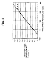
- a development potential is a difference between a development bias VB and the surface potential VL of a photoconductive element. Therefore, if the surface potential VL is constant, then the amount of toner deposition M/A is proportional to the development bias VB.
- the surface potential VL is a potential after exposure that is generally between 50 V and 100 V, and rises by about 50 V with the elapse of time.
- the surface potential VL drops in a low temperature, low humidity (LL) environment (usually 10°C and 15 %) or rises in a high temperature, high humidity (HH) environment (usually 27°C and 80 %).
- LL low temperature, low humidity
- HH high temperature, high humidity
- the surface potential VL is considered to vary little and be constant. It follows that the surface potential VL has little influence on the slope of the characteristic curve shown in FIG. 5. Particularly, in the case of toner as distinguished from a toner and carrier mixture, the slope of FIG. 5 is more stable because no consideration should be given to the "toner content of a developer".
- bias proportional coefficient amount of toner
- the deviation ⁇ VB of the bias for implementing the target amount of deposition from the bias used to form the test patch is produced by:
- the proportional coefficient k included in the Eq. (3) and corresponding to the slope of FIG. 6 is 133. Therefore, to achieve the target amount of toner deposition, it is necessary to determine the deviation VB of the bias for development. This is done in a step S35 by using the Eq. (3).
- the target amount of deposition is assumed to be the value VsA based on the sensor output, as stated above.
- the CPU 202 substitutes the value VB1 produced by the Eq. (4) for the value currently set in the development bias control unit 207.
- the CPU 202 writes the new value VB1 in the NVRAM 209 (step S37) and then ends the procedure.
- an image forming apparatus of the present invention is capable of accurately controlling the amount of toner deposition with a single patch and therefore in a short period of time with a minimum amount of toner deposition. Further, the apparatus minimizes the variation of a set value and thereby stably controls toner deposition to an optimal amount. This successfully obviates the fall of image quality and defective images and insures stable deposition conditions without regard to the elapse of time. Moreover, the apparatus brings the actual value to a target value and thereby enhances the above advantages. In addition, the apparatus accurately, simply corrects sensing means.
- the adjustment means preferably adjusts the set value by calculating an adjustment value based on which the set value is adjusted.
- the adjusting means adjusts the set value based on a predefined relationship between the amount of toner deposition and the sensor outputs.
- Said predefined relationship is in particular a linear relationship which may be described for instance by means of a proportional coefficient.
- different relationships between the sensor output and the amount of toner deposition are assumed in dependence on the colour of the toner (e.g. cyan magenta, yellow and black). In particular, in case of non-black (e.g.
- the sensitivity of the sensor means in particular with respect to non-black colours is adjusted before sensing the non-black colours.
- This adjustment of the sensitivity is preferably performed by changing the light intensity emitted by the light source of the sensing means and/or the response of the light detector of the light sensing means with respect to the reflected light.
- this adjustment of the sensitivity of the sensor means is performed by measuring reflectance of the black toner.
- the adjustment of the set value is based on a sensor output in case of sensing black toner and based on the sensor output in case of sensing non-black toner.
- the assumed and predefined relationships are preferably stored, e.g.
- the adjustment means performs first an adjustment of the sensitivity of the sensing means and then an adjustment of the set value based on the output of the adjusted sensing means, the sensitivity of which has been adjusted before.
- the sensitivity of the sensor means is in particular adjusted based on the sensor output, preferably, based on the difference between at least two sensor outputs obtained in case of sensing at least two different toner sensities.
- a high toner density which results in a saturated sensor signal and no toner density is used for obtaining the two output signals.
- black toner is sensed for adjusting the sensitivity of the sensor means.
- the present invention is also directed to a method for performing the adjustment of the set value as mentioned above and as described in an example in figure 3.
- the invention is further directed to a program which performs the method when it runs on a computer and to a computer medium which stores this program.
- the invention is directed to an image forming apparatus which comprises a controller which performs the afore-mentioned method.
Landscapes
- Engineering & Computer Science (AREA)
- Microelectronics & Electronic Packaging (AREA)
- Physics & Mathematics (AREA)
- General Physics & Mathematics (AREA)
- Control Or Security For Electrophotography (AREA)
- Dry Development In Electrophotography (AREA)
- Color Electrophotography (AREA)
Abstract
Description

Claims (5)
- An image forming apparatus comprising:wherein said sensing means uses a diffuse reflection system and has a correcting function; andan image carrier on which a developer is to be deposited by an electrophotographic system;control means for controlling an amount of the developer to deposit on said image carrier by varying a development potential;reflection type sensing means made up of a light source and a light-sensitive device for sensing the amount of the developer deposited on said image carrier; andadjusting means for adjusting a set value set in said control means for controlling the amount of the developer to a target value;
said adjusting means causes said sensing means to sense the amount of the developer deposited on a test patch, which is formed on the basis of a preselected set value, and calculates an adjustment value of the set value on the basis of said amount sensed by said sensing means and the target value and/or adjusts the set value based on the output of the sensing means and based on the target value and/or adjusts the sensitivity of the sensor means based on the sensor output. - The apparatus as claimed in claim 1, wherein said adjusting means causes the test patch to be formed on the basis of a current set value.
- The apparatus as claimed in claim 1 or 2, wherein said adjusting means calculates the adjustment value as a value proportional to a difference between the amount sensed by said sensing means and the target value.
- The apparatus as claimed in claim 1 or 2 or 3, wherein the correcting function of said sensing means performs correction on the basis of a value sensed when the developer is not deposited and a saturation value sensed when said developer is deposited.
- The apparatus as claimed in one of claims 1 to 4, further comprising developing means using a single-ingredient type developer.
Applications Claiming Priority (4)
| Application Number | Priority Date | Filing Date | Title |
|---|---|---|---|
| JP2001121455 | 2001-04-19 | ||
| JP2001121455 | 2001-04-19 | ||
| JP2002098232 | 2002-04-01 | ||
| JP2002098232A JP4107638B2 (en) | 2001-04-19 | 2002-04-01 | Image forming apparatus |
Publications (3)
| Publication Number | Publication Date |
|---|---|
| EP1251410A2 true EP1251410A2 (en) | 2002-10-23 |
| EP1251410A3 EP1251410A3 (en) | 2003-09-17 |
| EP1251410B1 EP1251410B1 (en) | 2009-11-18 |
Family
ID=26613861
Family Applications (1)
| Application Number | Title | Priority Date | Filing Date |
|---|---|---|---|
| EP02008270A Expired - Lifetime EP1251410B1 (en) | 2001-04-19 | 2002-04-19 | Image forming apparatus and control means for the amount of developer on the image carrier |
Country Status (4)
| Country | Link |
|---|---|
| US (1) | US6850718B2 (en) |
| EP (1) | EP1251410B1 (en) |
| JP (1) | JP4107638B2 (en) |
| DE (1) | DE60234404D1 (en) |
Cited By (1)
| Publication number | Priority date | Publication date | Assignee | Title |
|---|---|---|---|---|
| EP1804129A1 (en) * | 2005-12-28 | 2007-07-04 | Ricoh Company, Ltd. | Control of image quality adjustment at warm-up after energy-saving modus in an image froming apparatus |
Families Citing this family (11)
| Publication number | Priority date | Publication date | Assignee | Title |
|---|---|---|---|---|
| US7103166B2 (en) * | 2003-03-31 | 2006-09-05 | Sbc Properties, L.P. | Call transfer service using service control point and service node |
| CN100496640C (en) * | 2003-06-20 | 2009-06-10 | 学校法人庆应义塾 | Photodynamic therapy device, control method for photodynamic therapy device, and photodynamic therapy method |
| US20050134679A1 (en) * | 2003-12-04 | 2005-06-23 | Paterson Robert L. | Margin registration of a scan line in an electrophotographic printer |
| JP4631325B2 (en) * | 2004-06-28 | 2011-02-16 | 富士ゼロックス株式会社 | Image density adjusting apparatus and image forming apparatus using the same |
| JP2006133545A (en) * | 2004-11-08 | 2006-05-25 | Ricoh Co Ltd | Image forming apparatus |
| JP4782405B2 (en) * | 2004-11-15 | 2011-09-28 | 株式会社リコー | Image forming apparatus |
| JP4721401B2 (en) * | 2004-11-17 | 2011-07-13 | キヤノン株式会社 | Image forming apparatus and control method thereof |
| JP4695899B2 (en) * | 2005-03-14 | 2011-06-08 | キヤノン株式会社 | Image forming apparatus |
| JP2009025570A (en) * | 2007-07-19 | 2009-02-05 | Ricoh Co Ltd | Image forming apparatus, image carrier, and process cartridge |
| JP5262671B2 (en) * | 2008-12-16 | 2013-08-14 | 株式会社リコー | Image forming apparatus and image forming method |
| JP5929295B2 (en) * | 2012-02-21 | 2016-06-01 | セイコーエプソン株式会社 | Liquid ejector |
Family Cites Families (23)
| Publication number | Priority date | Publication date | Assignee | Title |
|---|---|---|---|---|
| JPS63148282A (en) * | 1986-12-12 | 1988-06-21 | Ricoh Co Ltd | Control method for image density |
| JPH02281269A (en) * | 1989-04-24 | 1990-11-16 | Ricoh Co Ltd | Image forming device |
| JP3172170B2 (en) * | 1990-08-20 | 2001-06-04 | 株式会社リコー | Image forming device |
| JP2584136B2 (en) | 1991-03-01 | 1997-02-19 | 松下電器産業株式会社 | Image forming device |
| JPH05302892A (en) | 1992-04-28 | 1993-11-16 | Fuji Xerox Co Ltd | Controlling system of density of image forming apparatus |
| JP2783940B2 (en) * | 1992-05-22 | 1998-08-06 | 三田工業株式会社 | Image forming device |
| US5605777A (en) | 1992-08-31 | 1997-02-25 | Ricoh Company, Ltd. | Method and apparatus for regenerating image holding member |
| JPH06148994A (en) | 1992-11-09 | 1994-05-27 | Ricoh Co Ltd | Image formation control device |
| JP2691512B2 (en) | 1993-09-22 | 1997-12-17 | 株式会社リコー | Method and apparatus for removing image forming substance from image carrier |
| JPH07140704A (en) | 1993-09-22 | 1995-06-02 | Ricoh Co Ltd | Repeated use of image carrier |
| JP3428091B2 (en) | 1993-10-03 | 2003-07-22 | 株式会社リコー | How to use the image carrier repeatedly |
| US5572293A (en) | 1993-10-14 | 1996-11-05 | Ricoh Company, Ltd. | Method of and system for cleaning a charge inducing member |
| JPH07114202A (en) | 1993-10-20 | 1995-05-02 | Ricoh Co Ltd | Image forming device |
| JPH07128956A (en) | 1993-11-05 | 1995-05-19 | Ricoh Co Ltd | Image forming device |
| EP0652492B1 (en) | 1993-11-09 | 1998-01-28 | Ricoh Company, Ltd | Image forming apparatus with a contact member contacting an image carrier |
| JP3337840B2 (en) * | 1994-04-26 | 2002-10-28 | キヤノン株式会社 | Concentration control method and apparatus |
| US5574538A (en) | 1994-09-26 | 1996-11-12 | Ricoh Company, Ltd. | Method and apparatus for removing image forming substance from image holding member forming processing situation mark |
| JP3761948B2 (en) | 1995-12-18 | 2006-03-29 | キヤノン株式会社 | Image processing apparatus and method |
| US5873011A (en) | 1996-03-13 | 1999-02-16 | Minolta Co., Ltd. | Image forming apparatus |
| JPH09319180A (en) | 1996-05-28 | 1997-12-12 | Ricoh Co Ltd | Toner supply control method in image forming apparatus |
| JP3991420B2 (en) * | 1997-03-27 | 2007-10-17 | 富士ゼロックス株式会社 | Image forming apparatus and control method thereof |
| JPH11258873A (en) | 1998-03-13 | 1999-09-24 | Toshiba Corp | Image forming apparatus and image forming method |
| JP3855524B2 (en) * | 1999-03-10 | 2006-12-13 | 富士ゼロックス株式会社 | Image forming apparatus |
-
2002
- 2002-04-01 JP JP2002098232A patent/JP4107638B2/en not_active Expired - Fee Related
- 2002-04-18 US US10/124,461 patent/US6850718B2/en not_active Expired - Fee Related
- 2002-04-19 EP EP02008270A patent/EP1251410B1/en not_active Expired - Lifetime
- 2002-04-19 DE DE60234404T patent/DE60234404D1/en not_active Expired - Lifetime
Cited By (2)
| Publication number | Priority date | Publication date | Assignee | Title |
|---|---|---|---|---|
| EP1804129A1 (en) * | 2005-12-28 | 2007-07-04 | Ricoh Company, Ltd. | Control of image quality adjustment at warm-up after energy-saving modus in an image froming apparatus |
| US7711275B2 (en) | 2005-12-28 | 2010-05-04 | Ricoh Company, Ltd. | Image forming apparatus having an imaging condition setting control |
Also Published As
| Publication number | Publication date |
|---|---|
| US20020172523A1 (en) | 2002-11-21 |
| JP4107638B2 (en) | 2008-06-25 |
| JP2003005465A (en) | 2003-01-08 |
| EP1251410B1 (en) | 2009-11-18 |
| US6850718B2 (en) | 2005-02-01 |
| EP1251410A3 (en) | 2003-09-17 |
| DE60234404D1 (en) | 2009-12-31 |
Similar Documents
| Publication | Publication Date | Title |
|---|---|---|
| US7684715B2 (en) | Image forming apparatus capable of stably maintaining an image density | |
| US5708917A (en) | Toner replenishment device for an image forming apparatus which employs pixel density and toner density information | |
| US6118557A (en) | Color image forming apparatus | |
| EP1049321B1 (en) | Image forming apparatus | |
| US5970276A (en) | Image forming apparatus and developer aging method | |
| US5424809A (en) | Image forming method and apparatus for the same | |
| US8229307B2 (en) | Image forming apparatus and image forming apparatus control method | |
| JPH0777866A (en) | Method for detection and correction with reference to low-development measure in every unit area | |
| US5237369A (en) | Color image forming equipment responsive to changes in ambient conditions | |
| US7539428B2 (en) | Image-forming device wherein the density of the images are corrected | |
| US20100067932A1 (en) | Image forming apparatus | |
| EP1251410B1 (en) | Image forming apparatus and control means for the amount of developer on the image carrier | |
| US5212560A (en) | Electrophotographic image forming apparatus comprising means for automatically adjusting image reproduction density | |
| US5873011A (en) | Image forming apparatus | |
| JPH06186816A (en) | Toner adhesion amount measuring method and image forming apparatus | |
| US5453773A (en) | Electrophotographic image forming apparatus comprising means for automatically adjusting image reproduction density | |
| US5499079A (en) | Image density control apparatus and method for controlling image density on a photoconductor surface | |
| US9684272B2 (en) | Image forming apparatus | |
| US5485191A (en) | Image forming apparatus having tone correcting function | |
| US7899348B2 (en) | Image forming apparatus with developing bias correcting portion that changes a developing density adjustment pattern | |
| JP2007286524A (en) | Image forming apparatus | |
| JP2021056421A (en) | Image forming apparatus | |
| JP4107550B2 (en) | Toner adhesion amount detection method, program, apparatus, and image forming apparatus | |
| JP4403726B2 (en) | Image forming apparatus and toner adhesion amount calculation method | |
| JP2002148887A (en) | Toner density measuring method and image forming device |
Legal Events
| Date | Code | Title | Description |
|---|---|---|---|
| PUAI | Public reference made under article 153(3) epc to a published international application that has entered the european phase |
Free format text: ORIGINAL CODE: 0009012 |
|
| 17P | Request for examination filed |
Effective date: 20020419 |
|
| AK | Designated contracting states |
Kind code of ref document: A2 Designated state(s): AT BE CH CY DE DK ES FI FR GB GR IE IT LI LU MC NL PT SE TR |
|
| AX | Request for extension of the european patent |
Free format text: AL;LT;LV;MK;RO;SI |
|
| PUAL | Search report despatched |
Free format text: ORIGINAL CODE: 0009013 |
|
| AK | Designated contracting states |
Kind code of ref document: A3 Designated state(s): AT BE CH CY DE DK ES FI FR GB GR IE IT LI LU MC NL PT SE TR |
|
| AX | Request for extension of the european patent |
Extension state: AL LT LV MK RO SI |
|
| RIC1 | Information provided on ipc code assigned before grant |
Ipc: 7G 03G 15/00 B Ipc: 7G 03G 15/08 A |
|
| AKX | Designation fees paid |
Designated state(s): DE FR GB |
|
| 17Q | First examination report despatched |
Effective date: 20060803 |
|
| RTI1 | Title (correction) |
Free format text: IMAGE FORMING APPARATUS AND CONTROL MEANS FOR THE AMOUNT OF DEVELOPER ON THE IMAGE CARRIER |
|
| GRAP | Despatch of communication of intention to grant a patent |
Free format text: ORIGINAL CODE: EPIDOSNIGR1 |
|
| GRAS | Grant fee paid |
Free format text: ORIGINAL CODE: EPIDOSNIGR3 |
|
| GRAA | (expected) grant |
Free format text: ORIGINAL CODE: 0009210 |
|
| AK | Designated contracting states |
Kind code of ref document: B1 Designated state(s): DE FR GB |
|
| REG | Reference to a national code |
Ref country code: GB Ref legal event code: FG4D |
|
| REF | Corresponds to: |
Ref document number: 60234404 Country of ref document: DE Date of ref document: 20091231 Kind code of ref document: P |
|
| PLBE | No opposition filed within time limit |
Free format text: ORIGINAL CODE: 0009261 |
|
| STAA | Information on the status of an ep patent application or granted ep patent |
Free format text: STATUS: NO OPPOSITION FILED WITHIN TIME LIMIT |
|
| 26N | No opposition filed |
Effective date: 20100819 |
|
| REG | Reference to a national code |
Ref country code: FR Ref legal event code: PLFP Year of fee payment: 14 |
|
| PGFP | Annual fee paid to national office [announced via postgrant information from national office to epo] |
Ref country code: GB Payment date: 20150420 Year of fee payment: 14 Ref country code: DE Payment date: 20150421 Year of fee payment: 14 |
|
| PGFP | Annual fee paid to national office [announced via postgrant information from national office to epo] |
Ref country code: FR Payment date: 20150421 Year of fee payment: 14 |
|
| REG | Reference to a national code |
Ref country code: DE Ref legal event code: R119 Ref document number: 60234404 Country of ref document: DE |
|
| GBPC | Gb: european patent ceased through non-payment of renewal fee |
Effective date: 20160419 |
|
| REG | Reference to a national code |
Ref country code: FR Ref legal event code: ST Effective date: 20161230 |
|
| PG25 | Lapsed in a contracting state [announced via postgrant information from national office to epo] |
Ref country code: FR Free format text: LAPSE BECAUSE OF NON-PAYMENT OF DUE FEES Effective date: 20160502 Ref country code: GB Free format text: LAPSE BECAUSE OF NON-PAYMENT OF DUE FEES Effective date: 20160419 Ref country code: DE Free format text: LAPSE BECAUSE OF NON-PAYMENT OF DUE FEES Effective date: 20161101 |