EP1249947A1 - Procédé et dispositif d'émission/réception à sauts de fréquence - Google Patents
Procédé et dispositif d'émission/réception à sauts de fréquence Download PDFInfo
- Publication number
- EP1249947A1 EP1249947A1 EP02290837A EP02290837A EP1249947A1 EP 1249947 A1 EP1249947 A1 EP 1249947A1 EP 02290837 A EP02290837 A EP 02290837A EP 02290837 A EP02290837 A EP 02290837A EP 1249947 A1 EP1249947 A1 EP 1249947A1
- Authority
- EP
- European Patent Office
- Prior art keywords
- data
- frequency
- block
- buffer
- carrier frequency
- Prior art date
- Legal status (The legal status is an assumption and is not a legal conclusion. Google has not performed a legal analysis and makes no representation as to the accuracy of the status listed.)
- Granted
Links
- 238000000034 method Methods 0.000 title claims abstract description 59
- 230000005540 biological transmission Effects 0.000 title claims abstract description 19
- 230000007704 transition Effects 0.000 claims abstract description 24
- 238000003780 insertion Methods 0.000 claims abstract description 3
- 230000037431 insertion Effects 0.000 claims abstract description 3
- 230000008569 process Effects 0.000 claims description 30
- 238000006243 chemical reaction Methods 0.000 claims description 25
- 230000008859 change Effects 0.000 claims description 11
- 230000006641 stabilisation Effects 0.000 abstract description 4
- 238000011105 stabilization Methods 0.000 abstract description 3
- 238000012360 testing method Methods 0.000 description 11
- 238000013519 translation Methods 0.000 description 4
- 241000135309 Processus Species 0.000 description 3
- 230000015572 biosynthetic process Effects 0.000 description 3
- 230000000903 blocking effect Effects 0.000 description 3
- 125000004122 cyclic group Chemical group 0.000 description 3
- 230000006870 function Effects 0.000 description 3
- 238000009877 rendering Methods 0.000 description 3
- 238000003786 synthesis reaction Methods 0.000 description 3
- 241001644893 Entandrophragma utile Species 0.000 description 2
- 238000012986 modification Methods 0.000 description 2
- 230000004048 modification Effects 0.000 description 2
- 238000012545 processing Methods 0.000 description 2
- 208000006379 syphilis Diseases 0.000 description 2
- 230000001131 transforming effect Effects 0.000 description 2
- 240000008042 Zea mays Species 0.000 description 1
- 238000012937 correction Methods 0.000 description 1
- 238000001514 detection method Methods 0.000 description 1
- 238000010586 diagram Methods 0.000 description 1
- 230000009977 dual effect Effects 0.000 description 1
- 229940082150 encore Drugs 0.000 description 1
- 239000003607 modifier Substances 0.000 description 1
- 238000011084 recovery Methods 0.000 description 1
- 238000000926 separation method Methods 0.000 description 1
- 230000009466 transformation Effects 0.000 description 1
Images




Classifications
-
- H—ELECTRICITY
- H04—ELECTRIC COMMUNICATION TECHNIQUE
- H04B—TRANSMISSION
- H04B1/00—Details of transmission systems, not covered by a single one of groups H04B3/00 - H04B13/00; Details of transmission systems not characterised by the medium used for transmission
- H04B1/69—Spread spectrum techniques
- H04B1/713—Spread spectrum techniques using frequency hopping
- H04B1/7156—Arrangements for sequence synchronisation
-
- H—ELECTRICITY
- H04—ELECTRIC COMMUNICATION TECHNIQUE
- H04B—TRANSMISSION
- H04B1/00—Details of transmission systems, not covered by a single one of groups H04B3/00 - H04B13/00; Details of transmission systems not characterised by the medium used for transmission
- H04B1/69—Spread spectrum techniques
- H04B1/713—Spread spectrum techniques using frequency hopping
- H04B1/7136—Arrangements for generation of hop frequencies, e.g. using a bank of frequency sources, using continuous tuning or using a transform
- H04B2001/71365—Arrangements for generation of hop frequencies, e.g. using a bank of frequency sources, using continuous tuning or using a transform using continuous tuning of a single frequency source
Definitions
- the present invention relates generally to a method and a device frequency hopping transmission and reception method and device correspondents.
- the present invention applies more particularly to frequency hopping telecommunications system transmitters / receivers.
- the Bluetooth telecommunications system is a universal radio interface low cost to replace wired or infrared links between different computer or electronic devices. This system operates in a band of frequency around 2.4 GHz and uses frequency hopping modulation. More specifically, during a connection between two Bluetooth entities, the data is transmitted in the form of blocks, the data of a block being transmitted at a radio frequency fixed for the entire duration of transmission of said block, radio frequencies succeeding each other according to a pseudo-random scheme.
- a platform universal and programmable radio (Software Defined Radio), capable of being configured on demand for a particular type of system.
- a platform consists of a microprocessor or a DSP processor, circuits Programmable FPGA (Field Programmable Gate Array), ASIC circuits with great configuration flexibility, as well as ADC converters and DAC. It is divided into a digital part and an analog part. The part digital is generally responsible, at transmission, for modulation and frequency translation of the baseband or the intermediate frequency to a radio frequency (RF) and reverse operation on reception.
- RF radio frequency
- the analog part is essentially responsible, on transmission, for digital-analog conversion and, conversely, on reception, of the analog-digital conversion.
- the realization of a frequency hopping system by means of a radio platform is delicate because the frequency synthesis circuit (DDS or Direct Digital Synthesizer), responsible for RF frequency generation, does not allow instantaneous switching from one RF frequency value to another. A certain stabilization time must indeed be respected.
- the presence of interpolator filters on transmission and reception decimators whose characteristics depend on the frequencies used, makes it difficult to program a frequency transition on a data well determined.
- the problem underlying the invention is to propose a radio platform for implementing a frequency hopping transmission / reception system universal, which does not have the aforementioned drawbacks.
- the problem is solved by the invention defined as a method of data transmission in the form of a series of blocks, each data block being subjected to frequency conversion to be transmitted to a carrier frequency, whereby when a first block of data intended to be transmitted at a first carrier frequency is followed by a second data block intended to be transmitted at a second carrier frequency, a sequence of stuffing data between the first block and the second block, the conversion of frequency passing from a conversion to the first carrier frequency to a conversion to the second carrier frequency when said frequency conversion operates on said padding data.
- the padding data are inserted under the form of a tamping block between said first and second blocks.
- the padding data are concatenated, as suffix, at the first padding block.
- the padding data are concatenated, as a prefix, to the second padding block.
- the method can include a first process of writing to a buffer of FIFO type and a second process to read this buffer, the first and the second process operating asynchronously.
- the first process writes a block of data when a flag indicates that the buffer is almost empty, then changes the flag value and start over.
- the second process meanwhile, reads data buffer, raise said flag if the buffer is almost empty, then start again.
- a blocking data block is written to the buffer if the next block must be transmitted at a carrier frequency different from the current carrier frequency.
- a padding suffix is concatenated with the block preceding the first block to be transmitted at a carrier frequency different from the current carrier frequency and the block thus concatenated is written to the buffer.
- a padding prefix is concatenated to a block of data if it is to be transmitted at a carrier frequency different from the current carrier frequency.
- the invention is also defined by an emission device adapted to transmit data in the form of a series of blocks and comprising means for implementing the method described above.
- the invention is further defined by a method for receiving transmitted data by a frequency hopping transmission device in the form of a series of blocks, each block having been transmitted at a carrier frequency being converted in baseband by means of frequency conversion, a first block of data, called useful, transmitted at a first carrier frequency, being separated from a second block of useful data, transmitted at a second carrier frequency, by a jam data sequence.
- a reception is detected on reception. transition between payload and stuffing data and that, if such a transition is detected, the frequency conversion changes from a conversion from the first carrier frequency to be converted from the second frequency carrier when said frequency conversion operates on said data of jam.
- the method comprises a first writing process in a FIFO type buffer and a second process for reading this buffer, the first and the second process operating asynchronously.
- the first process throws a flag when the buffer is almost full, then start again.
- the second process meanwhile, reads a data block when said flag indicates that the buffer is almost full, change the flag value, then start again.
- the second process determines the start of the second useful block after having detected a transition between payload and padding data and updates to each subsequent reading, the length of the current useful block remaining to be read.
- the invention finally relates to a reception device adapted to receive data transmitted by a frequency hopping transmission device and occurring in the form of useful data blocks, interspersed or not with sequences of padding data, said device comprising means for implementing the process as set out above.
- the device comprises a FIFO type buffer adapted to receive said data, a frequency converter operating at a frequency of work and suitable for converting the data read from said buffer into a band signal base, a frequency synthesizer providing said frequency converter with a signal at said working frequency, means adapted to detect a transition between useful data and stuffing data and a control device adapted to command said frequency synthesizer to change the working frequency when such a transition is detected.
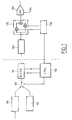
- Fig. 1 schematically illustrates the implementation of a frequency hopping transmitter, such as a Bluetooth transmitter, using a radio platform.
- This platform is divided into two independent modules working asynchronously, as indicated by the dashed line.
- the module on the left is entirely digital and is responsible for the transformation symbol bits.
- the module on the right called the rendering module, provides frequency translation at the carrier frequency.
- the digital module includes a modulator 130 transforming data coded NRZ to be transmitted in complex symbols (I, Q).
- the modulator 130 will be a GFSK (Gaussian Frequency Shift Keying) modulator in the case of a Bluetooth transmitter.
- the complex symbols provided by the modulator 130 will hereinafter be referred to as "useful data". These are stored as blocks of predetermined length in a buffer 110 using a Bi-FIFO memory.
- a Bi-FIFO memory is a memory of FIFO (First In First Out) type with dual read and write access ports. The buffer is filled by writing useful data from the digital module and is empty during reading by the rendering module.
- stuffing data 140 can be inserted between data blocks useful by means of the multiplexer 120. Useful data and padding data are then written in the Bi-FIFO buffer and read by the rendering module.
- a flag AEF (Almost Empty Flag) indicates the filling status of the buffer. More precisely, when the buffer is almost empty, i.e. when the size of the data stack stored is lower than a predetermined threshold value, the AEF flag (Almost Empty Flag) is raised.
- a control body 100 controls the entire digital module. In particular, the control body can read or change the value of the AEF flag, modify the state of the multiplexer 120, order the writing of useful or stuffing data in the buffer 110. In addition, the control unit 100 orders the restitution module the radio frequency jumps.
- the restitution module comprises an interpolator filter 160 in which the samples I and Q of the complex symbols are interpolated and a frequency converter 170 receiving two clocks in quadrature at the carrier frequency f 0 coming from a DDS generator (Direct Digital Synthetiser) 150
- the value of the carrier frequency f 0 is determined by the control unit 100.
- the frequency converter 170 translates the frequency of the signal represented by the baseband samples to the carrier frequency.
- the digital signal thus obtained is then converted into an analog signal by means of the digital / analog converter 180.
- the interpolator filter 160, the frequency synthesizer 150 and the frequency converter 170 are digital circuits.
- the interpolation, frequency synthesis and frequency conversion functions can be carried out by a processor of the digital module, the restitution module then being limited to digital / analog conversion.
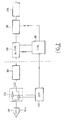
- the system illustrated in Fig. 2 schematically illustrates the implementation of a frequency hopping receiver, for example a Bluetooth receiver, using of a radio platform.
- This platform is divided into two modules freelancers, working asynchronously, as indicated by the line interrupted.
- the module on the left called the acquisition module, ensures the conversion analog / digital and frequency translation in baseband.
- the module right called digital module, is responsible for transforming symbols to bits, by example using a GFSK demodulator if a GFSK modulator was used transmission.
- the digital module can still provide other functions known per se, such as block synchronization, detection and correction errors, etc.
- the acquisition module comprises an analog / digital converter 280, a frequency converter 270 converting the radio-frequency signal from the converter 280 into a baseband signal.
- a frequency synthesizer 250 supplies the frequency converter 270 with two quadrature clocks at the carrier frequency (radio frequency) f 0 .
- the complex samples from the frequency converter 270 are decimated in the decimator 260 before being written to the Bi-FIFO buffer 210.
- the buffer is filled when writing data from the acquisition module and is emptied during their reading by the digital module.
- An AFF flag (Almost Full Flag) indicates the buffer filling status. More precisely, when the buffer is almost full, that is to say when the size of the stack of stored data is larger than a predetermined threshold value, the flag AFF is raised.
- a module 220 at the output of the buffer 210 is responsible for detecting the start of a block of useful data and for eliminating the padding data.
- the useful data is then converted into bits by the demodulator 230, for example a GFSK demodulator.
- a control unit 200 controls the entire digital module.
- the control unit can read or change the value of the AFF flag, order the reading of data in the buffer 210, order the module 220 to search for the start of a block of useful data.
- the controller 200 also determines the value of the carrier frequency generated by the synthesizer 250.
- the decimator filter 260, the frequency synthesizer 250 and the frequency converter 270 are digital circuits.
- the functions of frequency translation, frequency synthesis and decimation can be taken care of by a processor of the digital module, the acquisition module then being limited to analog / digital conversion.
- Fig. 3a illustrates a first alternative embodiment of the invention.
- the content of buffer 110 is schematically represented therein at successive instants.
- the instant (I) corresponds to the moment when the AEF flag has just passed 1.
- the end of a useful block D 0 is present in the buffer.
- the carrier frequency (radio frequency) chosen to transmit the data of block D 0 is f 0 .
- a first DD 0 stuffing block is first written to the buffer.
- the control unit 100 controls the multiplexer 120 so as to select a padding block from 140.
- the instant (II) corresponds to the moment when the first padding block has just been written in the buffer .
- the AEF flag is then set to 0 by the control body.
- the frequency cannot yet be modified because, given the delay through the interpolator filter 160, useful data of D 0 may still be present in the frequency converter 170.
- the buffer is again almost empty and the AEF flag is raised again.
- the control unit 100 then commands the writing of a second jamming block DD 1 , as can be seen in (IV), then orders the frequency synthesizer 150 to modify the carrier frequency to the value f 1 .
- the AEF flag is again set to 0.
- Fig. 3b illustrates a second variant of the invention.
- the instant (I) corresponds to the moment when the AEF flag has just passed 1.
- the end of a useful block D 0 is present in the buffer.
- the carrier frequency chosen to modulate the data of block D 0 is f 0 . If the transmitter has programmed a frequency change for the next useful block, a stuffing block DD 0 is then first written (II) in the buffer.
- the AEF flag is set to 0.
- the almost empty buffer trigger threshold must be taken sufficiently high and the size of the padding block chosen sufficiently large so that, on the one hand, when the buffer becomes almost again empty (III) of the jamming data is already in the frequency converter 170 and that, on the other hand, the frequency synthesizer has had time to stabilize while the jamming data is still in the frequency converter .
- the frequency of the synthesizer is modified to the value f 1 and the useful block to be transmitted at this new frequency is written in the buffer (IV).
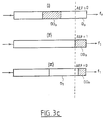
- Fig. 3c illustrates a third alternative embodiment of the invention.
- This variant differs from the previous one in that the variable length data block is authorized: the stuffing block is then concatenated as a suffix to the last block to be transmitted at the frequency f 0 .
- the suffix length and the almost empty buffer triggering threshold must be taken sufficiently high so that stuffing data is found in the frequency converter during the transition from f 0 to f 1 .
- the instant (I) shows the reading of the last useful block at the frequency f 0 .
- the buffer is almost empty and the stuffing data has already reached the frequency converter: the frequency is then modified to the value f 1 .
- the new useful block to be transmitted at this frequency is written (III) in the buffer.
- the concatenation of the suffix is controlled by the control member 100, by actuating the multiplexer 120, so as to allow the writing of a stuffing suffix following the useful data.
- Fig. 3d shows a fourth variant embodiment of the invention.
- This variant also assumes that the system authorizes the processing of blocks of variable length. It nevertheless differs from the previous one in that the stuffing data is no longer concatenated as a suffix to the last block to be transmitted at the frequency f 0 , but as a prefix to the first block to be transmitted at the new frequency f 1 .
- the instant (I) corresponds to the moment when the AEF flag has just passed 1.
- the end of a useful block D 0 to be modulated at the frequency f 0 is present in the buffer.
- the control unit 100 commands by the multiplexer 120 the writing of a prefix consisting of padding data, followed by the data of this useful block, then increases the almost empty buffer trigger threshold of a value + ⁇ and sets AEF to 0.
- the control unit 100 modifies the frequency to the value f 1 then restores the threshold triggering buffer almost empty at its initial value.
- the control unit orders the writing of a new useful block in the buffer.
- the value ⁇ and the size of the prefix must be chosen sufficiently large so that, on the one hand, when the buffer becomes almost empty with regard to an increased threshold value, the stuffing data has already reached the frequency converter and, on the other hand, when the buffer becomes almost empty again compared to the initial threshold value, stuffing data is still in the frequency converter.
- Fig. 4 shows possible contents of the buffer when AFF has just passed to 1.
- the limit corresponding to the buffer threshold has been shown in broken lines almost full.
- the dotted lines inside the buffer symbolize the separations between blocks or between a block and a prefix / suffix, as they are present at the show.
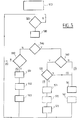
- Fig. 5 shows the flow diagram of the process for emptying the buffer 210 and recovery of useful data.
- each useful block begins with a particular sequence easily detectable (for example, by correlation) to differentiate it from a stuffing block.
- Step 510 symbolizes the initialization of the process: the remaining block length useful, r, is initialized to L, useful block length.
- We test in 540 if a useful block was being received: to do this, we compare the remaining useful block length, r, to the useful block length L. If r ⁇ L, this means that the rest of a useful block is expected, otherwise (r L), we wait for a new useful block.
- this method does not require a useful start of block search only after a frequency change because the system constantly monitors the value of remaining useful block length, r. If no useful block transition is detected while r is less than the width R of the reading window, a frequency jump must be done.
Landscapes
- Engineering & Computer Science (AREA)
- Computer Networks & Wireless Communication (AREA)
- Signal Processing (AREA)
- Mobile Radio Communication Systems (AREA)
- Radar Systems Or Details Thereof (AREA)
- Time-Division Multiplex Systems (AREA)
- Digital Transmission Methods That Use Modulated Carrier Waves (AREA)
- Medicines Containing Plant Substances (AREA)
- Developing Agents For Electrophotography (AREA)
Abstract
Description
- une donnée est lue du buffer 110 et fournie au filtre interpolateur 160 ;
- si le buffer est presque vide, le drapeau AEF est mis à 1 ;
- on retourne à la première étape .
- un bloc de données utiles est généré par modulateur 130 ;
- l'organe de contrôle 100 attend que le drapeau AEF soit à 1 ;
- lorsque le drapeau AEF est à 1, l'organe de contrôle 100 autorise l'écriture du bloc de données utiles dans le buffer 110 ;
- le drapeau AEF est mis à 0 et l'on retourne à la première étape.
L'idée générale à la base de l'invention est d'insérer un bloc de données de bourrage lorsqu'un saut de fréquence doit intervenir, de manière à ce que ces données de bourrage soient présentes dans le convertisseur de fréquence 170 lors du passage et la stabilisation à la nouvelle fréquence. Le processus de vidage du buffer reste inchangé, mais celui de remplissage doit être modifié, comme nous allons le voir, pour insérer les données de bourrage.
- les valeurs I et Q d'un échantillon complexe issu du décimateur sont écrites dans le buffer ;
- si le buffer est presque plein AFF est mis à 1 ;
- on retourne à la première étape.
- une transition entre blocs utiles ;
- aucune transition n'est observée, toutes les données de la fenêtre sont utiles ;
- une transition entre données utiles et données de bourrage, par exemple entre bloc utile et bloc de bourrage ou entre données utiles et suffixe de bourrage ;
- données de bourrage seules (bloc ou suffixe/préfixe de bourrage) ;
- une transition entre données de bourrage et données utiles, par exemple entre bloc de bourrage et bloc utile ou préfixe de bourrage et données utiles.
- dans l'affirmative, on se trouve dans la situation (1) de la Fig. 4. Toutes les données lues sont utiles et l'on passe à l'étape 561 de traitement des données lues puis à la mise à jour de r en 562. Enfin, on retourne à la boucle de test de AFF.
- dans la négative, on se trouve dans la situation (3) de la Fig. 4. L'organe de contrôle 200 ordonne, en 571, au synthétiseur 250 de modifier sa fréquence. La modification de fréquence intervient alors que des données de bourrage sont encore présentes dans le convertisseur de fréquence 270. Les r données utiles restantes sont traitées en 572 et la valeur r est réinitialisée à L en 573. En dernier lieu, on retourne à la boucle de test de AFF.
Claims (19)
- Procédé de transmission de données se présentant sous la forme d'une suite de blocs, chaque bloc de données étant soumis à une conversion de fréquence pour être transmis à une fréquence porteuse, caractérisé en ce lorsqu'un premier bloc de données destiné à être transmis à une première fréquence porteuse est suivi d'un second bloc de données destiné à être transmis à une seconde fréquence porteuse, l'on insère une séquence de données de bourrage entre le premier bloc et le second bloc et que la conversion de fréquence passe d'une conversion à la première fréquence porteuse à une conversion à la seconde fréquence porteuse lorsque ladite conversion de fréquence opère sur lesdites données de bourrage.
- Procédé selon la revendication 1, caractérisé en ce que les données de bourrage sont insérées sous la forme d'un bloc de bourrage entre lesdits premier et second blocs.
- Procédé selon la revendication 1, caractérisé en ce que les données de bourrage sont concaténées, comme suffixe, au premier bloc de bourrage.
- Procédé selon la revendication 1, caractérisé en ce que les données de bourrage sont concaténées, comme préfixe, au second bloc de bourrage.
- Procédé selon l'une des revendications précédentes, caractérisé en ce qu'il comprend un premier processus d'écriture dans un buffer (110) de type FIFO et un second processus de lecture de ce buffer, le premier et le second processus opérant de manière asynchrone.
- Procédé selon la revendication 5, caractérisé en ce que le premier processus écrit un bloc de données lorsqu'un drapeau (AEF) indique que le buffer est presque vide, puis change la valeur du drapeau et recommence.
- Procédé selon la revendication 6, caractérisé en ce que le second processus lit une donnée du buffer, lève ledit drapeau si le buffer est presque vide, puis recommence.
- Procédé selon les revendications 2 et 6, caractérisé en ce qu'un bloc de données de bourrage est écrit dans le buffer si le bloc suivant doit être transmis à une fréquence porteuse différente de la fréquence porteuse courante.
- Procédé selon les revendications 3 et 6, caractérisé en ce qu'un suffixe de bourrage est concaténé au bloc précédant le premier bloc devant être transmis à une fréquence porteuse différente de la fréquence porteuse courante et que le bloc ainsi concaténé est écrit dans le buffer.
- Procédé selon les revendications 4 et 6, caractérisé en ce qu'un préfixe de bourrage est concaténé à un bloc de données si celui-ci doit être transmis à une fréquence porteuse différente de la fréquence porteuse courante .
- Dispositif d'émission adapté à transmettre des données se présentant sous la forme d'une suite de blocs, caractérisé en ce qu'il comprend des moyens pour mettre en oeuvre le procédé selon l'une des revendications précédentes.
- Dispositif d'émission selon la revendication 11, caractérisé en ce qu'il comprend un buffer de type FIFO (110) adapté à recevoir des blocs de données à transmettre, un convertisseur de fréquence (170) adapté à transposer les données lues dudit buffer à une fréquence porteuse, un synthétiseur de fréquence (150) fournissant une horloge à la fréquence porteuse audit convertisseur (170), des moyens (120) d'insertion de données de bourrage, un organe de contrôle (100) adapté à commander aux dits moyens d'insertion d'insérer des données de bourrage entre deux blocs de données à transmettre et à commander au synthétiseur de fréquence un changement de fréquence porteuse.
- Procédé de réception de données émises par un dispositif d'émission à sauts de fréquence et se présentant sous la forme d'une suite de blocs, chaque bloc ayant été transmis à une fréquence porteuse étant converti en bande de base au moyen d'une conversion de fréquence, un premier bloc de données, dites utiles, transmis à une première fréquence porteuse, étant séparé d'un second bloc de données utiles, transmis à une seconde fréquence porteuse, par une séquence de données de bourrage, caractérisé en ce que l'on détecte à la réception une transition entre données utiles et données de bourrage et que, si une telle transition est détectée, la conversion de fréquence passe d'une conversion à partir de la première fréquence porteuse à une conversion à partir de la seconde fréquence porteuse lorsque ladite conversion de fréquence opère sur lesdites données de bourrage.
- Procédé selon la revendication 13, caractérisé en ce qu'il comprend un premier processus d'écriture dans un buffer de type FIFO et un second processus de lecture de ce buffer, le premier et le second processus opérant de manière asynchrone.
- Procédé selon la revendication 14, caractérisé en ce que le premier processus lève un drapeau (AFF) lorsque le buffer est presque plein, puis recommence.
- Procédé selon la revendication 15, caractérisé en ce que le second processus lit un bloc de données lorsque ledit drapeau indique que le buffer est presque plein, change la valeur du drapeau, puis recommence.
- Procédé selon l'une des revendications 13 à 16, caractérisé en ce que le second processus détermine le début du second bloc utile après avoir détecté une transition entre données utiles et données de bourrage et met à jour à chaque lecture suivante, la longueur du bloc utile courant restant à lire.
- Dispositif de réception adapté à recevoir des données émises par un dispositif d'émission à sauts de fréquence et se présentant sous la forme de blocs de données utiles, entrecoupés ou non par des séquences de données de bourrage, caractérisé en ce qu'il comprend des moyens pour mettre en oeuvre le procédé selon l'une des revendications 13 à 17.
- Dispositif de réception selon la revendication 18, caractérisé en ce qu'il comprend un buffer de type FIFO (210) adapté à recevoir lesdites données, un convertisseur de fréquence (270) opérant à une fréquence de travail et adapté à convertir les données lues dudit buffer en un signal en bande de base, un synthétiseur de fréquence (250) fournissant audit convertisseur de fréquence un signal à ladite fréquence de travail, des moyens (220) adaptés à détecter une transition entre données utiles et données de bourrage et un organe de contrôle (200) adapté à commander audit synthétiseur de fréquence un changement de la fréquence de travail lorsqu'une telle transition est détectée.
Applications Claiming Priority (2)
| Application Number | Priority Date | Filing Date | Title |
|---|---|---|---|
| FR0105153 | 2001-04-10 | ||
| FR0105153A FR2823403B1 (fr) | 2001-04-10 | 2001-04-10 | Procede et dispositif d'emission/reception a sauts de frequence |
Publications (2)
| Publication Number | Publication Date |
|---|---|
| EP1249947A1 true EP1249947A1 (fr) | 2002-10-16 |
| EP1249947B1 EP1249947B1 (fr) | 2006-11-15 |
Family
ID=8862368
Family Applications (1)
| Application Number | Title | Priority Date | Filing Date |
|---|---|---|---|
| EP02290837A Expired - Lifetime EP1249947B1 (fr) | 2001-04-10 | 2002-04-04 | Procédé et dispositif d'émission/réception à sauts de fréquence |
Country Status (7)
| Country | Link |
|---|---|
| US (1) | US7519100B2 (fr) |
| EP (1) | EP1249947B1 (fr) |
| JP (1) | JP4140689B2 (fr) |
| CN (1) | CN1166075C (fr) |
| AT (1) | ATE345602T1 (fr) |
| DE (1) | DE60215996T2 (fr) |
| FR (1) | FR2823403B1 (fr) |
Families Citing this family (1)
| Publication number | Priority date | Publication date | Assignee | Title |
|---|---|---|---|---|
| US7007114B1 (en) | 2003-01-31 | 2006-02-28 | Qlogic Corporation | System and method for padding data blocks and/or removing padding from data blocks in storage controllers |
Citations (3)
| Publication number | Priority date | Publication date | Assignee | Title |
|---|---|---|---|---|
| US5528623A (en) * | 1994-10-26 | 1996-06-18 | American Wireless Corporation | Cordless telephone system having automatic control of transmitter power and frequency in response to changing conditions |
| WO1996035265A1 (fr) * | 1995-05-04 | 1996-11-07 | Interwave Communications | Reseau de communication par etalement du spectre a souplesse d'adaptation en frequence |
| EP0785637A2 (fr) * | 1996-01-16 | 1997-07-23 | Canon Kabushiki Kaisha | Appareil et méthode de communication sans fils |
Family Cites Families (3)
| Publication number | Priority date | Publication date | Assignee | Title |
|---|---|---|---|---|
| US6130905A (en) * | 1996-07-03 | 2000-10-10 | Brother Kogyo Kabushiki Kaisha | Wireless communication system |
| US6172927B1 (en) * | 1997-04-01 | 2001-01-09 | Ramtron International Corporation | First-in, first-out integrated circuit memory device incorporating a retransmit function |
| DE19716011A1 (de) * | 1997-04-17 | 1998-10-22 | Abb Research Ltd | Verfahren und Vorrichtung zur Informationsübertragung über Stromversorgungsleitungen |
-
2001
- 2001-04-10 FR FR0105153A patent/FR2823403B1/fr not_active Expired - Lifetime
-
2002
- 2002-04-02 JP JP2002100022A patent/JP4140689B2/ja not_active Expired - Fee Related
- 2002-04-04 DE DE60215996T patent/DE60215996T2/de not_active Expired - Fee Related
- 2002-04-04 EP EP02290837A patent/EP1249947B1/fr not_active Expired - Lifetime
- 2002-04-04 AT AT02290837T patent/ATE345602T1/de not_active IP Right Cessation
- 2002-04-05 US US10/116,100 patent/US7519100B2/en not_active Expired - Fee Related
- 2002-04-10 CN CNB021206368A patent/CN1166075C/zh not_active Expired - Fee Related
Patent Citations (3)
| Publication number | Priority date | Publication date | Assignee | Title |
|---|---|---|---|---|
| US5528623A (en) * | 1994-10-26 | 1996-06-18 | American Wireless Corporation | Cordless telephone system having automatic control of transmitter power and frequency in response to changing conditions |
| WO1996035265A1 (fr) * | 1995-05-04 | 1996-11-07 | Interwave Communications | Reseau de communication par etalement du spectre a souplesse d'adaptation en frequence |
| EP0785637A2 (fr) * | 1996-01-16 | 1997-07-23 | Canon Kabushiki Kaisha | Appareil et méthode de communication sans fils |
Also Published As
| Publication number | Publication date |
|---|---|
| CN1166075C (zh) | 2004-09-08 |
| JP4140689B2 (ja) | 2008-08-27 |
| JP2003008477A (ja) | 2003-01-10 |
| FR2823403A1 (fr) | 2002-10-11 |
| DE60215996D1 (de) | 2006-12-28 |
| DE60215996T2 (de) | 2007-07-05 |
| US7519100B2 (en) | 2009-04-14 |
| CN1380755A (zh) | 2002-11-20 |
| US20020146061A1 (en) | 2002-10-10 |
| EP1249947B1 (fr) | 2006-11-15 |
| FR2823403B1 (fr) | 2003-06-13 |
| ATE345602T1 (de) | 2006-12-15 |
Similar Documents
| Publication | Publication Date | Title |
|---|---|---|
| EP0387948B1 (fr) | Circuit de prédistorsion adaptative à mémoire | |
| EP0159924B1 (fr) | Démodulateur DIDON numérique | |
| EP0421532A1 (fr) | Dispositif de prédistorsion pour système de transmission numérique | |
| FR2824215A1 (fr) | Procede et dispositif de traitement d'un message dans un reseau de communication | |
| FR2590099A1 (fr) | Procede pour transmettre une image de haute definition par un canal de communication a bande etroite | |
| FR2875358A1 (fr) | Insertion d'un flux secondaire d'informations binaires dans un flux principal de symboles d'une modulation numerique | |
| EP2345161B1 (fr) | Dispositif de reconstitution de l'horloge d'un signal nrz, et systeme de transmission associe | |
| EP1168634A1 (fr) | Procédé de réduction de la consommation électrique d'un téléphone mobile cellulaire | |
| EP1249947B1 (fr) | Procédé et dispositif d'émission/réception à sauts de fréquence | |
| US20130010902A1 (en) | Radio receiver, radio communication system, radio communication method, and program | |
| EP0541406A1 (fr) | Procédé et dispositif pour la transmission de deux informations dans le cadre d'une liaison dite à étalement de spectre | |
| FR2995115A1 (fr) | Procedes d'emission et de reception de donnees dans un systeme de telecommunications numeriques | |
| CA2144670C (fr) | Dispositif numerique de recuperation large bande d'une porteuse | |
| FR2997808A1 (fr) | Methode et dispositif de modulation numerique a faible densite de transitions | |
| EP0094040A2 (fr) | Système de transmission synchrone de données à l'aide d'une porteuse modulée d'amplitude d'enveloppe constante | |
| CA2125444A1 (fr) | Systeme de transmission numerique a etalement de spectre obtenu par codage pseudo-aleatoire basse frequence de l'information utile et procede d'etalement et de compression de spectre utilise dans un tel systeme | |
| EP1009105A1 (fr) | Récepteur, système de télécommunications CDMA et procédé de synchronisation d'un récepteur avec une station d'émission d'un tel système | |
| FR2919133A1 (fr) | Procede de detection de limite de trame et systeme de multiplexage | |
| EP1536566B1 (fr) | Circuit électronique de décodage d'un signal de données asynchrone biphase et procédé de décodage correspondant, dispositif de controle d'un équipement | |
| FR2781945A1 (fr) | Procede de codage convolutif et de transmission par paquets d'un flux serie de donnees numeriques, procede et dispositif de decodage correspondants | |
| EP1213872A2 (fr) | Récupération d'un paquet dans un système de transmissions par paquets avec voie de retour | |
| EP2388932A1 (fr) | Démodulateur pour transmission haut débit et procédéde démodulation correspondant. | |
| JP2009010754A (ja) | 並列サンプリング装置、並列サンプリング方法、受信装置及び受信方法 | |
| FR2894100A1 (fr) | Dispositif de reception numerique pour signaux codes dsss | |
| FR3022712A1 (fr) | Procede de demodulation auto-adaptative de signaux quasi-orthogonaux, unite de demodulation et recepteur de signaux radio |
Legal Events
| Date | Code | Title | Description |
|---|---|---|---|
| PUAI | Public reference made under article 153(3) epc to a published international application that has entered the european phase |
Free format text: ORIGINAL CODE: 0009012 |
|
| AK | Designated contracting states |
Kind code of ref document: A1 Designated state(s): AT BE CH CY DE DK ES FI FR GB GR IE IT LI LU MC NL PT SE TR |
|
| AX | Request for extension of the european patent |
Free format text: AL;LT;LV;MK;RO;SI |
|
| 17P | Request for examination filed |
Effective date: 20021118 |
|
| RAP1 | Party data changed (applicant data changed or rights of an application transferred) |
Owner name: MITSUBISHI ELECTRIC INFORMATION TECHNOLOGY CENTRE |
|
| AKX | Designation fees paid |
Designated state(s): AT BE CH CY DE DK ES FI FR GB GR IE IT LI LU MC NL PT SE TR |
|
| GRAP | Despatch of communication of intention to grant a patent |
Free format text: ORIGINAL CODE: EPIDOSNIGR1 |
|
| GRAS | Grant fee paid |
Free format text: ORIGINAL CODE: EPIDOSNIGR3 |
|
| GRAA | (expected) grant |
Free format text: ORIGINAL CODE: 0009210 |
|
| AK | Designated contracting states |
Kind code of ref document: B1 Designated state(s): AT BE CH CY DE DK ES FI FR GB GR IE IT LI LU MC NL PT SE TR |
|
| PG25 | Lapsed in a contracting state [announced via postgrant information from national office to epo] |
Ref country code: IT Free format text: LAPSE BECAUSE OF FAILURE TO SUBMIT A TRANSLATION OF THE DESCRIPTION OR TO PAY THE FEE WITHIN THE PRESCRIBED TIME-LIMIT;WARNING: LAPSES OF ITALIAN PATENTS WITH EFFECTIVE DATE BEFORE 2007 MAY HAVE OCCURRED AT ANY TIME BEFORE 2007. THE CORRECT EFFECTIVE DATE MAY BE DIFFERENT FROM THE ONE RECORDED. Effective date: 20061115 Ref country code: AT Free format text: LAPSE BECAUSE OF FAILURE TO SUBMIT A TRANSLATION OF THE DESCRIPTION OR TO PAY THE FEE WITHIN THE PRESCRIBED TIME-LIMIT Effective date: 20061115 Ref country code: NL Free format text: LAPSE BECAUSE OF FAILURE TO SUBMIT A TRANSLATION OF THE DESCRIPTION OR TO PAY THE FEE WITHIN THE PRESCRIBED TIME-LIMIT Effective date: 20061115 Ref country code: FI Free format text: LAPSE BECAUSE OF FAILURE TO SUBMIT A TRANSLATION OF THE DESCRIPTION OR TO PAY THE FEE WITHIN THE PRESCRIBED TIME-LIMIT Effective date: 20061115 Ref country code: IE Free format text: LAPSE BECAUSE OF FAILURE TO SUBMIT A TRANSLATION OF THE DESCRIPTION OR TO PAY THE FEE WITHIN THE PRESCRIBED TIME-LIMIT Effective date: 20061115 |
|
| REG | Reference to a national code |
Ref country code: GB Ref legal event code: FG4D Free format text: NOT ENGLISH |
|
| REG | Reference to a national code |
Ref country code: CH Ref legal event code: EP |
|
| REF | Corresponds to: |
Ref document number: 60215996 Country of ref document: DE Date of ref document: 20061228 Kind code of ref document: P |
|
| REG | Reference to a national code |
Ref country code: IE Ref legal event code: FG4D Free format text: LANGUAGE OF EP DOCUMENT: FRENCH |
|
| PG25 | Lapsed in a contracting state [announced via postgrant information from national office to epo] |
Ref country code: DK Free format text: LAPSE BECAUSE OF FAILURE TO SUBMIT A TRANSLATION OF THE DESCRIPTION OR TO PAY THE FEE WITHIN THE PRESCRIBED TIME-LIMIT Effective date: 20070215 Ref country code: SE Free format text: LAPSE BECAUSE OF FAILURE TO SUBMIT A TRANSLATION OF THE DESCRIPTION OR TO PAY THE FEE WITHIN THE PRESCRIBED TIME-LIMIT Effective date: 20070215 |
|
| PG25 | Lapsed in a contracting state [announced via postgrant information from national office to epo] |
Ref country code: ES Free format text: LAPSE BECAUSE OF FAILURE TO SUBMIT A TRANSLATION OF THE DESCRIPTION OR TO PAY THE FEE WITHIN THE PRESCRIBED TIME-LIMIT Effective date: 20070226 |
|
| GBT | Gb: translation of ep patent filed (gb section 77(6)(a)/1977) |
Effective date: 20070205 |
|
| PG25 | Lapsed in a contracting state [announced via postgrant information from national office to epo] |
Ref country code: PT Free format text: LAPSE BECAUSE OF FAILURE TO SUBMIT A TRANSLATION OF THE DESCRIPTION OR TO PAY THE FEE WITHIN THE PRESCRIBED TIME-LIMIT Effective date: 20070416 |
|
| NLV1 | Nl: lapsed or annulled due to failure to fulfill the requirements of art. 29p and 29m of the patents act | ||
| REG | Reference to a national code |
Ref country code: IE Ref legal event code: FD4D |
|
| PLBE | No opposition filed within time limit |
Free format text: ORIGINAL CODE: 0009261 |
|
| STAA | Information on the status of an ep patent application or granted ep patent |
Free format text: STATUS: NO OPPOSITION FILED WITHIN TIME LIMIT |
|
| 26N | No opposition filed |
Effective date: 20070817 |
|
| REG | Reference to a national code |
Ref country code: CH Ref legal event code: PL |
|
| BERE | Be: lapsed |
Owner name: MITSUBISHI ELECTRIC INFORMATION TECHNOLOGY CENTRE Effective date: 20070430 |
|
| PG25 | Lapsed in a contracting state [announced via postgrant information from national office to epo] |
Ref country code: LI Free format text: LAPSE BECAUSE OF NON-PAYMENT OF DUE FEES Effective date: 20070430 Ref country code: CH Free format text: LAPSE BECAUSE OF NON-PAYMENT OF DUE FEES Effective date: 20070430 |
|
| PG25 | Lapsed in a contracting state [announced via postgrant information from national office to epo] |
Ref country code: BE Free format text: LAPSE BECAUSE OF NON-PAYMENT OF DUE FEES Effective date: 20070430 |
|
| PG25 | Lapsed in a contracting state [announced via postgrant information from national office to epo] |
Ref country code: GR Free format text: LAPSE BECAUSE OF FAILURE TO SUBMIT A TRANSLATION OF THE DESCRIPTION OR TO PAY THE FEE WITHIN THE PRESCRIBED TIME-LIMIT Effective date: 20070216 |
|
| PG25 | Lapsed in a contracting state [announced via postgrant information from national office to epo] |
Ref country code: MC Free format text: LAPSE BECAUSE OF NON-PAYMENT OF DUE FEES Effective date: 20070430 |
|
| PGFP | Annual fee paid to national office [announced via postgrant information from national office to epo] |
Ref country code: GB Payment date: 20090313 Year of fee payment: 8 |
|
| PG25 | Lapsed in a contracting state [announced via postgrant information from national office to epo] |
Ref country code: CY Free format text: LAPSE BECAUSE OF FAILURE TO SUBMIT A TRANSLATION OF THE DESCRIPTION OR TO PAY THE FEE WITHIN THE PRESCRIBED TIME-LIMIT Effective date: 20061115 Ref country code: LU Free format text: LAPSE BECAUSE OF NON-PAYMENT OF DUE FEES Effective date: 20070404 |
|
| PGFP | Annual fee paid to national office [announced via postgrant information from national office to epo] |
Ref country code: DE Payment date: 20090415 Year of fee payment: 8 |
|
| PG25 | Lapsed in a contracting state [announced via postgrant information from national office to epo] |
Ref country code: TR Free format text: LAPSE BECAUSE OF FAILURE TO SUBMIT A TRANSLATION OF THE DESCRIPTION OR TO PAY THE FEE WITHIN THE PRESCRIBED TIME-LIMIT Effective date: 20061115 |
|
| REG | Reference to a national code |
Ref country code: FR Ref legal event code: ST Effective date: 20091231 |
|
| PG25 | Lapsed in a contracting state [announced via postgrant information from national office to epo] |
Ref country code: FR Free format text: LAPSE BECAUSE OF NON-PAYMENT OF DUE FEES Effective date: 20091222 |
|
| PGFP | Annual fee paid to national office [announced via postgrant information from national office to epo] |
Ref country code: FR Payment date: 20080422 Year of fee payment: 7 |
|
| GBPC | Gb: european patent ceased through non-payment of renewal fee |
Effective date: 20100404 |
|
| PG25 | Lapsed in a contracting state [announced via postgrant information from national office to epo] |
Ref country code: DE Free format text: LAPSE BECAUSE OF NON-PAYMENT OF DUE FEES Effective date: 20101103 |
|
| PG25 | Lapsed in a contracting state [announced via postgrant information from national office to epo] |
Ref country code: GB Free format text: LAPSE BECAUSE OF NON-PAYMENT OF DUE FEES Effective date: 20100404 |