EP1249904A2 - Group III nitride compound semiconductor laser and manufacturing method thereof - Google Patents
Group III nitride compound semiconductor laser and manufacturing method thereof Download PDFInfo
- Publication number
- EP1249904A2 EP1249904A2 EP02008015A EP02008015A EP1249904A2 EP 1249904 A2 EP1249904 A2 EP 1249904A2 EP 02008015 A EP02008015 A EP 02008015A EP 02008015 A EP02008015 A EP 02008015A EP 1249904 A2 EP1249904 A2 EP 1249904A2
- Authority
- EP
- European Patent Office
- Prior art keywords
- layer
- compound semiconductor
- nitride compound
- semiconductor laser
- current constricting
- Prior art date
- Legal status (The legal status is an assumption and is not a legal conclusion. Google has not performed a legal analysis and makes no representation as to the accuracy of the status listed.)
- Granted
Links
Images


Classifications
-
- H—ELECTRICITY
- H01—ELECTRIC ELEMENTS
- H01S—DEVICES USING THE PROCESS OF LIGHT AMPLIFICATION BY STIMULATED EMISSION OF RADIATION [LASER] TO AMPLIFY OR GENERATE LIGHT; DEVICES USING STIMULATED EMISSION OF ELECTROMAGNETIC RADIATION IN WAVE RANGES OTHER THAN OPTICAL
- H01S5/00—Semiconductor lasers
- H01S5/30—Structure or shape of the active region; Materials used for the active region
- H01S5/32—Structure or shape of the active region; Materials used for the active region comprising PN junctions, e.g. hetero- or double- heterostructures
- H01S5/323—Structure or shape of the active region; Materials used for the active region comprising PN junctions, e.g. hetero- or double- heterostructures in AIIIBV compounds, e.g. AlGaAs-laser, InP-based laser
- H01S5/32308—Structure or shape of the active region; Materials used for the active region comprising PN junctions, e.g. hetero- or double- heterostructures in AIIIBV compounds, e.g. AlGaAs-laser, InP-based laser emitting light at a wavelength less than 900 nm
- H01S5/32341—Structure or shape of the active region; Materials used for the active region comprising PN junctions, e.g. hetero- or double- heterostructures in AIIIBV compounds, e.g. AlGaAs-laser, InP-based laser emitting light at a wavelength less than 900 nm blue laser based on GaN or GaP
-
- H—ELECTRICITY
- H01—ELECTRIC ELEMENTS
- H01S—DEVICES USING THE PROCESS OF LIGHT AMPLIFICATION BY STIMULATED EMISSION OF RADIATION [LASER] TO AMPLIFY OR GENERATE LIGHT; DEVICES USING STIMULATED EMISSION OF ELECTROMAGNETIC RADIATION IN WAVE RANGES OTHER THAN OPTICAL
- H01S2301/00—Functional characteristics
- H01S2301/18—Semiconductor lasers with special structural design for influencing the near- or far-field
-
- H—ELECTRICITY
- H01—ELECTRIC ELEMENTS
- H01S—DEVICES USING THE PROCESS OF LIGHT AMPLIFICATION BY STIMULATED EMISSION OF RADIATION [LASER] TO AMPLIFY OR GENERATE LIGHT; DEVICES USING STIMULATED EMISSION OF ELECTROMAGNETIC RADIATION IN WAVE RANGES OTHER THAN OPTICAL
- H01S2304/00—Special growth methods for semiconductor lasers
-
- H—ELECTRICITY
- H01—ELECTRIC ELEMENTS
- H01S—DEVICES USING THE PROCESS OF LIGHT AMPLIFICATION BY STIMULATED EMISSION OF RADIATION [LASER] TO AMPLIFY OR GENERATE LIGHT; DEVICES USING STIMULATED EMISSION OF ELECTROMAGNETIC RADIATION IN WAVE RANGES OTHER THAN OPTICAL
- H01S5/00—Semiconductor lasers
- H01S5/02—Structural details or components not essential to laser action
- H01S5/0206—Substrates, e.g. growth, shape, material, removal or bonding
- H01S5/0213—Sapphire, quartz or diamond based substrates
-
- H—ELECTRICITY
- H01—ELECTRIC ELEMENTS
- H01S—DEVICES USING THE PROCESS OF LIGHT AMPLIFICATION BY STIMULATED EMISSION OF RADIATION [LASER] TO AMPLIFY OR GENERATE LIGHT; DEVICES USING STIMULATED EMISSION OF ELECTROMAGNETIC RADIATION IN WAVE RANGES OTHER THAN OPTICAL
- H01S5/00—Semiconductor lasers
- H01S5/02—Structural details or components not essential to laser action
- H01S5/022—Mountings; Housings
- H01S5/0233—Mounting configuration of laser chips
- H01S5/0234—Up-side down mountings, e.g. Flip-chip, epi-side down mountings or junction down mountings
-
- H—ELECTRICITY
- H01—ELECTRIC ELEMENTS
- H01S—DEVICES USING THE PROCESS OF LIGHT AMPLIFICATION BY STIMULATED EMISSION OF RADIATION [LASER] TO AMPLIFY OR GENERATE LIGHT; DEVICES USING STIMULATED EMISSION OF ELECTROMAGNETIC RADIATION IN WAVE RANGES OTHER THAN OPTICAL
- H01S5/00—Semiconductor lasers
- H01S5/20—Structure or shape of the semiconductor body to guide the optical wave ; Confining structures perpendicular to the optical axis, e.g. index or gain guiding, stripe geometry, broad area lasers, gain tailoring, transverse or lateral reflectors, special cladding structures, MQW barrier reflection layers
- H01S5/22—Structure or shape of the semiconductor body to guide the optical wave ; Confining structures perpendicular to the optical axis, e.g. index or gain guiding, stripe geometry, broad area lasers, gain tailoring, transverse or lateral reflectors, special cladding structures, MQW barrier reflection layers having a ridge or stripe structure
- H01S5/2205—Structure or shape of the semiconductor body to guide the optical wave ; Confining structures perpendicular to the optical axis, e.g. index or gain guiding, stripe geometry, broad area lasers, gain tailoring, transverse or lateral reflectors, special cladding structures, MQW barrier reflection layers having a ridge or stripe structure comprising special burying or current confinement layers
- H01S5/2206—Structure or shape of the semiconductor body to guide the optical wave ; Confining structures perpendicular to the optical axis, e.g. index or gain guiding, stripe geometry, broad area lasers, gain tailoring, transverse or lateral reflectors, special cladding structures, MQW barrier reflection layers having a ridge or stripe structure comprising special burying or current confinement layers based on III-V materials
- H01S5/221—Structure or shape of the semiconductor body to guide the optical wave ; Confining structures perpendicular to the optical axis, e.g. index or gain guiding, stripe geometry, broad area lasers, gain tailoring, transverse or lateral reflectors, special cladding structures, MQW barrier reflection layers having a ridge or stripe structure comprising special burying or current confinement layers based on III-V materials containing aluminium
-
- H—ELECTRICITY
- H01—ELECTRIC ELEMENTS
- H01S—DEVICES USING THE PROCESS OF LIGHT AMPLIFICATION BY STIMULATED EMISSION OF RADIATION [LASER] TO AMPLIFY OR GENERATE LIGHT; DEVICES USING STIMULATED EMISSION OF ELECTROMAGNETIC RADIATION IN WAVE RANGES OTHER THAN OPTICAL
- H01S5/00—Semiconductor lasers
- H01S5/20—Structure or shape of the semiconductor body to guide the optical wave ; Confining structures perpendicular to the optical axis, e.g. index or gain guiding, stripe geometry, broad area lasers, gain tailoring, transverse or lateral reflectors, special cladding structures, MQW barrier reflection layers
- H01S5/22—Structure or shape of the semiconductor body to guide the optical wave ; Confining structures perpendicular to the optical axis, e.g. index or gain guiding, stripe geometry, broad area lasers, gain tailoring, transverse or lateral reflectors, special cladding structures, MQW barrier reflection layers having a ridge or stripe structure
- H01S5/2205—Structure or shape of the semiconductor body to guide the optical wave ; Confining structures perpendicular to the optical axis, e.g. index or gain guiding, stripe geometry, broad area lasers, gain tailoring, transverse or lateral reflectors, special cladding structures, MQW barrier reflection layers having a ridge or stripe structure comprising special burying or current confinement layers
- H01S5/2214—Structure or shape of the semiconductor body to guide the optical wave ; Confining structures perpendicular to the optical axis, e.g. index or gain guiding, stripe geometry, broad area lasers, gain tailoring, transverse or lateral reflectors, special cladding structures, MQW barrier reflection layers having a ridge or stripe structure comprising special burying or current confinement layers based on oxides or nitrides
- H01S5/2216—Structure or shape of the semiconductor body to guide the optical wave ; Confining structures perpendicular to the optical axis, e.g. index or gain guiding, stripe geometry, broad area lasers, gain tailoring, transverse or lateral reflectors, special cladding structures, MQW barrier reflection layers having a ridge or stripe structure comprising special burying or current confinement layers based on oxides or nitrides nitrides
-
- H—ELECTRICITY
- H01—ELECTRIC ELEMENTS
- H01S—DEVICES USING THE PROCESS OF LIGHT AMPLIFICATION BY STIMULATED EMISSION OF RADIATION [LASER] TO AMPLIFY OR GENERATE LIGHT; DEVICES USING STIMULATED EMISSION OF ELECTROMAGNETIC RADIATION IN WAVE RANGES OTHER THAN OPTICAL
- H01S5/00—Semiconductor lasers
- H01S5/20—Structure or shape of the semiconductor body to guide the optical wave ; Confining structures perpendicular to the optical axis, e.g. index or gain guiding, stripe geometry, broad area lasers, gain tailoring, transverse or lateral reflectors, special cladding structures, MQW barrier reflection layers
- H01S5/22—Structure or shape of the semiconductor body to guide the optical wave ; Confining structures perpendicular to the optical axis, e.g. index or gain guiding, stripe geometry, broad area lasers, gain tailoring, transverse or lateral reflectors, special cladding structures, MQW barrier reflection layers having a ridge or stripe structure
- H01S5/2205—Structure or shape of the semiconductor body to guide the optical wave ; Confining structures perpendicular to the optical axis, e.g. index or gain guiding, stripe geometry, broad area lasers, gain tailoring, transverse or lateral reflectors, special cladding structures, MQW barrier reflection layers having a ridge or stripe structure comprising special burying or current confinement layers
- H01S5/2218—Structure or shape of the semiconductor body to guide the optical wave ; Confining structures perpendicular to the optical axis, e.g. index or gain guiding, stripe geometry, broad area lasers, gain tailoring, transverse or lateral reflectors, special cladding structures, MQW barrier reflection layers having a ridge or stripe structure comprising special burying or current confinement layers having special optical properties
- H01S5/222—Structure or shape of the semiconductor body to guide the optical wave ; Confining structures perpendicular to the optical axis, e.g. index or gain guiding, stripe geometry, broad area lasers, gain tailoring, transverse or lateral reflectors, special cladding structures, MQW barrier reflection layers having a ridge or stripe structure comprising special burying or current confinement layers having special optical properties having a refractive index lower than that of the cladding layers or outer guiding layers
-
- H—ELECTRICITY
- H01—ELECTRIC ELEMENTS
- H01S—DEVICES USING THE PROCESS OF LIGHT AMPLIFICATION BY STIMULATED EMISSION OF RADIATION [LASER] TO AMPLIFY OR GENERATE LIGHT; DEVICES USING STIMULATED EMISSION OF ELECTROMAGNETIC RADIATION IN WAVE RANGES OTHER THAN OPTICAL
- H01S5/00—Semiconductor lasers
- H01S5/20—Structure or shape of the semiconductor body to guide the optical wave ; Confining structures perpendicular to the optical axis, e.g. index or gain guiding, stripe geometry, broad area lasers, gain tailoring, transverse or lateral reflectors, special cladding structures, MQW barrier reflection layers
- H01S5/22—Structure or shape of the semiconductor body to guide the optical wave ; Confining structures perpendicular to the optical axis, e.g. index or gain guiding, stripe geometry, broad area lasers, gain tailoring, transverse or lateral reflectors, special cladding structures, MQW barrier reflection layers having a ridge or stripe structure
- H01S5/2205—Structure or shape of the semiconductor body to guide the optical wave ; Confining structures perpendicular to the optical axis, e.g. index or gain guiding, stripe geometry, broad area lasers, gain tailoring, transverse or lateral reflectors, special cladding structures, MQW barrier reflection layers having a ridge or stripe structure comprising special burying or current confinement layers
- H01S5/2222—Structure or shape of the semiconductor body to guide the optical wave ; Confining structures perpendicular to the optical axis, e.g. index or gain guiding, stripe geometry, broad area lasers, gain tailoring, transverse or lateral reflectors, special cladding structures, MQW barrier reflection layers having a ridge or stripe structure comprising special burying or current confinement layers having special electric properties
Definitions
- This invention relates to a nitride compound semiconductor laser (hereafter, may be simply referred to device) having a plurality of crystal layers of group III nitride compound semiconductor expressed by the formula (Al x Ga 1-x ) 1-y In y N(0 ⁇ x ⁇ 1, 0 ⁇ y ⁇ 1), to which carriers are supplied from electrodes. More specifically, this invention relates to a group III nitride compound semiconductor laser that can emit laser light of wavelengths ranging from ultra-violet to blue and to a method for manufacturing the same.
- a number of possible structures for semiconductor laser have been proposed over the years. Many of them include structures for limiting the area for current injection in the direction parallel to the pn junction, namely transverse direction, and those for confining light generated in the active layer in the transverse direction. Those structures typically break down into two types: the ridge-type, namely mesa-stripe type; and the inner stripe type, namely the internal current flow restriction type.
- the ridge-type semiconductor laser has the so-called ridge-type structure in which a stripe-shape narrow bump is formed in a region above a p-type guide layer and a p-side electrode is formed on this bump.
- the device of this type needs a high-precision process of the ridge structure. This process consists of numerous steps and makes it difficult to improve the manufacturing yield of the device. This is because the dimensions of the ridge structure significantly influence the threshold current for oscillation and lightbeam quality.
- Japanese Patent Kokai No. Hei. 11-261160 discloses a group III nitride compound semiconductor laser of an inner stripe type that has a pair of clad layers, an active layer sandwiched between the clad layers and a current constricting layer having a stripe-shape aperture serving as the path for current over the active layer.
- This current constricting layer is a highly resistant layer that is fabricated by heating an amorphous or poly-crystalline nitride compound semiconductor layer and then crystallizing this layer.
- This current constricting layer is made of GaN containing impurities at least 1x10 20 cm -3 . The light is confined in the transverse direction by utilizing the light absorption effect relevant to the impurity energy states in this layer.
- the clad layer over the aperture of the current constricting layer is regrown on the uneven (bumpy) underlying layer.
- the distribution of Mg concentration is not uniform in the semiconductor layer of the aperture and then its electric performance deteriorates.
- the satisfactory p-type conduction is realized when the Mg concentration is within a very limited range. Thus if there are fluctuations in the distribution of Mg concentration, the p-type conduction properties deteriorate.
- An object of the present invention is, therefore, to provide an inner stripe type nitride compound semiconductor laser that can be driven at low current and voltage, easy to manufacture and stable during operation at the transverse mode of light.
- the present invention provides a group III nitride compound semiconductor laser that has a pair of opposing guide and clad layers sandwiching an active layer and a current constricting layer located intermediate in a p-type guide layer.
- the current constricting layer is made of AlN deposited at low temperatures between 400-600°C and has a stripe-shape aperture that restricts the area through which current is injected to the active layer.
- the nitride compound semiconductor laser according to the present invention is a nitride compound semiconductor laser having a plurality of crystal layers made of a group III nitride compound semiconductor expressed by the formula (Al x Ga 1-x ) 1-y In y N (where 0 ⁇ x ⁇ 1, 0 ⁇ y ⁇ 1), the plurality of crystal layers comprising an active layer-side guide layer which is adjacent to the active layer in the crystal layers of the group III nitride compound semiconductor and made of Al x ,Ga 1-x'-y' In y' N (where 0 ⁇ x' ⁇ 1, 0 ⁇ y' ⁇ 1), a current constricting AlN layer which is deposited on said guide layer and has a stripe-shape aperture, an electrode-side guide layer which is made of Al x'' Ga 1-x
- the band gaps of the active layer-side guide layer, the electrode-side guide layer and the clad layer are represented by Eg1, Eg2 and Eg3, respectively, their relations are Eg1 ⁇ Eg2 ⁇ Eg3.
- the guide layer on the active layer side and the guide layer on the electrode side may have the same composition, Al x Ga 1-x-y In y N (where 0 ⁇ x ⁇ 1, 0 ⁇ y ⁇ 1).
- a semiconductor layer of Al z Ga 1-z N (where 0.05 ⁇ z ⁇ 0.3) may be formed immediately above the active layer of the device in order to protect the active layer and prevent the overflow of electrons.
- the film thickness of the current constricting AlN layer is 100-800 ⁇ , preferably 200-600 ⁇ in the present invention. Since the refractive index of the AlN layer is approximately 2.15 and smaller than those of the other regions, an effective step of the refractive index is provided that can confine light in the horizontal direction (transverse direction) parallel to the pn junction in the vicinity of the aperture of the current constricting layer.
- the light confinement in the transverse direction is different from the conventional one utilizing the current constricting layer where impurities have been heavily doped to provide an appropriate absorption coefficient for the light emitted from the active layer.
- the present invention utilizes an effective step of the refractive index resulting from an appropriate low refractive index of AlN.
- the AlN film deposited at low temperatures is amorphous (non-crystal) and this layer is used as a buffer layer that relaxes mismatching in the lattice constant when growing GaN on the sapphire substrate. Therefore, it is easy to regrow GaN:Mg layer(p-type guide layer) on the low temperature deposited AlN layer. If the AlN film is thicker than the upper limit, 800 ⁇ , it becomes almost impossible to sufficiently flatten by the deposition of the electrode-side guide layer. Group II elements such as Mg are added to the guide layer, and the guide layer comes to show p-type conduction through annealing treatment.
- the current constricting layer made of AlN is located inside the p-type guide layer.
- this structure can avoid the conventional problem that the current-voltage properties deteriorate due to the increase of the electric resistance of the p-type crystal layer within the aperture of the current constricting layer.
- the Mg distribution in the p-type crystal layer within the aperture of the current constricting layer becomes inhomogeneous during the growth of the p-type guide layer as well.
- the resulting current-voltage properties of the device are good.
- the band gap of the guide layer is designed to be smaller than that of the clad layer and a large number of carriers (in this case, holes) can flow into the guide layer from the clad layer to provide a high conductivity for the guide layer when the device is forward-biased. Therefore, if the clad layer is a good p-type layer, a sufficient number of carriers are supplied from the clad layer. This explanation is consistent with the fact that laser oscillation is realized even if the guide layer is undoped.
- the semiconductor laser of the inner stripe type according to the present invention provides another merit that it is easy to attain a thermally preferable contact when mounting the device on a heat sink with its p-side down.
- AlN has a merit in terms of heat dissipation because it has a thermal conductivity of 285W/mK around at room temperature, which is more than twice the thermal conductivity of GaN, 130W/mK.
- This feature of AlN is a merit whether the device is mounted on the heat sink with the p-side up or p-side down, thus contributing to a longer life of use.
- the current constricting layer made of AlN can be etched by wet process and it is easy to form the aperture.
- the device manufacturing method disclosed in Japanese Patent Kokai No. Hei. 11-261160 describes that the etching becomes difficult to perform when forming a Ga x Al y In 1-x-y N(0 ⁇ x, y ⁇ 1) film if its Al content is high because of its higher etchingresistance.
- the wet etching of AlN formed on the p-type GaN provides a highly clean surface.
- the interface resulting from this film regrowth does not work as a barrier that contains too many impurities.
- the growth of these crystal layers is conducted by the metalorganic chemical vapor deposition method.
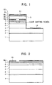
- Fig. 1 shows an example of semiconductor lasers using group III nitride compound semiconductor, which is an inner stripe type laser device of the separate confinement heterostructure (SCH).
- Denoted 1 is a single-crystal sapphire substrate, 2 a GaN (or AlN) buffer layer deposited at low temperatures, 3 an n-type GaN contact layer, 4 an n-type Al 0.08 Ga 0.92 N clad layer, 5 an n-type GaN guide layer, 6 an active layer of, for example, the multiple quantum well (MQW) structure having InGaN as the major constituting element, 7 a p-type Al 0.2 Ga 0.8 N electron barrier layer or cap layer, 8a a p-type GaN guide layer on the active layer side, 8c a current constricting AlN layer, 8b a p-type GaN guide layer on the electrode side, 9 a p-type Al 0.08 Ga 0.92 N clad layer, 10 a p-type GaN contact layer where group II impurities such
- the active layer 6 emits light when electrons and holes supplied from the electrodes recombine each other.
- the n-type and p-type GaN guide layers 5, 8a, 8b guide the light generated in the active layer 6.
- the electrons and holes are effectively confined in the active layer 6 by controlling the band gaps of the guide layers to be larger than that of the active layer 6.
- the p-type electron barrier layer or cap layer 7 is the barrier layer that strengthens the confinement of injected carriers (particularly, electrons) and may prevent the vaporization of the active layer when the active layer 6 grown at 700-800°C is heated up to 1000-1100°C.
- the n-type contact layer 3 is an underlying layer formed as the current path because the sapphire substrate is not electrically conductive at all.
- the buffer layer 2 grown at low temperatures is formed so as to deposit a flat film on the sapphire substrate that is a foreign material to GaN.
- the current-voltage characteristics of the device fabricated according to the present invention were measured.
- Fig. 5 shows the measurement results (solid line).
- measured were the current-voltage characteristics of a device that was fabricated in the same way as the above embodiment except that the electrode-side guide layer was not formed but only the clad layer made of Al 0.08 Ga 0.92 N;Mg was regrown (dotted line in Fig. 5). Comparing these characteristics, it is found that the turnon voltage is lower in the device fabricated according to the embodiment. Besides, the voltage in the device of the present invention is lower about 1.5-2.0 volts than that in the device of the comparative example in the device operating current range 40-120mA. Thus the device fabricated according to the present invention is advantageous in terms of operating voltage.
- the lasing threshold current was 46mA, voltage 5V and halfwidth 7 degrees for the transverse FFP.
- the operation of the invented device was stable even after a continuous operation of 100 hours or longer at a light output power of 30mW. This performance is high enough for practical use.
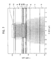
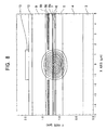
- FIG. 7 and Fig. 8 A simulation study was conducted to confirm the current flow constriction and light confinement effects in the device of the present invention.
- the device structure was assumed to be the same as that of the above embodiment except that the film thickness of the p-type electrode-side guide layer was 500 ⁇ .
- the composition of each layer was assumed to be the same as that of the embodiment.
- a simulation was conducted assuming that AlN had a refractive index of 2.15 and was a dielectric material.
- the simulation results are demonstrated in Fig. 7 and Fig. 8. Referring to Fig. 7 and Fig. 8, the horizontal axis (X-axis) represents the horizontal position in ⁇ m with reference to the center of the device, while the vertical axis (Y-axis) represents the relative position in ⁇ m in the direction the film layers are deposited.
- Fig. 7 is a diagram showing the distribution of current density in a cross-section of the device.
- the size of each triangle represents the magnitude of current density.
- the diagram indicates that the current spread in the transverse direction in the active layer is restricted to the same width as that of the aperture of the current constricting layer made of AlN.
- Fig. 8 is a diagram illustrating the strength distribution of electric field of light in the cross-section of the device with contour lines. If the strength of electric field of the most inward line is scaled 100, that of the most outward line is 10. Namely, 90% of the electric field generated in the active layer is concentrated in the area of the same width as that of the aperture of the current constricting layer made of AlN.
- the inventors have fabricated a number of devices and found a preferable range for the dimensions of the laser structure for the regions above the active layer.
- the total guide layer thickness t3 is given by t3 ⁇ t1+t2+t4.
- the range of film thickness t1 of the current constricting layer 8c should be 100 ⁇ ⁇ t1 ⁇ 800 ⁇ , preferably 200 ⁇ t1 ⁇ 600 ⁇ .
- Film thickness t2 of the electrode-side p-type GaN guide layer 8b should be (1/2)t1 ⁇ t2 ⁇ 2t1, preferably t1 ⁇ t2 ⁇ (3/2)t1.
- Film thickness t4 of the active layer-side p-type GaN guide layer 8a should be 0 ⁇ t4 ⁇ 1000 ⁇ .
- the p-type electron barrier layer or the cap layer 7 is formed and the current constricting layer 8c is deposited directly on this cap layer 7.
- the present invention includes the structure where the cap layer 7 is absent.
- the clad layer 9 deposited on the electrode-side p-type GaN guide layer 8b is preferably Al u' Ga 1-u' N (0.05 ⁇ u' ⁇ 0.3).
- the clad layer 9 may be an AlGaN/GaN super-lattice of which average AlN mole fraction u'' falls in 0.05 ⁇ u'' ⁇ 0.3.
- the chip mounting onto a heat sink in above step (19) may be done with the p-side up.
- the present invention is effective in terms of heat dissipation even when the chip is mounted with its p-side up.
- the inner stripe type device there is a heat conduction path where the heat generated in the active layer moves upward (p-side) and then dissipates downwards to the heat sink.
- the current constricting layer is made of AlN, the thermal resistance of the chip can be lowered and thus the invention is advantageous with respect to heat dissipation even in the p-side up configuration.
- the metallic p-side electrode film is thick, for example, 2 ⁇ m, the heat dissipation effect becomes great.
- the substrate may be a material other than sapphire, for example, SiC, GaN, AlN and Si. If such a material is used, the buffer layer manufacturing conditions for the above step (1) may change. The other change is not significant; for example, the films deposited on the upper structure may change a little in thickness. If a conductive substrate such as SiC, GaN and Si is used, the n-type electrode may be formed on the backside of the substrate. In such a case, the step (17) for exposing the n-type contact layer by dry etching becomes unnecessary.
- the current constricting layer formed inside the p-type guide layer over the active layer is made of AlN deposited at low temperatures, the current constricting layer has an appropriate low refractive index, a high thermal conductivity and a high electric resistance.
- the present invention makes it easy to perform wet etching and the regrowth layers on the current constricting layer. Also the current-voltage characteristics become excellent because the regrowth is performed from the p-type guide layer of which band gap is smaller than that of the p-type clad layer.
Landscapes
- Physics & Mathematics (AREA)
- Condensed Matter Physics & Semiconductors (AREA)
- General Physics & Mathematics (AREA)
- Electromagnetism (AREA)
- Optics & Photonics (AREA)
- Semiconductor Lasers (AREA)
Abstract
Description
Claims (13)
- A nitride compound semiconductor laser having a plurality of crystal layers made of a group III nitride compound semiconductor expressed by the formula (AlxGa1-x)1- yInyN (where 0≦x≦1, 0≦y≦1), comprising:an active layer-side guide layer being adjacent to an active layer in the crystal layers of said group III nitride compound semiconductor and made of Alx'Ga1-x'-y'Iny'N (where 0≦x'≦1, 0≦y'≦1);a current constricting AlN layer deposited on said active layer-side guide layer and having a stripe-shape aperture;an electrode-side guide layer made of Alx''Ga1-x''-y''Iny''N (where 0≦x''≦1, 0≦y''≦1) and deposited filling the aperture of said current constricting layer; anda clad layer that is made of AluGa1-u-vInvN (where 0≦u≦1 0≦v≦1) and deposited on said electrode-side guide layer.
- The nitride compound semiconductor laser according to claim 1, wherein said current constricting layer is deposited at temperatures between 400°C-600°C.
- The nitride compound semiconductor laser according to claim 1 or 2, wherein a film thickness of said current constricting layer is 100Å-800Å.
- The nitride compound semiconductor laser according to claim 3, wherein the film thickness of said current constricting layer is 200Å-600Å.
- The nitride compound semiconductor laser according to any one of claims 1-4, wherein said guide layer has a p-type conduction.
- The nitride compound semiconductor laser according to any one of claims 1-5, wherein said guide layer contains a group II element.
- The nitride compound semiconductor laser according to any one of claims 1-6, wherein a semiconductor layer made of AlzGa1-zN (where 0.05≦z≦0.3) is inserted between said active layer and said active layer-side guide layer.
- The nitride compound semiconductor laser according to any one of claims 1-6, wherein, band gaps of said active layer-side guide layer, said electrode-side guide layer and said clad layer being Eg1, Eg2 and Eg3, respectively, their relations are Eg1≦Eg2≦Eg3.
- A method for manufacturing a nitride compound semiconductor laser having a plurality of crystal layers made of a group III nitride compound semiconductor expressed by the formula (AlxGa1-x)1-yInyN (where 0≦x≦1, 0≦y ≦1), comprising the steps of:forming a current constricting AlN layer on an active layer-side guide layer being adjacent to an active layer in the crystal layers of said group III nitride compound semiconductor and made of Alx'Ga1-x'-y'Iny'N (where 0≦x'≦1, 0≦ y'≦1);forming a stripe-shape aperture in said current constricting layer;burying said current constricting layer with an electrode-side guide layer made of Alx''Ga1-x''-y''Iny''N (where 0 ≦x''≦1, 0≦y''≦1); andforming a clad layer made of AluGa1-u-vInvN (where 0≦u≦1, 0≦v≦1) on said electrode-side guide layer.
- The manufacturing method according to claim 9, wherein growth of said crystal layers is performed by metalorganic chemical vapor deposition.
- The manufacturing method according to claim 9 or 10, wherein a semiconductor layer made of AlzGa1-zN (where 0.05≦ z≦0.3) is grown prior to the step of forming said active layer-side guide layer.
- The manufacturing method according to any one of claims 9-11, wherein said current constricting layer is deposited at temperatures between 400°C-600°C in the step of forming said current constricting layer.
- The manufacturing method according to any one of claims 9-12, wherein the step of forming said current constricting layer includes the step of wet-etching said current constricting layer to form a stripe-shape aperture.
Applications Claiming Priority (2)
| Application Number | Priority Date | Filing Date | Title |
|---|---|---|---|
| JP2001113904A JP2002314203A (en) | 2001-04-12 | 2001-04-12 | Group iii nitride semiconductor laser and its manufacturing method |
| JP2001113904 | 2001-04-12 |
Publications (3)
| Publication Number | Publication Date |
|---|---|
| EP1249904A2 true EP1249904A2 (en) | 2002-10-16 |
| EP1249904A3 EP1249904A3 (en) | 2004-12-29 |
| EP1249904B1 EP1249904B1 (en) | 2011-01-19 |
Family
ID=18965064
Family Applications (1)
| Application Number | Title | Priority Date | Filing Date |
|---|---|---|---|
| EP02008015A Expired - Lifetime EP1249904B1 (en) | 2001-04-12 | 2002-04-10 | Group III nitride compound semiconductor laser manufacturing method |
Country Status (5)
| Country | Link |
|---|---|
| US (1) | US6795471B2 (en) |
| EP (1) | EP1249904B1 (en) |
| JP (1) | JP2002314203A (en) |
| CN (1) | CN1266816C (en) |
| DE (1) | DE60238960D1 (en) |
Families Citing this family (15)
| Publication number | Priority date | Publication date | Assignee | Title |
|---|---|---|---|---|
| JP3797151B2 (en) * | 2001-07-05 | 2006-07-12 | ソニー株式会社 | Laser diode, optical pickup device, optical disk device, and optical communication device |
| US6954478B2 (en) * | 2002-02-04 | 2005-10-11 | Sanyo Electric Co., Ltd. | Nitride-based semiconductor laser device |
| JP4534444B2 (en) * | 2003-07-10 | 2010-09-01 | 日亜化学工業株式会社 | Nitride semiconductor laser and manufacturing method thereof |
| DE602004011146T2 (en) | 2003-06-27 | 2008-12-24 | Nichia Corp., Anan | Nitride semiconductor laser with current blocking layers and manufacturing method therefor |
| JP4534435B2 (en) * | 2003-06-27 | 2010-09-01 | 日亜化学工業株式会社 | Nitride semiconductor laser device and manufacturing method thereof |
| WO2005124950A1 (en) * | 2004-06-18 | 2005-12-29 | Nec Corporation | Group iii nitride semiconductor optical element and manufacturing method thereof |
| US7741654B2 (en) * | 2004-09-16 | 2010-06-22 | Nec Corporation | Group III nitride semiconductor optical device |
| JP5159040B2 (en) * | 2005-03-31 | 2013-03-06 | 株式会社光波 | Method for forming low temperature growth buffer layer and method for manufacturing light emitting device |
| KR101111720B1 (en) * | 2005-10-12 | 2012-02-15 | 삼성엘이디 주식회사 | Side-emitting semiconductor laser diode with a dielectric layer formed on the active layer |
| JP4821385B2 (en) * | 2006-03-14 | 2011-11-24 | 日本電気株式会社 | Group III nitride semiconductor optical device |
| JP4872450B2 (en) * | 2006-05-12 | 2012-02-08 | 日立電線株式会社 | Nitride semiconductor light emitting device |
| US7960200B2 (en) * | 2007-04-24 | 2011-06-14 | Maxim Integrated Products, Inc. | Orientation-dependent etching of deposited AlN for structural use and sacrificial layers in MEMS |
| JP5299301B2 (en) * | 2010-02-01 | 2013-09-25 | 住友電気工業株式会社 | Group III nitride semiconductor laser device |
| US9843163B2 (en) * | 2014-03-31 | 2017-12-12 | Panasonic Corporation | Ultraviolet light emitting element and electrical device using same |
| CN106785908A (en) * | 2016-12-30 | 2017-05-31 | 北京工业大学 | A kind of non-selection oxidation vertical cavity surface emitting laser based on secondary epitaxy technology |
Family Cites Families (11)
| Publication number | Priority date | Publication date | Assignee | Title |
|---|---|---|---|---|
| US5656832A (en) * | 1994-03-09 | 1997-08-12 | Kabushiki Kaisha Toshiba | Semiconductor heterojunction device with ALN buffer layer of 3nm-10nm average film thickness |
| US5974069A (en) * | 1994-09-16 | 1999-10-26 | Rohm Co., Ltd | Semiconductor laser and manufacturing method thereof |
| DE69517044T2 (en) * | 1994-10-18 | 2000-10-26 | Mitsui Chemicals, Inc. | SEMICONDUCTOR LASER DEVICE |
| US5684309A (en) * | 1996-07-11 | 1997-11-04 | North Carolina State University | Stacked quantum well aluminum indium gallium nitride light emitting diodes |
| US5987048A (en) * | 1996-07-26 | 1999-11-16 | Kabushiki Kaisha Toshiba | Gallium nitride-based compound semiconductor laser and method of manufacturing the same |
| US6266355B1 (en) * | 1997-09-12 | 2001-07-24 | Sdl, Inc. | Group III-V nitride laser devices with cladding layers to suppress defects such as cracking |
| JP2000244068A (en) * | 1998-12-22 | 2000-09-08 | Pioneer Electronic Corp | Nitride semiconductor laser and fabrication thereof |
| JP2000332361A (en) * | 1999-05-21 | 2000-11-30 | Pioneer Electronic Corp | Gallium-nitride-based semiconductor luminous element |
| JP2000357820A (en) * | 1999-06-15 | 2000-12-26 | Pioneer Electronic Corp | Gallium nitride based semiconductor light emitting device and method of manufacturing the same |
| JP4850324B2 (en) * | 1999-07-16 | 2012-01-11 | アバゴ・テクノロジーズ・イーシービーユー・アイピー(シンガポール)プライベート・リミテッド | Nitride semiconductor device and nitride semiconductor laser device |
| US6597717B1 (en) * | 1999-11-19 | 2003-07-22 | Xerox Corporation | Structure and method for index-guided, inner stripe laser diode structure |
-
2001
- 2001-04-12 JP JP2001113904A patent/JP2002314203A/en active Pending
-
2002
- 2002-04-08 US US10/117,095 patent/US6795471B2/en not_active Expired - Fee Related
- 2002-04-10 DE DE60238960T patent/DE60238960D1/en not_active Expired - Lifetime
- 2002-04-10 EP EP02008015A patent/EP1249904B1/en not_active Expired - Lifetime
- 2002-04-12 CN CNB021059926A patent/CN1266816C/en not_active Expired - Fee Related
Also Published As
| Publication number | Publication date |
|---|---|
| CN1266816C (en) | 2006-07-26 |
| US6795471B2 (en) | 2004-09-21 |
| CN1380727A (en) | 2002-11-20 |
| EP1249904A3 (en) | 2004-12-29 |
| US20020150136A1 (en) | 2002-10-17 |
| JP2002314203A (en) | 2002-10-25 |
| EP1249904B1 (en) | 2011-01-19 |
| DE60238960D1 (en) | 2011-03-03 |
Similar Documents
| Publication | Publication Date | Title |
|---|---|---|
| US6920166B2 (en) | Thin film deposition method of nitride semiconductor and nitride semiconductor light emitting device | |
| US7211822B2 (en) | Nitride semiconductor device | |
| US6984841B2 (en) | Nitride semiconductor light emitting element and production thereof | |
| JP4166885B2 (en) | Optical semiconductor device and manufacturing method thereof | |
| US7756177B2 (en) | Semiconductor light-emitting device | |
| US6815728B2 (en) | Nitride semiconductor light-emitting device and optical device and light-emitting apparatus with the nitride semiconductor light-emitting device | |
| US6891201B2 (en) | Nitride semiconductor laser element and optical device containing it | |
| EP1249904B1 (en) | Group III nitride compound semiconductor laser manufacturing method | |
| US8571083B2 (en) | Nitride semiconductor laser chip | |
| US7312468B2 (en) | Semiconductor light-emitting element and method of manufacturing the same | |
| JP3696182B2 (en) | Semiconductor laser element | |
| US7186579B2 (en) | Method for producing a group III nitride compound semiconductor laser | |
| US20090168827A1 (en) | Nitride semiconductor laser chip and method of fabricating same | |
| JP4291960B2 (en) | Nitride semiconductor device | |
| US7167489B2 (en) | GaN-based semiconductor laser device | |
| CN102237634A (en) | Semiconductor laser and manufacturing method thereof | |
| JPWO2017017928A1 (en) | Nitride semiconductor laser device | |
| JP4449296B2 (en) | GaN-based semiconductor light emitting device | |
| JP2002314198A (en) | Semiconductor laser | |
| JPWO2005124950A1 (en) | Group III nitride semiconductor optical device and manufacturing method thereof | |
| JP3562478B2 (en) | Method for growing nitride semiconductor and device using the same | |
| JP3878707B2 (en) | Nitride semiconductor laser device manufacturing method | |
| JP2003258381A (en) | Method for forming nitride semiconductor layer and light emitting device including those layers | |
| JP4854829B2 (en) | Nitride semiconductor laser device | |
| JP2001223434A (en) | Nitride semiconductor laser device |
Legal Events
| Date | Code | Title | Description |
|---|---|---|---|
| PUAI | Public reference made under article 153(3) epc to a published international application that has entered the european phase |
Free format text: ORIGINAL CODE: 0009012 |
|
| AK | Designated contracting states |
Kind code of ref document: A2 Designated state(s): AT BE CH CY DE DK ES FI FR GB GR IE IT LI LU MC NL PT SE TR |
|
| AX | Request for extension of the european patent |
Free format text: AL;LT;LV;MK;RO;SI |
|
| PUAL | Search report despatched |
Free format text: ORIGINAL CODE: 0009013 |
|
| AK | Designated contracting states |
Kind code of ref document: A3 Designated state(s): AT BE CH CY DE DK ES FI FR GB GR IE IT LI LU MC NL PT SE TR |
|
| AX | Request for extension of the european patent |
Extension state: AL LT LV MK RO SI |
|
| 17P | Request for examination filed |
Effective date: 20050223 |
|
| AKX | Designation fees paid |
Designated state(s): DE FR GB |
|
| 17Q | First examination report despatched |
Effective date: 20071220 |
|
| RTI1 | Title (correction) |
Free format text: GROUP III NITRIDE COMPOUND SEMICONDUCTOR LASER MANUFACTURING METHOD |
|
| GRAP | Despatch of communication of intention to grant a patent |
Free format text: ORIGINAL CODE: EPIDOSNIGR1 |
|
| RIN1 | Information on inventor provided before grant (corrected) |
Inventor name: ITO, ATSUYA, Inventor name: MIYACHI, MAMORU, Inventor name: TAKAHASHI, HIROKAZU, Inventor name: TANAKA, TOSHIYUKI, Inventor name: OTA, HIROYUKI, Inventor name: KIMURA, YOSHINORI, Inventor name: WATANABE, ATSUSHI, |
|
| GRAS | Grant fee paid |
Free format text: ORIGINAL CODE: EPIDOSNIGR3 |
|
| GRAA | (expected) grant |
Free format text: ORIGINAL CODE: 0009210 |
|
| RAP1 | Party data changed (applicant data changed or rights of an application transferred) |
Owner name: PIONEER CORPORATION |
|
| AK | Designated contracting states |
Kind code of ref document: B1 Designated state(s): DE FR GB |
|
| REG | Reference to a national code |
Ref country code: GB Ref legal event code: FG4D |
|
| REF | Corresponds to: |
Ref document number: 60238960 Country of ref document: DE Date of ref document: 20110303 Kind code of ref document: P |
|
| REG | Reference to a national code |
Ref country code: DE Ref legal event code: R096 Ref document number: 60238960 Country of ref document: DE Effective date: 20110303 |
|
| REG | Reference to a national code |
Ref country code: DE Ref legal event code: R084 Ref document number: 60238960 Country of ref document: DE |
|
| REG | Reference to a national code |
Ref country code: GB Ref legal event code: 746 Effective date: 20110309 |
|
| PLBE | No opposition filed within time limit |
Free format text: ORIGINAL CODE: 0009261 |
|
| STAA | Information on the status of an ep patent application or granted ep patent |
Free format text: STATUS: NO OPPOSITION FILED WITHIN TIME LIMIT |
|
| 26N | No opposition filed |
Effective date: 20111020 |
|
| REG | Reference to a national code |
Ref country code: DE Ref legal event code: R097 Ref document number: 60238960 Country of ref document: DE Effective date: 20111020 |
|
| REG | Reference to a national code |
Ref country code: FR Ref legal event code: PLFP Year of fee payment: 14 |
|
| PGFP | Annual fee paid to national office [announced via postgrant information from national office to epo] |
Ref country code: DE Payment date: 20150408 Year of fee payment: 14 Ref country code: GB Payment date: 20150408 Year of fee payment: 14 |
|
| PGFP | Annual fee paid to national office [announced via postgrant information from national office to epo] |
Ref country code: FR Payment date: 20150408 Year of fee payment: 14 |
|
| REG | Reference to a national code |
Ref country code: DE Ref legal event code: R119 Ref document number: 60238960 Country of ref document: DE |
|
| GBPC | Gb: european patent ceased through non-payment of renewal fee |
Effective date: 20160410 |
|
| REG | Reference to a national code |
Ref country code: FR Ref legal event code: ST Effective date: 20161230 |
|
| PG25 | Lapsed in a contracting state [announced via postgrant information from national office to epo] |
Ref country code: DE Free format text: LAPSE BECAUSE OF NON-PAYMENT OF DUE FEES Effective date: 20161101 Ref country code: FR Free format text: LAPSE BECAUSE OF NON-PAYMENT OF DUE FEES Effective date: 20160502 Ref country code: GB Free format text: LAPSE BECAUSE OF NON-PAYMENT OF DUE FEES Effective date: 20160410 |