Technical Field
The present invention relates to a lead-free
solder alloy having a smooth surface property after
reflow, and particularly to a solder alloy and a
solder ball suitable for a solder bump on an
electrode of an electronic member such as a
semiconductor substrate or a printed board. The
present invention further relates to an electronic
member having a solder bump in which the solder alloy
is used.
Background Art
Recently, as an electronic part becomes more
downsized and more densely packaged, a BGA (ball grid
array) technique and a CSP (chip size package)
technique have come in use when the electronic part
is mounted on a printed wiring board or the like.
Further, the size of an electrode applied in these
techniques is becoming finer.
In joining the electrodes, solder bumps are first
formed on a large number of electrodes arranged on a
semiconductor substrate, electronic part, printed
board, and the like. The solder bumps are formed on
the electrodes on electronic members by putting
solder balls on the electrodes using adhesion of flux
and heating the electronic member to high temperature
so that the solder balls are made to reflow. The
semiconductor substrate or the like and the printed
board or the like are joined with the solder bumps.
It should be noted that the solder bump means a
solder formed in a semi-spherical protrusion on a
copper or plating electrode.
An electronic device, in which a semiconductor
element and the electronic part are mounted on the
substrate by the above-described mounting technique,
is subjected to a thermal cycle of repeated heating
and cooling where the temperature rises due to the
heat generation of the semiconductor element itself
when the device starts operation, and the temperature
lowers due to the cooling of the semiconductor
element when the device stops operation. Further, in
some environments where the electronic device is used,
the whole device may be put under the condition where
high temperature and low temperature are repeated.
When the semiconductor element itself generates heat,
a thermal stress occurs to a joint between the
semiconductor element and the printed board because
temperature difference is caused between the
semiconductor element and the printed board. In
addition, when the whole device is subjected to the
thermal cycle, a thermal stress also occurs in the
joint between the semiconductor element and the
printed board because of thermal expansion
coefficient difference between the semiconductor
element and the printed board. Since the
semiconductor element and the printed board are
joined with a solder electrode, if the strength and a
thermal fatigue resistant characteristic of the
solder electrode are small, a solder electrode
portion is destroyed by the thermal stress.
Therefore, an excellent thermal fatigue resistant
characteristic is necessary for a solder alloy used
in such joining.
Meanwhile, a lead-free solder alloy is demanded
also as a solder alloy used in the electrode device
in order to minimize impact on the environment in
scrapping a discarded electronic device.
As the lead-free solder alloy, among binary
alloys, the composition containing Sn and 3.5% Ag,
which composes eutectic composition and has a
relatively low melting point of 221°C, is generally
used as a lead-free solder. It has an excellent
thermal fatigue-resistant characteristic.
Further, among ternary alloys, as disclosed in
Japanese Patent Laid-open No. Sho 63-13689, a solder
alloy containing 0.05 to 3.0% (preferably 0.1 to
2.0%) Ag, 0.7 to 6.0% (preferably 2.0 to 4.0%) Cu,
and the balance Sn is proposed as a solder alloy used
for joining water pipes. The solder alloy proposed
in this document has a characteristic that it is
excellent in fluidity in a wide area and wettability
to a metal. Its thermal fatigue-resistant
characteristic is not referred to.
On the other hand, the solder alloy used for the
electronic part should be excellent in thermal
fatigue-resistant characteristic as described above.
Disclosed in Japanese Patent Laid-open No. Hei 5-50286
is a high-temperature solder containing 3.0 to
5.0% Ag, 0.5 to 3.0% Cu, and the balance Sn, having
an excellent thermal fatigue-resistant characteristic,
as a lead-free solder alloy for an electronic device.
As for the Ag content, it is described that although
Ag has a great effect of improving the thermal
fatigue-resistant characteristic, the effect of
improving the thermal fatigue-resistant
characteristic is not sufficient if the added amount
is 3.0% or less. A melting point of the solder alloy
proposed in the document is approximately 218°C. It
is reported that, among Sn-Ag-Cu group solder alloys,
4.7% Ag - 1.7% Cu composes ternary eutectic
composition, and the Ag content of 3.0% or higher
brings the composition near an eutectic point, which
lowers the melting point, so that usability as a
solder alloy is realized.
In recent years, surface mounting and BGA
mounting have been generalized in microelectronic
devices such as a notebook PC, a video camera, a
cellular phone, and the like, and an area of a
substrate electrode pad is rapidly being downsized as
the number of electrodes increases. Accordingly, an
area of an individual electrode is becoming very
small.
In a step of forming the solder bumps on the
electrode of the substrate and the like, evaluation
for confirming that excellent solder bumps have been
formed on all of the large number of electrodes after
reflow is needed. In general, light is irradiated to
the electrode portions after solder reflow, the
electrode portions are photographed with a camera,
and image analysis is performed. In a case of an
electrode on which a normal solder bump is formed,
the semi-spherical solder bump which has been remelted
and solidified has a smooth surface property
so that an image of reflected light is observed in a
manner of focusing on a top central part of the bump.
In a case of an electrode on which the solder bump is
not formed, it is plane and a focused light image is
not observed so that the electrode can be recognized
as a failed part.
When the solder alloy disclosed in the above-described
Japanese Patent Laid-open Hei 5-50286,
which is known as a solder alloy used for the
electronic part, is used for forming a fine solder
bump, the surface of the solder bump after reflow is
rough and not smooth. Therefore, when the evaluation
by the aforementioned image processing is performed,
the image of reflected light does not focus on the
top central part of the bump and the light image
dispersed to the whole bump is obtained. This leads
to the erroneous recognition as a bump formation
failed part and correct evaluation cannot be
performed.
Moreover, as the environment where the electronic
member is used, cold climates need to be considered
other than room temperature and high temperature.
When the electronic member is used in the cold
climates, heating and cooling from low temperature
including sub-zero temperature up to high temperature
are repeated. Accordingly, an excellent thermal
fatigue-resistant characteristic capable of
withstanding severe heating and cooling from the low
temperature including the sub-zero temperature up to
the high temperature is demanded of the solder alloy
used for the electronic member utilized in such an
environment.
Also in the lead-free solder alloy, in order to
lower the reflow temperature at the time of forming
the bump, a lower melting point is more preferable.
It is an object of the present invention to
provide a solder alloy which is a lead-free solder
alloy having an appropriate melting point, an
excellent thermal fatigue-resistant characteristic,
and an excellent surface property after solder reflow,
and which is usable for a solder bump in an
electronic member so that optical evaluation for bump
formation can be performed, a solder ball having the
composition, an electronic member having solder bumps
of the composition, and a method for manufacturing
(preparing) the same.
It is another object of the present invention to
provide a solder alloy which is a lead-free solder
alloy having an appropriate melting point, an
excellent thermal fatigue-resistant characteristic
capable of withstanding the use in cold climates, and
an excellent surface property after solder reflow,
and which is usable for a solder bump in an
electronic member, so that optical evaluation for
bump formation can be performed, a solder ball having
the composition, an electronic member having solder
bumps of the composition, and a method for
manufacturing (preparing) the same.
Summary of the Invention
The present invention is summarized as follows.
A lead-free solder alloy of the present invention
comprises 2.0 to 3.0 wt% Ag, 0.3 to 1.5 wt% Cu, and
the balance Sn and inevitable impurities, and has a
smooth surface property after reflow.
A lead-free solder alloy of the present invention
is a solder alloy for a solder bump of an electronic
member, characterized in that it contains 2.0 to 3.0
wt% Ag, 0.3 to 1.5 wt% Cu, and the balance Sn and
inevitable impurities.
A lead-free solder ball of the present invention
comprises 2.0 to 3.0 wt% Ag, 0.3 to 1.5 wt% Cu, and
the balance Sn and inevitable impurities.
An electronic member of the present invention is
an electronic member having solder bumps, in which a
part or all of the solder bumps are formed of lead-free
solder alloys containing 2.0 to 3.0 wt% Ag, 0.3
to 1.5 wt% Cu, and the balance Sn and inevitable
impurities.
An electronic member of the present invention is
an electronic member in which plural electronic parts
are joined with solder electrodes, in which a part or
all of the solder electrodes are formed of lead-free
solder alloys containing 2.0 to 3.0 wt% Ag, 0.3 to
1.5 wt% Cu, and the balance Sn and inevitable
impurities.
In a method for preparing solder bumps of the
present invention, a lead-free solder alloy
containing 2.0 to 3.0 wt% Ag, 0.3 to 1.5 wt% Cu, and
the balance Sn and inevitable impurities is used, and
the lead-free solder alloy is subjected to reflow
processing.
A method for manufacturing an electronic member
of the present invention is a method for
manufacturing an electronic member having solder
bumps, in which the solder bumps are prepared using
lead-free solder alloys containing 2.0 to 3.0 wt% Ag,
0.3 to 1.5 wt% Cu, and the balance Sn and inevitable
impurities, by subjecting the lead-free solder alloy
to reflow processing.
A method for manufacturing an electronic member
of the present invention is a method for
manufacturing an electronic member in which plural
electronic parts are joined with solder electrodes,
in which a part or all of the solder electrodes are
formed of lead-free solder alloys containing 2.0 to
3.0 wt% Ag, 0.3 to 1.5 wt% Cu, and the balance Sn
and inevitable impurities.
A lead-free solder alloy of the present invention
comprises 2.0 to 3.0 wt% Ag, 0.3 to 1.5 wt% Cu, 0.05
to 1.5 wt% Bi, 0.2 to 1.5 wt% Sb, and the balance Sn
and inevitable impurities, the total content of Ag,
Cu, Sb, and Bi being 5.0 wt% or lower, and has a
smooth surface property after reflow.
A lead-free solder alloy of the present invention
is a solder alloy for a solder bump of an electronic
member, characterized in that it contains 2.0 to 3.0
wt% Ag, 0.3 to 1.5 wt% Cu, 0.05 to 1.5 wt% Bi, 0.2
to 1.5 wt% Sb, and the balance Sn and inevitable
impurities, and the total content of Ag, Cu, Sb, and
Bi is 5.0 wt% or lower.
A lead-free solder ball of the present invention
comprises 2.0 to 3.0 wt% Ag, 0.3 to 1.5 wt% Cu, 0.05
to 1.5 wt% Bi, 0.2 to 1.5 wt% Sb, and the balance Sn
and inevitable impurities, and the total content of
Ag, Cu, Sb, and Bi is 5.0 wt% or lower.
An electronic member of the present invention is
an electronic member having solder bumps, in which a
part or all of the solder bumps contain 2.0 to 3.0
wt% Ag, 0.3 to 1.5 wt% Cu, 0.05 to 1.5 wt% Bi, 0.2
to 1.5 wt% Sb, and the balance Sn and inevitable
impurities, and the total content of Ag, Cu, Sb, and
Bi is 5.0 wt% or lower.
An electronic member of the present invention is
an electronic member in which plural electronic parts
are joined with solder electrodes, in which a part or
all of the solder electrodes are formed of lead-free
solder alloys containing 2.0 to 3.0 wt% Ag, 0.3 to
1.5 wt% Cu, 0.05 to 1.5 wt% Bi, 0.2 to 1.5 wt% Sb,
and the balance Sn and inevitable impurities, where
the total content of Ag, Cu, Sb, and Bi is 5.0 wt% or
lower.
In a method for preparing a solder bump of the
present invention, a lead-free solder alloy
containing 2.0 to 3.0 wt% Ag, 0.3 to 1.5 wt% Cu,
0.05 to 1.5 wt% Bi, 0.2 to 1.5 wt% Sb, and the
balance Sn and inevitable impurities, in which the
total content of Ag, Cu, Sb, and Bi is 5.0 wt% or
lower, is used, and the lead-free solder alloy is
subjected to reflow processing.
A method for manufacturing an electronic member
of the present invention is a method for
manufacturing an electronic member having solder
bumps, in which a part or all of the solder bumps are
formed of lead-free solder alloys containing 2.0 to
3.0 wt% Ag, 0.3 to 1.5 wt% Cu, 0.05 to 1.5 wt% Bi,
0.2 to 1.5 wt% Sb, and the balance Sn and inevitable
impurities, in which the total content of Ag, Cu, Sb,
and Bi is 5.0 wt% or lower.
A method for manufacturing an electronic member
of the present invention is a method for
manufacturing an electronic member in which plural
electronic parts are joined with solder electrodes,
in which a part or all of the solder electrodes are
formed of lead-free solder alloys containing 2.0 to
3.0 wt% Ag, 0.3 to 1.5 wt% Cu, 0.05 to 1.5 wt% Bi,
0.2 to 1.5 wt% Sb, and the balance Sn and inevitable
impurities in which the total content of Ag, Cu, Sb,
and Bi is 5.0 wt% or lower.
When the solder alloy for the electronic part
which is disclosed in Japanese Paten Laid-open No.
Hei 5-50286 is used, the bump surface becomes rough.
As a result of studies by the inventors, it has been
clarified that this is because dendrites in the
structure after solidification largely grow, which
effects the surface where β-Sn dendrites become
prominent, and the surface property becomes rough.
They have also found that, in order to make the
surface property excellent, Ag content is necessary,
and by setting the Ag content as 3 wt% or lower, the
roughness is eliminated so that an excellent surface
property after reflow can be obtained.
In the present invention, based on the above
findings, the composition of an solder alloy
containing 2.0 to 3.0 wt% Ag, 0.3 to 1.5 wt% Cu, and
the balance Sn and inevitable impurities is applied
so that it becomes possible to obtain an appropriate
melting point and an excellent thermal fatigue-resistant
characteristic as well as to realize the
surface property after reflow at the same time.
Conventionally, it is considered that 3% or
higher Ag content is required for the lead-free
solder alloy for the electronic part. The solder
alloy used for joining the water pipes, which is
disclosed in Japanese Patent Laid-open No. Sho 63-13689,
is considered as unusable for the electronic
part because it preferably contains 2 to 4% Cu, that
is, the ductility indispensable to a joint member for
the electronic part is low, and this causes a hard
and brittle characteristics. In the present invention,
the following has been found. By limiting the Cu
content as 1.5 wt% or lower, the fatigue resistance
is secured without decreasing the ductility of the
solder alloy. In addition, even when the Ag content
is 3.0 wt% or lower, by adding Cu at the same time, a
melting point demanded by the electronic part can be
obtained and the surface property of excellent
quality after reflow can be also secured.
Moreover, in the present invention, it has been
found that, if Bi is added to the solder alloy, the
melting point can be lowered while the surface
property after reflow is kept excellent. As the
melting point lowers, the reflow temperature can be
lowered. If 0.1 wt% Bi is added, the melting point
can be lowered by approximately 1°C and, if 2.0 wt%
Bi is added, the melting point can be lowered by
approximately 20°C.
In the present invention, an Sn-based solder
alloy is used. Sn has an characteristic of
transforming at 13.2°C. If Ag and Cu in a range of
the present invention are added to Sn, the
transformation temperature can be lowered to some
extent, but not to -10°C or lower. In a case of the
Sn-based solder alloy, rupture tends to take place
remarkably when Sn transforms at low temperature, and
as a result, a solder electrode joint is destroyed.
In a TCT test (e.g. repeated cycles of heating and
cooling at -40°C to 125°C) which is conducted for
evaluating a thermal fatigue-resistant characteristic
of the solder electrode joint, the rupture of the
solder electrode joint takes place when the solder
electrode joint is in the low temperature, resulting
in destroy. The solder alloy in which only Ag and Cu
in the range of the present invention are added to Sn
realizes the thermal fatigue-resistant characteristic
almost equal to that of a conventional Sn-3.5% Ag
alloy, but further improvement in thermal fatigue-resistant
characteristic is demanded by an electronic
member which is used under the cold climate
conditions.
The present invention has been achieved by
finding the fact that, by adding 0.2 to 1.5 wt% Sb to
the above Sn-based solder alloy containing 2.0 to 3.0
wt% Ag, 0.3 to 1.5 wt% Cu, and 0.05 to 1.5 wt% Bi,
the Sn transformation at the low temperature can be
suppressed and the thermal fatigue-resistant
characteristic capable of sufficiently withstanding
the cold climate conditions can be realized.
According to the present invention, the melting point
of the solder alloy becomes 220°C or lower and
excellent reflow operability can be obtained.
Although the solder alloy of the present
invention contains 2.0 to 3.0 wt% Ag added thereto,
the Ag content being lower than 3.0 to 6.0 wt% Ag of
a conventional Sn-Ag-Cu based solder alloy, equal
joint reliability can be achieved so that an economic
advantage that the excellent property can be realized
at a low cost is also brought about.
Brief Description of the Drawings
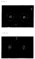
Fig. 1 is a microphotograph at 30 times
magnification in which a solder bump after reflow in
an example 1 of the present invention in an
experimental example 1 of a first embodiment is
photographed;
Fig. 2 is a microphotograph at 30 times
magnification in which a solder bump after reflow in
a comparison example 1 in the experimental example 1
of the first embodiment is photographed;
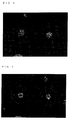
Fig. 3 is a microphotograph at 30 times
magnification in which a solder bump after reflow in
a comparison example 2 in the experimental example 1
of the first embodiment is photographed;
Fig. 4 is a microphotograph at 30 times
magnification in which a solder bump after reflow in
a comparison example 3 in the experimental example 1
of the first embodiment is photographed; and
Fig. 5 is a schematic sectional view showing the
primary structure of a semiconductor device in a
third embodiment.
Detailed Description of the Preferred Embodiments
Hereinafter preferred embodiments in which the
present invention is applied will be explained in
detail.
-First Embodiment-
If the content of Ag is too low, solidus
temperature (melting point) of a solder alloy rises,
and a function as a solder usable at around 220°C is
lost. If the Ag content is 2.0 wt% or higher, the
solder has an appropriate melting point and can be
utilized at around 220°C.
Further, if the content of Ag is 3.0 wt% or
lower, β-dendrites are suppressed from growing after
reflow, which can realize a solder bump having an
excellent surface property without roughness.
When Cu is added to an Sn-Ag solder alloy, the
solidus temperature (melting point) lowers if the Cu
content is 1.5 wt% or lower, while the solidus
temperature abruptly rises if the Cu content exceeds
1.5 wt%. Therefore, in the present invention, an
upper limit of the Cu content is defined as 1.5 wt%.
In the Sn-Ag alloy, networks of Ag3Sn
intermetallic compounds are produced in the
solidification structure, which improves the strength
and a fatigue property of the solder. In the alloy
containing only Sn-Ag, the networks of the Ag3Sn
intermetallic compounds are not sufficiently
connected to each other. However, if 0.3 wt% or more
Cu is added to the Sn-Ag solder alloy, ring-shaped
networks of the Ag3Sn intermetallic compounds therein
become dense and the strength and the fatigue
property of the solder bump are improved, which makes
it possible to ensure the strength and a thermal
fatigue-resistant characteristic demanded by an
electronic part. Therefore, in the present invention,
a lower limit of the Cu content is defined as 0.3 wt%.
As described above, in the present invention, the
composition of the solder alloy containing 2.0 to 3.0
wt% Ag, 0.3 to 1.5 wt% Cu, and the balance Sn and
inevitable impurities is applied as a lead-free
solder alloy so that it becomes possible to obtain
the appropriate melting point and to secure the
excellent thermal fatigue-resistant characteristic as
well as to secure the surface property after the
reflow at the same time. As a result, when this
solder alloy is used for a solder bump of the
electronic member, the evaluation for bump formation
can be made in an optical method.
A solder ball having the above composition is
suitable as a solder ball for forming the solder bump.
Particularly, in a fine solder ball whose diameter is
300 µm or shorter, the evaluation of a solder bump
formed of a solder ball having the conventional
composition is difficult to be made in the optical
method. However, in a case where the solder ball
according to the present invention is used, the
evaluation of the solder bump in the optical method
can be made because its surface property is excellent.
-Experimental Examples-
-Experimental Example 1-
Solder balls having a diameter of 760 µm are
prepared using solder alloys having the composition
shown in Table 1, put on an electrode on a substrate
utilizing adhesion of flux, and heated in a reflow
furnace, and surface properties of solder bumps after
reflow are observed.
Light is irradiated from a light source above the
substrate, the electrode on the substrate is
photographed, and images of light reflected by the
solder bumps are compared. If the image of light
focuses only on a top of the semi-spherical bump, it
is judged as acceptable, while if the image of light
is dispersed all over the electrode, it is judged as
bump formation failure.
(Table 1)
An example 1 of the present invention is a solder
alloy having the composition according to the present
invention, a comparison example 1 is an Sn-Ag solder
alloy, a comparison example 2 is an Sn-Ag-Bi-Cu
solder alloy, and a comparison example 3 is a Pb-Sn
lead solder alloy. Surface properties of solder
bumps after reflow in these examples are photographed
and shown in Fig. 1 to Fig. 4 as photographs enlarged
at 30 times magnification. Fig. 1 corresponds to the
example 1 of the present invention, Fig. 2
corresponds to the comparison example 1, Fig. 3
corresponds to the comparison example 2, and Fig. 4
corresponds to the comparison example 3. In the
example 1 of the present invention and the comparison
example 3 (lead solder), images of light focus only
on tops of the bumps, that is, excellent evaluation
results have been obtained. The reason is that the
surface properties after reflow are excellent. In
the comparison examples 1 and 2, images of light are
dispersed all over the surfaces of the bumps, that is,
unacceptable evaluation results as bumps have been
obtained. The reason is that the surface properties
become rough after reflow and the light is reflected
irregularly.
-Experimental Example 2-
Solder balls having a diameter of 300 µm are
prepared using the same solder alloys having the
component shown in Table 1 as those in the
experimental example 1. With the solder balls,
silicon chip parts and printed boards are flip-chip
connected, and temperature cycle thermal shock tests
are conducted using the flip-chip connected silicon
chip parts and printed boards as specimens.
The silicon chip part has 64 electrode lands,
each of which has a diameter of 200 µm, arranged on a
silicon chip in its circumference with spacing of 0.3
mm therebetween. The printed board is a glass-epoxy
resin substrate having wiring provided on one surface
thereof, and has also electrode lands in positions
corresponding to the electrode lands on the silicon
chip.
First of all, the above-described solder balls
are put on the electrode lands of both of the silicon
chip part and the printed board, and heated in the
reflow furnace where the solder balls are made to
reflow so that solder bumps are formed. Then, the
silicon chip part and printed board having the solder
bumps are made to come into contact with each other
with their solder bumps, heated again in the reflow
furnace where both electrode portions are joined, so
that the silicon chip part and the printed board are
flip-chip connected to be the specimen.
The formed specimen is heated and cooled
repeatedly under the temperature cycle condition of
repeating -40°C (30 minutes) and +125°C (30 minutes).
The tests are conducted with temperature cycle
repeated times (TCT cycle time) ranging from 100
cycles to 900 cycles at 100 cycle intervals, and the
correlation to rupture occurrence ratios of the
solder electrodes is checked.
The evaluation result of the rupture occurrence
ratio (%) at each TCT cycle time is shown in Table 2.
The specimens using the solder alloy in the example 1
of the present invention and the comparison example 1
exhibit low rupture occurrence ratios, that is, they
have excellent thermal fatigue-resistant
characteristics, while the specimen in the comparison
example 3 (lead solder) exhibits a high rupture
occurrence ratio. A fatigue-resistant characteristic
of the specimen in the comparison example 2
deteriorates by approximately 20% because it contains
Bi.
(Table 2)
As explained in the experimental examples 1 and 2,
when the solder alloy having the composition
according to the present invention is used, the
excellent results can be obtained in both terms of
the surface property after reflow and the thermal
fatigue-resistant characteristic.
-Experimental Example 3-
Solder balls having a diameter of 300 µm are
prepared using solder alloys having the composition
shown in Table 3, solder bumps are formed in the same
manner as that in the above experimental example 1,
and surface properties of the solder bumps are
observed. As a result, in the observation of the
surfaces of the solder bumps after reflow, an
extremely excellent surface property in which an
image of light focuses only on a top of the semi-spherical
bump is obtained in each of examples 2 to 4
of the present invention compared with a comparison
example 1 and a comparison example 2.
(Table 3)
-Second Embodiment-
If the content of Ag is too low, the solidus
temperature (melting point) of a solder alloy rises,
and a function as a solder usable at around 220°C is
lost. If the Ag content is 2.0 wt% or higher, the
solder alloy has an appropriate melting point and can
be utilized at around 220°C. Further, if the Ag
content is 3.0 wt% or lower, β-dendrites are
suppressed from growing after reflow, which can
realize a solder bump having an excellent surface
property without roughness. The Ag content is more
preferably 3.0 wt% or lower.
When Cu is added to an Sn-Ag solder alloy, the
solidus temperature (melting point) lowers if the Cu
content is 1.5 wt% or lower, while the solidus
temperature abruptly rises if the Cu content exceeds
1.5 wt%. Therefore, in the present invention, an
upper limit of the Cu content is defined as 1.5 wt%.
In the Sn-Ag alloy, networks of Ag3Sn
intermetallic compounds are produced in the
solidification structure, which improves the strength
and a fatigue property of the solder. In the alloy
containing only Sn-Ag, the networks of the Ag3Sn
intermetallic compounds are not sufficiently
connected to each other. However, if 0.3 wt% or more
Cu is added to the Sn-Ag solder alloy, ring-shaped
networks of the Ag3Sn intermetallic compounds therein
become dense and the strength and the fatigue
property of the solder bump are improved, which makes
it possible to ensure the strength and a thermal
fatigue-resistant characteristic demanded by an
electronic part. Therefore, in the present invention,
a lower limit of the Cu content is defined as 0.3 wt%.
A lower limit of the content of Bi is defined as
0.05 wt% because, if the Bi content is less than 0.05
wt%, an effect of lowering the melting point is not
sufficient. Further, if the Bi content increases,
the mechanical strength of the solder alloy increases
while the ductility of the solder alloy decreases.
Moreover, it has been found that, if the Bi content
is too high, needle-shaped Bi crystals precipitate on
a surface of the solder after reflow, which
deteriorates the surface property. If the Bi content
is 1.5 wt% or lower, the ductility of the solider
alloy is excellent as well as the surface property of
the solder after reflow is also excellent. Therefore,
an upper limit of the Bi content is defined as 1.5
wt%. The Bi content is preferably 1.0 wt% or lower.
A lower limit of the content of Sb is defined as
0.2 wt% because an effect of suppressing Sn from
transforming at low temperature is insufficient if
the Sb content is lower than 0.2 wt%. An upper limit
of the Sb content is defined as 1.5 wt% because, if
the Sb content exceeds 1.5 wt%, the surface roughness
of the solder after reflow cannot be suppressed and
an effect of improving the thermal fatigue-resistant
characteristic also decreases.
If the total content of Ag, Cu, Sub, and Bi
exceeds 5.0 wt%, the surface after reflow becomes
rough because of precipitation, oxidization, and the
like of alloy elements on a ball surface and the
excellent surface property cannot be obtained.
Accordingly, an upper limit of the total content of
Ag, Cu, Sb, and Bi is defined as 5.0 wt%.
As described above, in the present invention, the
composition of the solder alloy containing 2.0 to 3.0
wt% Ag, 0.3 to 1.5 wt% Cu, 0.05 to 1.5 wt% Bi, 0.2
to 1.5 wt% Sb, and the balance Sn and inevitable
impurities, in which the total content of Ag, Cu, Sb,
and Bi is 5.0 wt% or lower, is applied as a lead-free
solder alloy, so that it becomes possible to obtain
the appropriate melting point and to greatly improve
the thermal fatigue-resistant characteristic as well
as to secure the surface property after reflow at the
same time. Consequently, when this solder alloy is
used for the solder bump of the electronic member,
the evaluation for bump formation can be made in the
optical method. Further, even when the electronic
member using the solder alloy is used in cold
climates, sufficient thermal fatigue-resistant
characteristic can be obtained.
A solder ball having the above-described
composition is suitable as a solder ball for forming
the solder bump. Particularly, in a fine solder ball
whose diameter is 300 µm or shorter, the evaluation
of a solder bump formed of a solder ball having the
conventional composition is difficult to be made in
the optical method. However, in a case where the
solder ball according to the present invention is
used, the evaluation of the solder bump in the
optical method can be made because the surface
property of the solder bump after reflow is smooth
and excellent.
-Experimental Examples-
-Experimental Example 1-
Solder balls having a diameter of 300 µm are
prepared using solder alloys having the composition
shown in Table 4, put on an electrode on a substrate
utilizing adhesion of flux, and heated in a reflow
furnace, and the surface properties of solder bumps
after reflow are observed.
Light is irradiated from a light source above the
substrate, the electrode on the substrate is
photographed, and images of light reflected by the
solder bump are compared. If the image of light
focuses only on a top of the semi-spherical bump, it
is judged as acceptable, while if the image of light
is dispersed all over the electrode, it is judged as
bump formation failure.
(Table 4)
Examples 1 to 4 of the present invention are
solder alloys having the composition according to the
present invention, a comparison example 1 is a solder
alloy in which the total content of Ag, Cu, Sb, and
Bi exceeds 5.0 wt%, a comparison example 2 is a
solder alloy in which Sb exceeds the upper limit of
the present invention and Bi is not contained, a
comparison example 3 is an Sn-Ag solder alloy, a
comparison example 4 is an Sn-Ag-Bi-Cu solder alloy,
and a comparison example 5 is a Pb-Sn lead solder
alloy. A surface property of the solder bump after
reflow in each of the examples is photographed and
the surface luster is evaluated. In the examples 1
to 4 of the present invention and the comparison
example 5 (lead solder), images of light focus only
on tops of the bumps, that is, excellent evaluation
results have been obtained. The reason is that the
surface properties after reflow are excellent. In
the comparison examples 1 to 4, images of light are
dispersed all over the surfaces of the bumps, that is,
unacceptable evaluation results as bumps have been
obtained. The reason is that the surface properties
become rough after reflow and the light is reflected
irregularly.
-Experimental Example 2-
Solder balls having a diameter of 300 µm are
prepared using the same solder alloys having the
component shown in Table 4 as those in the
experimental example 1. With the solder balls,
silicon chip parts and printed boards are flip-chip
connected, and temperature cycle thermal shock tests
are conducted using the flip-chip connected silicon
chip parts and printed boards as specimens.
The silicon chip part has 64 electrode lands,
each of which has a diameter of 200 µm, arranged on a
silicon chip in its circumference with spacing of 0.3
mm therebetween. The printed board is a glass-epoxy
resin substrate having wiring provided on one surface
thereof, and has also electrode lands in positions
corresponding to the electrode lands on the silicon
chip.
First of all, the above-described solder balls
are put on the electrode lands of both of the silicon
chip part and the printed board, and heated in the
reflow furnace where the solder balls are made to
reflow so that solder bumps are formed. Then, the
silicon chip part and printed board having the solder
bumps are made to come into contact with each other
with their solder bumps, heated again in the reflow
furnace where both electrode portions are joined, so
that the silicon chip part and the printed board are
flip-chip connected to be the specimen.
The formed specimen is heated and cooled
repeatedly under the temperature cycle condition
where -40°C (30 minutes) and +125°C (30 minutes) are
repeated. The tests are conducted with temperature
cycle repeated times (TCT cycle time) ranging from
100 cycles to 1100 cycles at 100 cycle intervals, and
the correlation to rupture occurrence ratios of the
solder electrodes is checked.
The evaluation result of the rupture occurrence
ratio (%) at each TCT cycle time is shown in Table 5.
It is obvious that the specimens using the solder
alloys in the examples 1 to 4 of the present
invention exhibit extremely low rupture occurrence
ratios and are particularly excellent in thermal
fatigue-resistant characteristic. The thermal
fatigue-resistant characteristics in the comparison
example 2 (Sb exceeding the upper limit) and the
comparison example 3 (Sn-Ag) are approximately equal
to those in the examples of the present invention.
In the comparison example 1 and comparison example 4
(Sn-Ag-Cu-Bi), the thermal fatigue-resistant
characteristics are reasonably excellent but the
rupture occurrence ratios are high compared with the
examples of the present invention. The comparison
example 5 (lead solder) exhibits a high rupture
occurrence ratio.
(Table 5)
As explained in the experimental examples 1 and 2,
when the solder alloy having the composition
according to the present invention is used, the
excellent result can be obtained in both terms of the
surface property after reflow and the thermal
fatigue-resistant characteristic.
-Third Embodiment-
In this embodiment, an electronic member such as
a semiconductor device having the solder bump
disclosed in the first or second embodiment is
explained as an example.
Fig. 5 is a schematic sectional view showing the
primary structure of the semiconductor device of the
embodiment.
This semiconductor device has the structure in
which electrodes 2 of a semiconductor chip 1 and
inner leads 3 are joined with solder bumps 4 formed
of the lead-free solder alloy disclosed in the first
or second embodiment and are molded by resin 5. In
the semiconductor device, the solder bumps 4 are
joined to the electrodes 2 arranged in a
circumference of the semiconductor chip 1 in advance,
or are joined to the inner leads 3 in advance, and
the semiconductor chip 1 and the inner leads 3 are
put together and joined by one operation.
According to the embodiment, in preparing the
semiconductor device (electronic member), the quality
of the solder bumps can be properly evaluated even if
a large number of fine solder bumps are formed, and
therefore the electronic member having excellent
quality can be obtained. Particularly, in a case of
a fine solder bump having a side length of 0.2 mm or
shorter, an excellent result which cannot be realized
by the solder bump having the conventional
composition can be obtained. The electronic member
in which plural electronic parts are joined with the
solder electrodes having the above composition has
excellent characteristics that it has the solder
electrodes of excellent quality because the quality
is properly evaluated in a preparation step, and
further that the solder electrodes has a suitable
thermal fatigue-resistant characteristic.
Industrial Applicability
By using the solder alloy having the composition
according to the present invention, the surface
property of the solder bump after reflow becomes
excellent, which makes it possible to properly judge
the quality of the bump formation in the optical
method. At the same time, the suitable melting point
can be obtained and the excellent thermal fatigue-resistant
characteristic can be realized. The solder
bump can be formed using the solder ball having the
composition of the present invention.
Further, the electronic member, in which the
solder bump having the composition of the present
invention is formed, and the electronic member, in
which the electronic parts are joined with the solder
electrode having the composition of the present
invention, have advantages that the electrodes of
high quality are formed therein without including
failures and that the thermal fatigue-resistant
characteristics of the electrodes are excellent.
In addition, although the solder alloy of the
present invention contains 2.0 to 3.0 wt% Ag added
thereto, that is, the Ag content is lower than that
of the conventional solder alloy which contains
similar components, joint reliability equal to that
of the conventional solder alloy can be achieved so
that an economic advantage that the excellent
property is realized at a low cost is also brought
about.
| | SOLDER ALLOY COMPOSITION (wt%) |
| | Sn | Ag | Cu | Bi | Pb |
| EXAMPLE 1 OF THE PRESENT INVENTION | BALANCE | 2.6 | 0.6 |
| COMPARISON EXAMPLE 1 | BALANCE | 3.5 |
| COMPARISON EXAMPLE 2 | BALANCE | 3.3 | 0.5 | 1.0 |
| COMPARISON EXAMPLE 3 | 63 | | | | BALANCE |
| | RUPTURE OCCURRENCE RATIO (%) |
| TCT CYCLE TIME | 100 CYCLES | 200 CYCLES | 300 CYCLES | 400 CYCLES | 500 CYCLES | 600 CYCLES | 700 CYCLES | 800 CYCLES | 900 CYCLES |
| EXAMPLE 1 OF THE PRESENT INVENTION | 0 | 0 | 4.7 | 20.3 | 46.9 | 84.8 | 88.2 | 98.7 | 100 |
| COMPARISON EXAMPLE 1 | 0 | 0 | 7.8 | 18.7 | 53.1 | 71.9 | 89.1 | 96.9 | 100 |
| COMPARISON EXAMPLE 2 | 0 | 2.0 | 7.8 | 28.1 | 82.8 | 96.9 | 100 | 100 | 100 |
| COMPARISON EXAMPLE 3 | 0 | 7.8 | 46.9 | 95.3 | 100 | 100 | 100 | 100 | 100 |
| | SOLDER ALLOY COMPOSITION (wt%) |
| | Sn | Ag | Cu | Bi |
| EXAMPLE 2 OF THE PRESENT INVENTION | BALANCE | 2.0 | 0.3 |
| EXAMPLE 3 OF THE PRESENT INVENTION | BALANCE | 2.5 | 0.6 |
| EXAMPLE 4 OF THE PRESENT INVENTION | BALANCE | 3.0 | 1.5 |
| COMPARISON EXAMPLE 1 | BALANCE | 3.5 |
| COMPARISON EXAMPLE 2 | BALANCE | 3.3 | 0.5 | 1.0 |
| SOLDER ALLOY COMPOSITION (wt%) |
| EXAMPLE / ELEMENT | Sn | Ag | Cu | Bi | Sb | Pb | SURFACE LUSTER |
| EXAMPLE 1 OF THE PRESENT INVENTION | BALANCE | 2.6 | 0.6 | 0.1 | 0.5 | | ○ |
| EXAMPLE 2 OF THE PRESENT INVENTION | BALANCE | 2.6 | 0.6 | 1.0 | 0.5 | | ○ |
| EXAMPLE 3 OF THE PRESENT INVENTION | BALANCE | 2.6 | 0.6 | 0.5 | 0.5 | | ○ |
| EXAMPLE 4 OF THE PRESENT INVENTION | BALANCE | 2.6 | 0.5 | 0.5 | 1.0 | | ○ |
| COMPARISON EXAMPLE 1 | BALANCE | 2.6 | 0.6 | 1.5 | 0.5 | | × |
| COMPARISON EXAMPLE 2 | BALANCE | 2.6 | 0.6 | | 3.0 | | × |
| COMPARISON EXAMPLE 3 | BALANCE | 3.5 | | | | | × |
| COMPARISON EXAMPLE 4 | BALANCE | 3.5 | 0.5 | 1.0 | | | × |
| COMPARISON EXAMPLE 5 | 63 | | | | | BALANCE | ○ |
| RUPTURE OCCURRENCE RATIO (%) |
| TCT CYCLE TIME | 100 CYCLES | 200 CYCLES | 300 CYCLES | 400 CYCLES | 500 CYCLES | 600 CYCLES | 700 CYCLES | 800 CYCLES | 900 CYCLES | 1000 CYCLES | 1100 CYCLES |
| EXAMPLE 1 OF THE PRESENT INVENTION | 0 | 0 | 0 | 5.2 | 19.3 | 41.3 | 78.8 | 83.0 | 91.6 | 97.4 | 100 |
| EXAMPLE 2 OF THE PRESENT INVENTION | 0 | 0 | 0 | 6.2 | 22.2 | 47.1 | 89.1 | 91.0 | 99.7 | 100 | 100 |
| EXAMPLE 3 OF THE PRESENT INVENTION | 0 | 0 | 0 | 5.2 | 24.3 | 42.3 | 82.8 | 88.0 | 95.6 | 100 | 100 |
| EXAMPLE 4 OF THE PRESENT INVENTION | 0 | 0 | 0 | 3.2 | 12.3 | 38.9 | 57.6 | 69.6 | 82.7 | 92.7 | 100 |
| COMPARISON EXAMPLE 1 | 0 | 0 | 4.6 | 20.3 | 46.9 | 84.8 | 88.3 | 98.6 | 100 | 100 | 100 |
| COMPARISON EXAMPLE 2 | 0 | 0 | 0 | 7.2 | 14.9 | 33.1 | 57.9 | 76.2 | 88.2 | 98.1 | 100 |
| COMPARISON EXAMPLE 3 | 0 | 0 | 0 | 4.2 | 17.3 | 40.9 | 75.3 | 90.1 | 97.3 | 100 | 100 |
| COMPARISON EXAMPLE 4 | 0 | 0 | 0 | 12.3 | 34.9 | 67.3 | 88.1 | 93.7 | 100 | 100 | 100 |
| COMPARISON EXAMPLE 5 | 0 | 7.6 | 46.8 | 95.4 | 100 | 100 | 100 | 100 | 100 | 100 | 100 |