EP1248373A1 - Apparatus for and method of generating a clock from an available clock of arbitrary frequency - Google Patents
Apparatus for and method of generating a clock from an available clock of arbitrary frequency Download PDFInfo
- Publication number
- EP1248373A1 EP1248373A1 EP20010201261 EP01201261A EP1248373A1 EP 1248373 A1 EP1248373 A1 EP 1248373A1 EP 20010201261 EP20010201261 EP 20010201261 EP 01201261 A EP01201261 A EP 01201261A EP 1248373 A1 EP1248373 A1 EP 1248373A1
- Authority
- EP
- European Patent Office
- Prior art keywords
- frequency
- clock
- cycles
- standby
- available
- Prior art date
- Legal status (The legal status is an assumption and is not a legal conclusion. Google has not performed a legal analysis and makes no representation as to the accuracy of the status listed.)
- Granted
Links
Images



Classifications
-
- H—ELECTRICITY
- H03—ELECTRONIC CIRCUITRY
- H03L—AUTOMATIC CONTROL, STARTING, SYNCHRONISATION OR STABILISATION OF GENERATORS OF ELECTRONIC OSCILLATIONS OR PULSES
- H03L7/00—Automatic control of frequency or phase; Synchronisation
Definitions
- the present invention relates generally to clock generator circuits and more particularly relates to an apparatus for and method of generating an accurate clock from an available clock source having an arbitrary frequency.
- an active or normal operating mode operates in one of two modes: an active or normal operating mode and a reduced power standby mode.
- the active mode is used for normal operation of the device while standby mode is used when one or more portions of the device are not needed.
- standby mode is used when one or more portions of the device are not needed.
- the phone is in normal active mode.
- standby mode typically uses far less power than active mode.
- the device While in standby mode (or sleep mode as it is commonly referred to), the device may 'wake up' periodically to maintain synchronization with the base station or other central device either via an interrupt mechanism, an internal state machine, or other means. Thus, during standby times, the phone may temporarily not communicate with the network but it still maintains synchronization with it. In such a mode, the power consumption of the device is greatly reduced, which is especially crucial in devices that are battery powered.
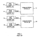
- FIG. 1 A block diagram illustrating a prior art device comprising two communication systems wherein each individual communication system has its own fast clock and standby clock sources is shown in Figure 1.
- Communication system #1 12 operates in either active mode or standby mode. Each mode requires a different clock frequency.
- a fast clock source #1 10 is used to generate a fast clock having a frequency f FAST1 while a second slow clock source #1 14 is used to generate a standby clock (i.e., slow clock) having a frequency f STDBY1 .
- communication system #2 20 operates in either active mode or standby mode. Each mode requires a different clock frequency.
- a fast clock source #2 16 is used to generate a fast clock having a frequency f FAST2 while a second slow clock source #2 18 is used to generate a standby clock (i.e., slow clock) having a frequency f STDBY2 .
- a faster frequency source is used when the device is active (with increased current consumption) and a slower frequency source is used when the device is in standby.
- the slow frequency source must be chosen such that the proper timing corresponding to network time instances (i.e., events or occurrences) can be derived from it.
- a slower frequency source i.e., clock source #1 14
- clock source #1 14 already exists which is appropriate for deriving the clock timing needed for standby mode.
- a second slow clock source is required since the already existing slow clock source #1 is likely not appropriate and would lead to incorrect turn-on times (i.e., either too early or too late) when returning from sleep or standby mode to active mode in communication system #2. Turn on times that are too early result in increased power consumption and consequently shorter battery life. Turn on times that are too late may cause the system to lose synchronization with the network,
- the present invention is an apparatus for and method of generating a clock signal having a desired frequency that is derived from a clock source having any arbitrary frequency.
- the mechanism described herein When utilized to supply the slow clock for the standby mode of operation of a device, the mechanism described herein enables the use of an arbitrarily low frequency source while providing accurate timing. This results in reduced power consumption that would otherwise be wasted during unnecessary time spent in the active mode of operation.
- the mechanism of the present invention generates an average rate, very close to the optimal rate desired, by 'swallowing' or absorbing clock cycles of the available frequency source.
- precise timing is achieved by adding correcting time intervals, which are based on counting pulses from the higher rate clock source.
- a clock frequency generator functions to generate the standby clock from the available frequency source.
- the clock frequency generator comprises a standby mode state machine and a jitter calculation processor. Timing calculations are performed by the jitter calculation processor and the standby mode state machine functions to generate the desired standby mode clock frequency.
- the state machine utilizes counters to track the number of cycles of the available clock and the number of generated cycles of the standby clock.
- the processor is aware of the state of the counters in the state machine that is typically implemented in hardware.
- the jitter calculation processor determines the accumulated jitter error (i.e., the interval of time to be compensated) in accordance with (1) the accumulated timing error due to the difference in frequencies between the available and desired clock frequencies and (2) the number of clock cycles absorbed or swallowed.
- This interval is measured using the fast clock rate which is to be activated at the proper time when switching back to active mode from standby mode. Only when the last portion of the interval is measured, can the device be permitted to re-enter the active mode by powering the active mode circuitry in the device. This minimizes the average power consumption of the device.
- the mechanism of the present invention can utilize any available frequency source in generating the standby frequency. This permits better system integration (i.e., reduced size, lower cost, etc.) since additional frequency sources are not required.
- the application of the clock generator apparatus and method of the present invention to communication systems is intended to provide the benefit of reduced costs.
- the invention is intended to reduce costs in devices where a second communication system (e.g., a communication systems conforming to the Bluethooth standard) is added to an already existing one (e.g., a GSM cellular telephone handset) and it is desired to any additional required power consumption to a minimum.
- a second communication system e.g., a communication systems conforming to the Bluethooth standard
- an already existing one e.g., a GSM cellular telephone handset
- a method of generating a first clock signal having a desired first frequency from an available second clock signal having a second frequency wherein the second frequency is higher than the first frequency comprising the steps of generating the first clock signal by sequencing through a predetermined number of states whereby during each state a first plurality of cycles of the second clock are absorbed and a second plurality of cycles of the second clock are output as cycles of the first clock, correcting timing differences between the desired first frequency and the available second frequency at the end of each the sequence by adding a correcting time interval to the first clock such that the average frequency of the first clock is substantially equal to the desired first frequency and calculating a compensation interval to compensate for the accumulated timing jitter of the first clock signal during a specified time interval.
- a method of generating a first clock signal having a desired first frequency from a second clock signal having a second frequency comprising the steps of counting a first predetermined number of cycles of the second clock signal on a periodic basis, outputting a second predetermined number of cycles of the second clock signal on a periodic basis and correcting accumulated timing differences between the desired first frequency and the second frequency by counting a third predetermined number of cycles of the second clock signal and outputting a fourth predetermined number of cycles of the second clock signal such that the average frequency of the first clock is substantially equal to the desired first frequency.
- a method of accurately timing the period of time the device is in the standby mode wherein the device utilizes a standby clock having a desired first frequency generated from an available clock having a second frequency while in standby mode and utilizes a fast clock having a third frequency while in the active mode, the method comprising the steps of dividing the output of the available clock into continuously repeating sequence of states, for all states but the last in the sequence: counting a first predetermined number of cycles of the available clock signal, outputting as the standby clock a second predetermined number of cycles of the available clock signal, for the last state in the sequence: correcting timing differences accumulated during the current sequence between the desired first frequency and the second frequency by counting a third predetermined number of cycles of the available clock signal and outputting as the standby clock a fourth predetermined number of cycles of the available clock signal such that the average frequency of the standby clock is substantially equal to the desired first frequency and calculating a compensation interval to
- an apparatus for generating a standby clock frequency in a device having an active and a standby mode of operation wherein the device utilizes the standby clock having a desired first frequency while in standby mode and utilizes a fast clock having a second frequency while in the active mode
- the apparatus comprising means for generating the standby clock from an available clock source comprising means for absorbing a first plurality of cycles of the available clock, means for outputting as the standby clock a second plurality of cycles of the available clock, adjustment means for periodically adjusting for the accumulated timing error caused by the differences in frequencies of the standby clock and the available clock such that the average frequency of the standby clock is substantially equal to the desired first frequency and means for calculating a compensation interval to compensate for the timing error of the standby clock signal accumulated during the time the device was in standby mode, the compensation interval derived from a jitter value determined in accordance with the total number of cycles of the available clock counted and the total number of cycles of the available clock generated during the current
- an apparatus for generating a standby clock frequency in a device having an active and a standby mode of operation wherein the device utilizes the standby clock having a desired first frequency while in standby mode and utilizes a fast clock having a second frequency while in the active mode
- the apparatus comprising a clock frequency generator adapted to generate the standby clock from an available clock source, the clock frequency generator comprising a standby mode state machine operative to: absorb a first plurality of cycles of the available clock, output as the standby clock a second plurality of cycles of the available clock, periodically adjust for the accumulated timing error caused by the differences in frequencies of the standby clock and the available clock such that the average frequency of the standby clock is substantially equal to the desired first frequency and a jitter calculator adapted to calculate a compensation interval to compensate for the timing error of the standby clock signal accumulated during the time the device was in standby mode, the compensation interval derived from a jitter value determined in accordance with the total number of cycles of the available clock
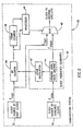
- FIG. 2 A block diagram illustrating the clock frequency generator of the present invention operative in an example communication system is shown in Figure 2.
- the communication system generally referenced 30, comprises two clock sources: clock source #1 32 which provides the frequency source f FAST for the fast clock and clock source #2 34 which provides the frequency source f AVAIL for the slow clock (i.e., standby mode clock).
- clock source #2 comprises the available clock source and may have any arbitrary frequency. It is typically derived from a clock source having a frequency other than the desired frequency that is used elsewhere in the system.
- the fast clock is input to a bit counter 36 that in turn feeds a frame counter 38.
- the bit and frame counters are used during active mode to provide timing for bit and frame boundaries.
- data is sent organized as a hierarchy of data units, e.g., bits, frames, superframes, etc.
- the bit counter functions to define the bit number within a frame while the frame counter functions to count frames.
- the contents of the bit counter can be set by loading in a new count value.
- the output of both the bit and frame counters are input to a processor 46 that functions to control the operation of the communication system 30.
- the available clock is input the clock frequency generator 40 which comprises a standby mode state machine 44 and a jitter calculation processor 42.
- the clock frequency generator 40 is used during standby mode to generate the standby clock having the desired standby frequency f STDBY .
- the standby clock signal output of the standby mode state machine 44 and the output of the fast clock source 32 are input to a multiplexor 48.
- the mux select is controlled by the processor 46.
- the output of the mux is used by the internal circuitry of the communication system 30. When the system 30 is in active mode, the mux is configured to output the fast clock. When the system is in standby mode, the mux is configured to output the standby clock.
- the processor is suitably programmed to control the mux so as to maintain synchronization with the network regardless of which mode the communication system 30 is in.
- FIG. 3 A diagram illustrating the timing of the switching between the active and standby modes is shown in Figure 3. Note that the ticks along the timeline indicate frames.
- T 1 which is typically determined in accordance with the communications protocol in use, the system receives a command or internally decides to switch from the active mode to standby mode. While in standby mode, the system uses the standby clock for internal operations and typically consumes far less power.
- the system decides to switch back to the active mode.
- the system switches from the slower standby clock back to the fast active clock slightly before the device goes into the active mode.
- the state of the clock frequency generator is preserved at time T 1 and T 2 , as indicated by state and state", respectively. Note that in accordance with the communication protocol, the system only switches between active and standby modes on a frame boundary.
- the standby mode state machine 44 functions to generate the standby clock having the desired frequency using the available clock (i.e., clock source #2) as the frequency source.
- the available clock may have any arbitrary frequency since the clock frequency generator performs the necessary conversions of clock rate while compensating for errors caused by jitter.
- the standby mode state machine 44 comprises circuitry (i.e., counters, registers, etc.) to generate the standby clock.
- the state machine comprises a plurality of states wherein in each state, a certain number of standby clock cycles are generated on a periodic basis in accordance with the available clock. This is illustrated in Figure 4 which shows a timing diagram illustrating the standby clock generated by the clock frequency generator of the present invention utilizing an available clock having arbitrary frequency.
- the available clock is shown segmented over time into a plurality of states. States #N and #N+1 are shown to illustrate this principle.
- the state machine is operative to count available clock cycles while generating a particular number of standby clock cycles. Each cycle of the standby clock has a period T STDBY equal to 1 / ⁇ AVAIL . In order to generate a clock having an average frequency equal to the desired standby clock rate, one or more cycles of the available clock arc absorbed or 'swallowed'.
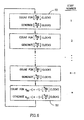
- FIG. 5 A diagram illustrating the timing of the switching between active and standby modes in relation to the timing of the standby mode state machine is shown in Figure 5.
- the timeline shown is for one complete cycle of the state machine.
- a full cycle is defined to have ⁇ states.
- the state machine is adapted to be free running and is driven by the available clock source.
- the state machine cycles through states #1 through # ⁇ and then returns to state #1.
- states #1 through # ⁇ -1 the same number of standby clock cycles are generated. Any needed clock compensation is done in the last state # ⁇ .
- the standby clock cycles generated when taken together as an average, effectively generate the exact desired standby clock frequency.
- the number of standby clocks generated up to that point may not, however, combine to effectively generate the exact desired standby clock frequency.
- the jitter error accumulated up to that point has not yet been compensated for. As described above, compensation for jitter accumulated during states #1 through # ⁇ -1 is compensated for in the last state # ⁇ .
- the switch points time T 1 and T 2 may occur at any time during the state machine cycle.
- the jitter accumulated during the time the system was in the standby state i.e., the time interval from T 1 to T 2
- this time interval typically spans many cycles of the state machine but since the jitter is compensated for completely at the end of each cycle, only the jitter accumulated during the first and the last cycles need be compensated for. This corresponds to the cycles during which the two switching events occurred.
- a state transition diagram of the standby mode state machine is shown in Figure 6.
- the entity F SB is defined as the desired standby clock frequency and F AV is defined as the available clock frequency.
- the term GCD is defined as the greatest integer common divisor between F SB and F AV .
- the integer values N SB and N AV are then calculated by dividing by GCD as shown below in Equations 1 and 2.
- N AV F AV GCD
- N AV represents the total number of clock cycles of the available clock in one full cycle of the state machine.
- N SB represents the desired number of clock cycles of the standby clock in one full state machine cycle.
- the value ⁇ is defined as the rounded ratio of N AV to N SB As described hereinabove, the temporary jitter produced when generating F SB from F AV is compensated for at the end of the state machine cycle.
- the state machine is operative to generate the standby clock so as to reduce the jitter to a minimum.
- the state machine is adapted to comprise ⁇ states. For states numbered #1 through # ⁇ -1 (referenced 50) the machinc counts clock cycles of the available clock and generates clock cycles of the standby clock. During the last state #a (referenced 52) the machine counts clock cycles and generates clock cycles.
- N AV , N SB and hence a are known a priori and are precalculated. If the state machine is implemented in hardware these values can be easily fixed in the hardware.
- the state machine uses a first counter I to track the state number and a second counter cycle_count to count between 1 and when the state is in the range 1 to ⁇ -1 and between I and when in the ⁇ state.
- the combination of I and cycle_count counters represent the current status of standby clock generation.
- the values of both counters are stored. This corresponds to time T; and the values arc designated I' and cycle_count' , and represent state' as shown in Figure 3.
- the values of both counters are stored. This corresponds to time T 2 as shown in Figure 3.
- the amount of jitter generated can be determined. This jitter error can be compensated for at the time of switching back to active mode by adjusting the fast clock counter (i.e., the bit counter).
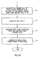
- FIG. 7A and 7B A flow diagram illustrating the jitter correction method of the present invention is shown in Figures 7A and 7B.
- the processor configures the select control input to the multiplexer 48 ( Figure 2) to select the standby clock.
- the jitter calculation processor 42 reads the current state' of the state machine (i.e., the current state number I ' and number of clocks generated cycle_count' both corresponding to time T 1 ) (step 62).
- the processor 42 then calculates the number of cycles of the available clock source that elapsed from the start of the current state machine cycle up to time T 1 (switching from active to standby mode) in accordance with Equation 6 below (step 64).
- the processor then calculates the number of cycles of the available clock source that elapsed from the start of the current state machine cycle up to time T 2 in accordance with Equation 7 below (switching from standby to active mode) (step 66).
- N " AV ( N ' AV + N FR ⁇ N CL )mod N AV where N FR represents the number of frames counted while in standby mode and N CL represents the number of clock cycles in each frame.
- F FAST represents the frequency of the fast clock
- the current_count_value represents the value the fast counter would normally have been set to without the present invention.
- the fast counter would be initialized to zero wherein the counter would be initialized with a negative number or the equivalent number modulo the maximum count value (i.e., the number of bits in a frame).
- the original counter value may be maintained but a portion of the bits of the current frame equal to the jitter error is discarded.
- the communication system may be caused to 'wake-up' earlier (or later) to account for the time represented by the jitter error in order not to lose any bits in a frame. The decision to switch back to the active state is then made and the new_count_value is loaded into the fast counter(step 76).
- N' AV and N" AV can be determined using Equations 6 and 7.
- Equation 10 evaluates to TRUE
- Equation 8 is used to calculate N' SB .
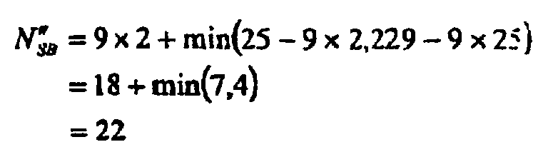
- Equation 13 evaluates to FALSE, thus Equation 12 is used to calculate N" SB .
- the jitter J is calculated in accordance with Equation 16 as shown below
- the new count value is given in accordance with Equation 18 as shown below
- the counter is loaded with -225 or as an equivalent is loaded with 775 assuming 1000 bits (or fast clock cycles) per frame. The clock jitter can thus be compensated for by initializing the bit counter to 775.
Landscapes
- Stabilization Of Oscillater, Synchronisation, Frequency Synthesizers (AREA)
- Synchronisation In Digital Transmission Systems (AREA)
- Electronic Switches (AREA)
Abstract
Description
- The present invention relates generally to clock generator circuits and more particularly relates to an apparatus for and method of generating an accurate clock from an available clock source having an arbitrary frequency.
- Many communication systems such as portable or mobile systems operate in one of two modes: an active or normal operating mode and a reduced power standby mode. The active mode is used for normal operation of the device while standby mode is used when one or more portions of the device are not needed. For example, in a cellular telephone, when a call is received and a conversation is taking place, the phone is in normal active mode. During idle period, however, when the phone is not in use most of the circuitry can be placed in standby mode which typically uses far less power than active mode.
- While in standby mode (or sleep mode as it is commonly referred to), the device may 'wake up' periodically to maintain synchronization with the base station or other central device either via an interrupt mechanism, an internal state machine, or other means. Thus, during standby times, the phone may temporarily not communicate with the network but it still maintains synchronization with it. In such a mode, the power consumption of the device is greatly reduced, which is especially crucial in devices that are battery powered.
- The use of dual modes of operation, i.e., normal active mode and low power standby mode typically requires the use of two different clock frequency sources. A block diagram illustrating a prior art device comprising two communication systems wherein each individual communication system has its own fast clock and standby clock sources is shown in Figure 1.
Communication system # 1 12 operates in either active mode or standby mode. Each mode requires a different clock frequency. A fastclock source # 1 10 is used to generate a fast clock having a frequency fFAST1 while a second slowclock source # 1 14 is used to generate a standby clock (i.e., slow clock) having a frequency fSTDBY1. Similarly,communication system # 2 20 operates in either active mode or standby mode. Each mode requires a different clock frequency. A fastclock source # 2 16 is used to generate a fast clock having a frequency fFAST2 while a second slowclock source # 2 18 is used to generate a standby clock (i.e., slow clock) having a frequency fSTDBY2. - In both systems, a faster frequency source is used when the device is active (with increased current consumption) and a slower frequency source is used when the device is in standby. The slow frequency source, however, must be chosen such that the proper timing corresponding to network time instances (i.e., events or occurrences) can be derived from it.
- A problem arises when a communications module is to be added onto an existing one, as shown in the example whereby
communication system # 2 is added onto already existingcommunication systems # 1. A slower frequency source (i.e.,clock source # 1 14) already exists which is appropriate for deriving the clock timing needed for standby mode. Whencommunications system # 2 is added, a second slow clock source is required since the already existing slowclock source # 1 is likely not appropriate and would lead to incorrect turn-on times (i.e., either too early or too late) when returning from sleep or standby mode to active mode incommunication system # 2. Turn on times that are too early result in increased power consumption and consequently shorter battery life. Turn on times that are too late may cause the system to lose synchronization with the network, - The present invention is an apparatus for and method of generating a clock signal having a desired frequency that is derived from a clock source having any arbitrary frequency. When utilized to supply the slow clock for the standby mode of operation of a device, the mechanism described herein enables the use of an arbitrarily low frequency source while providing accurate timing. This results in reduced power consumption that would otherwise be wasted during unnecessary time spent in the active mode of operation. The mechanism of the present invention generates an average rate, very close to the optimal rate desired, by 'swallowing' or absorbing clock cycles of the available frequency source. In addition, precise timing is achieved by adding correcting time intervals, which are based on counting pulses from the higher rate clock source.
- A clock frequency generator functions to generate the standby clock from the available frequency source. The clock frequency generator comprises a standby mode state machine and a jitter calculation processor. Timing calculations are performed by the jitter calculation processor and the standby mode state machine functions to generate the desired standby mode clock frequency. The state machine utilizes counters to track the number of cycles of the available clock and the number of generated cycles of the standby clock. The processor is aware of the state of the counters in the state machine that is typically implemented in hardware.
- The jitter calculation processor determines the accumulated jitter error (i.e., the interval of time to be compensated) in accordance with (1) the accumulated timing error due to the difference in frequencies between the available and desired clock frequencies and (2) the number of clock cycles absorbed or swallowed. This interval is measured using the fast clock rate which is to be activated at the proper time when switching back to active mode from standby mode. Only when the last portion of the interval is measured, can the device be permitted to re-enter the active mode by powering the active mode circuitry in the device. This minimizes the average power consumption of the device. It is important to note that the mechanism of the present invention can utilize any available frequency source in generating the standby frequency. This permits better system integration (i.e., reduced size, lower cost, etc.) since additional frequency sources are not required.
- The application of the clock generator apparatus and method of the present invention to communication systems is intended to provide the benefit of reduced costs. In particular, the invention is intended to reduce costs in devices where a second communication system (e.g., a communication systems conforming to the Bluethooth standard) is added to an already existing one (e.g., a GSM cellular telephone handset) and it is desired to any additional required power consumption to a minimum.
- There is thus provided in accordance with the present invention a method of generating a first clock signal having a desired first frequency from an available second clock signal having a second frequency wherein the second frequency is higher than the first frequency, the method comprising the steps of generating the first clock signal by sequencing through a predetermined number of states whereby during each state a first plurality of cycles of the second clock are absorbed and a second plurality of cycles of the second clock are output as cycles of the first clock, correcting timing differences between the desired first frequency and the available second frequency at the end of each the sequence by adding a correcting time interval to the first clock such that the average frequency of the first clock is substantially equal to the desired first frequency and calculating a compensation interval to compensate for the accumulated timing jitter of the first clock signal during a specified time interval.
- There is also provided in accordance with the present invention a method of generating a first clock signal having a desired first frequency from a second clock signal having a second frequency, the method comprising the steps of counting a first predetermined number of cycles of the second clock signal on a periodic basis, outputting a second predetermined number of cycles of the second clock signal on a periodic basis and correcting accumulated timing differences between the desired first frequency and the second frequency by counting a third predetermined number of cycles of the second clock signal and outputting a fourth predetermined number of cycles of the second clock signal such that the average frequency of the first clock is substantially equal to the desired first frequency.
- There is further provided in accordance with the present invention, in a device having an active and a standby mode of operation, a method of accurately timing the period of time the device is in the standby mode, wherein the device utilizes a standby clock having a desired first frequency generated from an available clock having a second frequency while in standby mode and utilizes a fast clock having a third frequency while in the active mode, the method comprising the steps of dividing the output of the available clock into continuously repeating sequence of states, for all states but the last in the sequence: counting a first predetermined number of cycles of the available clock signal, outputting as the standby clock a second predetermined number of cycles of the available clock signal, for the last state in the sequence: correcting timing differences accumulated during the current sequence between the desired first frequency and the second frequency by counting a third predetermined number of cycles of the available clock signal and outputting as the standby clock a fourth predetermined number of cycles of the available clock signal such that the average frequency of the standby clock is substantially equal to the desired first frequency and calculating a compensation interval to compensate for the timing error of the standby clock signal accumulated while the device is in standby mode, the compensation interval derived from a jitter value determined in accordance with the total number of cycles of the available clock counted and the total number of cycles of the available clock generated during the current sequence up to the point in time the device switches to active mode.
- There is also provided in accordance with the present invention an apparatus for generating a standby clock frequency in a device having an active and a standby mode of operation, wherein the device utilizes the standby clock having a desired first frequency while in standby mode and utilizes a fast clock having a second frequency while in the active mode, the apparatus comprising means for generating the standby clock from an available clock source comprising means for absorbing a first plurality of cycles of the available clock, means for outputting as the standby clock a second plurality of cycles of the available clock, adjustment means for periodically adjusting for the accumulated timing error caused by the differences in frequencies of the standby clock and the available clock such that the average frequency of the standby clock is substantially equal to the desired first frequency and means for calculating a compensation interval to compensate for the timing error of the standby clock signal accumulated during the time the device was in standby mode, the compensation interval derived from a jitter value determined in accordance with the total number of cycles of the available clock counted and the total number of cycles of the available clock generated during the current sequence up to the point in time the device switches to active mode.
- There is further provided in accordance with the present invention an apparatus for generating a standby clock frequency in a device having an active and a standby mode of operation, wherein the device utilizes the standby clock having a desired first frequency while in standby mode and utilizes a fast clock having a second frequency while in the active mode, the apparatus comprising a clock frequency generator adapted to generate the standby clock from an available clock source, the clock frequency generator comprising a standby mode state machine operative to: absorb a first plurality of cycles of the available clock, output as the standby clock a second plurality of cycles of the available clock, periodically adjust for the accumulated timing error caused by the differences in frequencies of the standby clock and the available clock such that the average frequency of the standby clock is substantially equal to the desired first frequency and a jitter calculator adapted to calculate a compensation interval to compensate for the timing error of the standby clock signal accumulated during the time the device was in standby mode, the compensation interval derived from a jitter value determined in accordance with the total number of cycles of the available clock counted and the total number of cycles of the available clock generated during the current sequence up to the point in time the device switches to active mode.
- The invention is herein described, by way of example only, with reference to the accompanying drawings, wherein:
- Fig. 1 is a block diagram illustrating a prior art device comprising two communication systems wherein each individual communication system has its own fast clock and standby clock sources;
- Fig. 2 is a block diagram illustrating the clock frequency generator of the present invention operative in an example communication system;
- Fig. 3 is a diagram illustrating the timing of the switching between the active and standby modes;
- Fig. 4 is a timing diagram illustrating the standby clock generated by the clock frequency generator of the present invention utilizing an available clock having arbitrary frequency;
- Fig. 5 is a diagram illustrating the timing of the switching between active and standby modes in relation to the timing of the standby mode state machine;
- Fig. 6 is a state transition diagram of the standby mode state machine; and
- Figs. 7A and 7B are a flow diagram illustrating the jitter correction method of the present invention.
-
- A block diagram illustrating the clock frequency generator of the present invention operative in an example communication system is shown in Figure 2. The communication system, generally referenced 30, comprises two clock sources:
clock source # 1 32 which provides the frequency source fFAST for the fast clock andclock source # 2 34 which provides the frequency source fAVAIL for the slow clock (i.e., standby mode clock). Note thatclock source # 2 comprises the available clock source and may have any arbitrary frequency. It is typically derived from a clock source having a frequency other than the desired frequency that is used elsewhere in the system. - The fast clock is input to a
bit counter 36 that in turn feeds aframe counter 38. In the example communications system presented herein, the bit and frame counters are used during active mode to provide timing for bit and frame boundaries. In the typical communication system, data is sent organized as a hierarchy of data units, e.g., bits, frames, superframes, etc. The bit counter functions to define the bit number within a frame while the frame counter functions to count frames. In addition, the contents of the bit counter can be set by loading in a new count value. The output of both the bit and frame counters are input to aprocessor 46 that functions to control the operation of thecommunication system 30. - The available clock is input the
clock frequency generator 40 which comprises a standbymode state machine 44 and ajitter calculation processor 42. Theclock frequency generator 40 is used during standby mode to generate the standby clock having the desired standby frequency fSTDBY. The standby clock signal output of the standbymode state machine 44 and the output of the fast clock source 32 are input to amultiplexor 48. The mux select is controlled by theprocessor 46. The output of the mux is used by the internal circuitry of thecommunication system 30. When thesystem 30 is in active mode, the mux is configured to output the fast clock. When the system is in standby mode, the mux is configured to output the standby clock. The processor is suitably programmed to control the mux so as to maintain synchronization with the network regardless of which mode thecommunication system 30 is in. - A diagram illustrating the timing of the switching between the active and standby modes is shown in Figure 3. Note that the ticks along the timeline indicate frames. When the system is in active mode, the fast clock is used for internal operation. At some point in time indicated T1, which is typically determined in accordance with the communications protocol in use, the system receives a command or internally decides to switch from the active mode to standby mode. While in standby mode, the system uses the standby clock for internal operations and typically consumes far less power.
- At some point in time indicated T2, typically determined internally in accordance with the communications protocol in use, the system decides to switch back to the active mode. The system switches from the slower standby clock back to the fast active clock slightly before the device goes into the active mode. In accordance with the present invention, the state of the clock frequency generator is preserved at time T1 and T2, as indicated by state and state", respectively. Note that in accordance with the communication protocol, the system only switches between active and standby modes on a frame boundary.
- The standby
mode state machine 44 functions to generate the standby clock having the desired frequency using the available clock (i.e., clock source #2) as the frequency source. The available clock may have any arbitrary frequency since the clock frequency generator performs the necessary conversions of clock rate while compensating for errors caused by jitter. - The standby
mode state machine 44 comprises circuitry (i.e., counters, registers, etc.) to generate the standby clock. The state machine comprises a plurality of states wherein in each state, a certain number of standby clock cycles are generated on a periodic basis in accordance with the available clock. This is illustrated in Figure 4 which shows a timing diagram illustrating the standby clock generated by the clock frequency generator of the present invention utilizing an available clock having arbitrary frequency. - The available clock is shown segmented over time into a plurality of states. States #N and #N+1 are shown to illustrate this principle. The state machine is operative to count available clock cycles while generating a particular number of standby clock cycles. Each cycle of the standby clock has a period TSTDBY equal to 1 / ƒAVAIL . In order to generate a clock having an average frequency equal to the desired standby clock rate, one or more cycles of the available clock arc absorbed or 'swallowed'.
- The operation of the standby mode state machine will now be described in more detail. A diagram illustrating the timing of the switching between active and standby modes in relation to the timing of the standby mode state machine is shown in Figure 5. The timeline shown is for one complete cycle of the state machine. A full cycle is defined to have α states. The state machine is adapted to be free running and is driven by the available clock source. The state machine cycles through
states # 1 through #α and then returns tostate # 1. Duringstates # 1 through #α-1 the same number of standby clock cycles are generated. Any needed clock compensation is done in the last state #α. Thus, after a states the standby clock cycles generated, when taken together as an average, effectively generate the exact desired standby clock frequency. - At any random point in time during a full cycle, the number of standby clocks generated up to that point may not, however, combine to effectively generate the exact desired standby clock frequency. The jitter error accumulated up to that point has not yet been compensated for. As described above, compensation for jitter accumulated during
states # 1 through #α-1 is compensated for in the last state #α. - Note also that the switch points time T1 and T2, may occur at any time during the state machine cycle. In order to determine accurately the time to switch back to the active state, the jitter accumulated during the time the system was in the standby state (i.e., the time interval from T1 to T2) must be compensated for. Note that this time interval typically spans many cycles of the state machine but since the jitter is compensated for completely at the end of each cycle, only the jitter accumulated during the first and the last cycles need be compensated for. This corresponds to the cycles during which the two switching events occurred.
- A state transition diagram of the standby mode state machine is shown in Figure 6. The entity FSB is defined as the desired standby clock frequency and FAV is defined as the available clock frequency. The term GCD is defined as the greatest integer common divisor between FSB and FAV. The integer values NSB and NAV are then calculated by dividing by GCD as shown below in
Equations As described hereinabove, the temporary jitter produced when generating FSB from FAV is compensated for at the end of the state machine cycle. The state machine is operative to generate the standby clock so as to reduce the jitter to a minimum. The state machine is adapted to comprise α states. For states numbered #1 through #α-1 (referenced 50) the machinc counts clock cycles of the available clock and generates
 clock cycles of the standby clock. During the last state #a (referenced 52) the machine counts
 clock cycles and generates
 clock cycles.

- Note that typically the values for NAV, NSB and hence a are known a priori and are precalculated. If the state machine is implemented in hardware these values can be easily fixed in the hardware.
- The state machine uses a first counter I to track the state number and a second counter cycle_count to count between 1 andwhen the state is in the
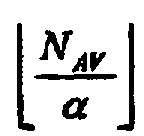
range 1 to α-1 and between I andwhen in the α state. The combination of I and cycle_count counters represent the current status of standby clock generation. At the moment the system switches from the fast clock to slow clock (i.e., high frequency to standby clock), the values of both counters are stored. This corresponds to time T; and the values arc designated I' and cycle_count', and represent state' as shown in Figure 3. Similarly, at the moment the system switches from the slow clock back to the fast clock, the values of both counters (designated I" and cycle_count" and represented as state") are stored. This corresponds to time T2 as shown in Figure 3.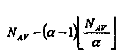
- Using these four values I', I", cycle_count' and cycle_count", the amount of jitter generated can be determined. This jitter error can be compensated for at the time of switching back to active mode by adjusting the fast clock counter (i.e., the bit counter).
- The jitter correction method performed in the jitter calculation processor 42 (Figure 2) will now be described in more detail. A flow diagram illustrating the jitter correction method of the present invention is shown in Figures 7A and 7B. Assuming the communication system is currently in active mode, at some point in time it decides to switch from active mode to standby mode (step 60). This may be determined by an external entity, the communication protocol, the network, etc. To switch modes, the processor configures the select control input to the multiplexer 48 (Figure 2) to select the standby clock. After the selection is performed, the
jitter calculation processor 42 reads the current state' of the state machine (i.e., the current state number I' and number of clocks generated cycle_count' both corresponding to time T1) (step 62). - The
processor 42 then calculates the number of cycles of the available clock source that elapsed from the start of the current state machine cycle up to time T1 (switching from active to standby mode) in accordance withEquation 6 below (step 64).
- The processor then calculates the number of cycles of the available clock source that elapsed from the start of the current state machine cycle up to time T2 in accordance with Equation 7 below (switching from standby to active mode) (step 66).
- The processor then calculates the number of clock cycles generated since the start of dhe current standby mode state machine cycle to time T1 in accordance with Equation 8 below for value of I' = 1 to α-1 and Equation 9 for I' = α (step 68).and
 The particular state (i.e., the value of I') and which equation to use can be determined by evaluating the following. If
 then use Equation 8, otherwise use Equation 9.

- The processor then calculates the number of clock cycles generated since the start of the current standby mode state machine cycle to time T2 in accordance with Equation 11 below for value of I" = 1 to α-1 and
Equation 12 for I" = α (step 70).and The particular state (i.e., the value of I") and which equation to use can be determined by evaluating the following. If
 then use Equation 11, otherwise use

Equation 12. - The jitter J generated is calculated (step 72) for each state at T1 and T2 as follows. For state'Once the jitter error is calculated, the fast clock correction value can be determined and the fast clock counter (i.e., the bit counter) can be modified with the new count value (step 74).
 where FFAST represents the frequency of the fast clock and the current_count_value represents the value the fast counter would normally have been set to without the present invention. Often, the fast counter would be initialized to zero wherein the counter would be initialized with a negative number or the equivalent number modulo the maximum count value (i.e., the number of bits in a frame). Alternatively, the original counter value may be maintained but a portion of the bits of the current frame equal to the jitter error is discarded. Alternatively, the communication system may be caused to 'wake-up' earlier (or later) to account for the time represented by the jitter error in order not to lose any bits in a frame. The decision to switch back to the active state is then made and the new_count_value is loaded into the fast counter(step 76).

- An illustrative example will now be presented. The difference in frequencies of the fast and the available clocks is on the order of approximately 10 to 1. Suppose the desired standby frequency is 3.2 KHz while the available clock is the common frequency 32.768 KHz used to keep time.
- FAV = 32.768 KHz
- FSB = 3.2 KHz The greatest integer common divider GCD is determined to be 128. The values of NAV, NSB and α can be calculated using
- NAV = 256
- NSB = 25
- α = 10
-
- Assume that the state' of the state machine at time T1 of switching from the active mode to the standby mode comprises I' = 4 (current state #4) and cycle_count = 18 cycles counted. The time interval the system is in standby mode is known beforehand: the number of frames NFR = 100 and the number of standby clock cycles in each frame NCL = 50.
- Using these numbers, the values for N'AV and N"AV can be determined using
Equations 6 and 7.Equation 10 evaluates to TRUE, Equation 8 is used to calculate N'SB. Similarly, Equation 13 evaluates to FALSE, thusEquation 12 is used to calculate N"SB.and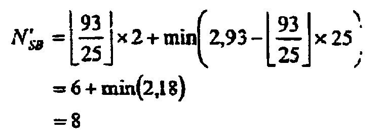 The jitter J is calculated in accordance with
Equation 16 as shown belowAssuming a fast clock rate of 1 MHz, the new count value is given in accordance with
Equation 18 as shown belowThus, the counter is loaded with -225 or as an equivalent is loaded with 775 assuming 1000 bits (or fast clock cycles) per frame. The clock jitter can thus be compensated for by initializing the bit counter to 775.
- It is intended that the appended claims cover all such features and advantages of the invention that fall within the spirit and scope of the present invention. As numerous modifications and changes will readily occur to those skilled in the art, it is intended that the invention not be limited to the limited number of embodiments described herein. Accordingly, it will be appreciated that all suitable variations, modifications and equivalents may be resorted to, falling within the spirit and scope of the present invention.
Claims (25)
- A method of generating a first clock signal having a desired first frequency from an available second clock signal having a second frequency wherein said second frequency is higher than said first frequency, said method comprising the steps of:generating said first clock signal by sequencing through a predetermined number of states whereby during each state a first plurality of cycles of said second clock are absorbed and a second plurality of cycles of said second clock arc output as cycles of said first clock;correcting timing differences between said desired first frequency and said available second frequency at the end of each said sequence by adding a correcting time interval to said first clock such that the average frequency of said first clock is substantially equal to said desired first frequency; andcalculating a compensation interval to compensate for the accumulated timing jitter of said first clock signal during a specified time interval.
- The method according to claim 1. wherein said compensation interval is calculated during a time period ranging from the beginning of the current sequence to a specified point in time.
- The method according to any one of the previous claims, wherein said step of correcting comprises the step of counting a specified number of cycles of said second clock signal so as to compensate for the difference between said first frequency and said second frequency.
- The method according to any one of the previous claims, wherein said step of adding a correcting time interval comprises the step of absorbing a third plurality of cycles of said second clock signal and outputting a fourth plurality of clock cycles of said second clock.
- The method according to any one of the previous claims, wherein said predetermined number of states, termed a, is determined by the ratio of said second frequency to said first frequency.
- The method according to any one of claims 1-4, wherein said predetermined number of stales, termed α, is determined in accordance with the followingwhere

NAV represents the total number of clock cycles of said second clock in one full sequence of states,
NSB represents the total number of clock cycles of said first clock in one full sequence of states,
FAV represents the value of said second frequency, and
FSB represents the value of said first frequency. - The method according to any one of claims 1-4, wherein for all states in said sequence other than the last, said first plurality of cycles is equal towhere NAV = FAV/GCD, wherein a GCD represents the greatest common divisor between said first frequency and said second frequency and a is the ratio of said second frequency to said first frequency.
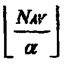
- The method according to any one of claims 1-4, wherein for all states in said sequence other than the last, said second plurality of cycles is equal towhere NSB =FSB/GCD, wherein GCD represents the greatest common divisor between said first frequency and said second frequency and a is the ratio of said second frequency to said first frequency.

- The method according to any one of the previous claims, wherein said step of generating comprises, for the last state in said sequence, absorbing cycles 1 throughof said second clock, where NAV = FAV/GCD, wherein GCD represents the greatest common divisor between said first frequency and said second frequency and a is the ratio of said second frequency to said first frequency.
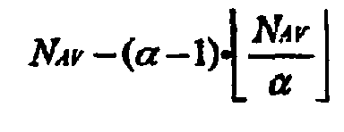
- The method according to any one of claims 1-8, wherein said step of generating comprises, for last state in said sequence, outputtingcycles of said second clock, where NSB = FSB/GCD, wherein GCD represents the greatest common divisor between said first frequency and said second frequency and a is the ratio of said second frequency to said first frequency.

- A method of generating a first clock signal having a desired first frequency from a second clock signal having a second frequency, said method comprising the steps of:counting a first predetermined number of cycles of said second clock signal on a periodic basis;outputting a second predetermined number of cycles of said second clock signal on a periodic basis; andcorrecting accumulated timing differences between said desired first frequency and said second frequency by counting a third predetermined number of cycles of said second clock signal and outputting a fourth predetermined number of cycles of said second clock signal such that the average frequency of said first clock is substantially equal to said desired first frequency.
- The method according to claim 11, further comprising the step of calculating the timing jitter accumulated between a specified interval of time.
- The method according to claim 3 or 12, further comprising the step of providing a third clock signal utilized during an active mode and having a third frequency higher than said first frequency and said second frequency, and adjusting a bit counter associated with said third clock signal in accordance with said calculated timing jitter.
- The method according to any one of claims 11, 12 or 13, wherein said step of correcting comprises the step of counting a specified number of cycles of said second clock signal so as to compensate for the difference between said first frequency and said second frequency.
- The method according to any one of claims 11-14, wherein the periodicity of said steps of counting and outputting is divided into repeating sequences whereby each sequence is divided into a states, the value of a determined in accordance with the followingwhere

NAV represents the total number of clock cycles of said second clock in one full sequence of states,
NSB represents the total number of clock cycles of said first clock in one full sequence of states,
FAV represents the value of said second frequency, and
FSB represents the value of said first frequency. - The method according to claim 15, wherein for all states in said sequence other than the last, said first predetermined number of cycles is equal towhere NAV = TAV/GCD, wherein GCD represents the greatest common divisor between said first frequency and said second frequency.
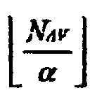
- The method according to claim 15, wherein for all states in said sequence other than the last, said second predetermined number of cycles is equal towhere NSB - FSB/GCD, wherein GCD represents the greatest common divisor between said first frequency and said second frequency.

- In a device having an active and a standby mode of operation, a method of accurately timing the period of time said device is in said standby mode, wherein said device utilizes a standby clock having a desired first frequency generated from an available clock having a second frequency while in standby mode and utilizes a fast clock having a third frequency while in said active mode, said method comprising the steps of:dividing the output of said available clock into continuously repeating sequence of states;for all states but the last in said sequence:counting a first predetermined number of cycles of said available clock signal;outputting as said standby clock a second predetermined number of cycles of said available clock signal;for the last state in said sequence:correcting timing differences accumulated during the current sequence between said desired first frequency and said second frequency by counting a third predetermined number of cycles of said available clock signal and outputting as said standby clock a fourth predetermined number of cycles of said available clock signal such that the average frequency of said standby clock is substantially equal to said desired first frequency;
andcalculating a compensation interval to compensate for the timing error of said standby clock signal accumulated while said device is in standby mode, said compensation interval derived from a jitter value determined in accordance with the total number of cycles of said available clock counted and the total number of cycles of said available clock generated during the current sequence up to the point in time said device switches to active mode. - The method according to claim 18, wherein said first predetermined number is equal tocycles, where NAV - FAV/GCD, wherein GCD represents the greatest common a divisor between said first frequency and said second frequency and a is the rounded ratio of said second frequency to said first frequency.

- The method according to claim 18, wherein said second predetermined number is equal tocycles, where NSB = FSB/GCD, wherein GCD represents the greatest a common divisor between said first frequency and said second frequency and a is the rounded ratio of said second frequency to said first frequency.
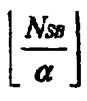
- The method according to claim 15 or 18, wherein said third predetermined number is equal tocycles, where NAV = FAV/GCD, wherein GCD represents the greatest a common divisor between said first frequency and said second frequency and a is the ratio of said second frequency to said first frequency.

- The method according to claim 15 or 18, wherein said fourth predetermined number is equal tocycles, where NSB = FSB/GCD, wherein GCD represents the a greatest common divisor between said first frequency and said second frequency and a is the ratio of said second frequency to said first frequency.
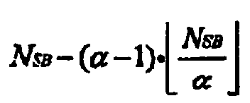
- The method according to any one of the previous claims, wherein said compensation interval comprises the total accumulated jitter as given by
J represents the total accumulated jitter,
FAV represents the value of said second frequency,
FSB represents the value of said first frequency.
N'AVN"AV represent the total number of clock cycles of said available clock accumulated from the beginning of a sequence to the beginning of said specified time interval, and to the end of said specified time interval, respectively, and
N'SB,N"SB represent the total number of clock cycles of said standby clock generated from the beginning of a sequence to the beginning of said specified time interval, and to the end of said specified time interval, respectively. - An apparatus for generating a standby clock frequency in a device having an active and a standby mode of operation, wherein said device utilizes said standby clock having a desired first frequency while in standby mode and utilizes a fast clock having a second frequency while in said active mode, comprising:means for generating said standby clock from an available clock source comprising:means for absorbing a first plurality of cycles of said available clock;means for outputting as said standby clock a second plurality of cycles of said available clock;adjustment means for periodically adjusting for the accumulated timing error caused by the differences in frequencies of said standby clock and said available clock such that the average frequency of said standby clock is substantially equal to said desired first frequency; andmeans for calculating a compensation interval to compensate for the timing error of said standby clock signal accumulated during the time said device was in standby mode, said compensation interval derived from a jitter value determined in accordance with the total number of cycles of said available clock counted and the total number of cycles of said available clock generated during the current sequence up to the point in time said device switches to active mode.
- An apparatus for generating a standby clock frequency in a device having an active and a standby mode of operation, wherein said device utilizes said standby clock having a desired first frequency while in standby mode and utilizes a fast clock having a second frequency while in said active mode, comprising:a clock frequency generator adapted to generate said standby clock from an available clock source, said clock frequency generator comprising:a standby mode state machine operative to:absorb a first plurality of cycles of said available clock;output as said standby clock a second plurality of cycles of said available clock;periodically adjust for the accumulated timing error caused by the differences in frequencies of said standby clock and said available clock such that the average frequency of said standby clock is substantially equal to said desired first frequency; anda jitter calculator adapted to calculate a compensation interval to compensate for the timing error of said standby clock signal accumulated during the time said device was in standby mode, said compensation interval derived from a jitter value determined in accordance with the total number of cycles of said available clock counted and the total number of cycles of said available clock generated during the current sequence up to the point in time said device switches to active mode,
Priority Applications (4)
| Application Number | Priority Date | Filing Date | Title |
|---|---|---|---|
| US09/542,297 US6629256B1 (en) | 2000-04-04 | 2000-04-04 | Apparatus for and method of generating a clock from an available clock of arbitrary frequency |
| CN01116487.5A CN1216470C (en) | 2000-04-04 | 2001-04-04 | Device and method for generating clock with optional frequency usable clock |
| JP2001142429A JP2002026723A (en) | 2000-04-04 | 2001-04-04 | Clock signal generation method and apparatus |
| EP01201261A EP1248373B1 (en) | 2000-04-04 | 2001-04-05 | Apparatus for and method of generating a clock from an available clock of arbitrary frequency |
Applications Claiming Priority (2)
| Application Number | Priority Date | Filing Date | Title |
|---|---|---|---|
| US09/542,297 US6629256B1 (en) | 2000-04-04 | 2000-04-04 | Apparatus for and method of generating a clock from an available clock of arbitrary frequency |
| EP01201261A EP1248373B1 (en) | 2000-04-04 | 2001-04-05 | Apparatus for and method of generating a clock from an available clock of arbitrary frequency |
Publications (2)
| Publication Number | Publication Date |
|---|---|
| EP1248373A1 true EP1248373A1 (en) | 2002-10-09 |
| EP1248373B1 EP1248373B1 (en) | 2011-07-20 |
Family
ID=29737898
Family Applications (1)
| Application Number | Title | Priority Date | Filing Date |
|---|---|---|---|
| EP01201261A Expired - Lifetime EP1248373B1 (en) | 2000-04-04 | 2001-04-05 | Apparatus for and method of generating a clock from an available clock of arbitrary frequency |
Country Status (4)
| Country | Link |
|---|---|
| US (1) | US6629256B1 (en) |
| EP (1) | EP1248373B1 (en) |
| JP (1) | JP2002026723A (en) |
| CN (1) | CN1216470C (en) |
Cited By (3)
| Publication number | Priority date | Publication date | Assignee | Title |
|---|---|---|---|---|
| WO2011064583A1 (en) * | 2009-11-25 | 2011-06-03 | St-Ericsson Sa | Cloc recovery in a battery powered device |
| EP1479167B1 (en) * | 2002-02-27 | 2012-10-10 | Advanced Micro Devices, Inc. | Frequency divider |
| WO2017030755A1 (en) * | 2015-08-19 | 2017-02-23 | Qualcomm Incorporated | Methods and apparatus for synchronizing frequency dividers using a pulse swallowing technique |
Families Citing this family (22)
| Publication number | Priority date | Publication date | Assignee | Title |
|---|---|---|---|---|
| TWI263393B (en) * | 2001-10-15 | 2006-10-01 | Winbond Electronics Corp | Switching method of modulating frequency source and the circuit structure |
| US7188060B1 (en) * | 2002-03-29 | 2007-03-06 | Unisys Corporation | Emulation of a high-speed, high-stability clock |
| JP4082211B2 (en) * | 2002-12-27 | 2008-04-30 | 株式会社デンソー | Microcomputer |
| US8233540B2 (en) * | 2005-03-10 | 2012-07-31 | Qualcomm Incorporated | Method of time base reconstruction for discrete time labeled video |
| US7848318B2 (en) * | 2005-08-03 | 2010-12-07 | Altera Corporation | Serializer circuitry for high-speed serial data transmitters on programmable logic device integrated circuits |
| DE602006013933D1 (en) | 2006-02-10 | 2010-06-10 | Carotech Sdn Bhd Chemor | A process for obtaining highly enriched natural product fractions from palm oil using supercritical and near supercritical fluid media |
| KR100723537B1 (en) * | 2006-09-12 | 2007-05-30 | 삼성전자주식회사 | Clock signal generating method and apparatus and clock frequency control method and apparatus using same |
| US20090080442A1 (en) * | 2007-09-26 | 2009-03-26 | Narayan Ananth S | Conserving power in a multi-node environment |
| JP2009088818A (en) * | 2007-09-28 | 2009-04-23 | Rohm Co Ltd | Information communication terminal, wireless communication device, and wireless communication network |
| US8412105B2 (en) * | 2007-11-26 | 2013-04-02 | Apple Inc. | Electronic devices with radio-frequency collision resolution capabilities |
| DE102008051222B4 (en) | 2008-10-14 | 2017-05-11 | Atmel Corp. | Circuit of a radio system, use and method of operation |
| US8504854B2 (en) | 2010-06-21 | 2013-08-06 | Advanced Micro Devices, Inc. | Managing multiple operating points for stable virtual frequencies |
| US9261949B2 (en) | 2010-10-29 | 2016-02-16 | Advanced Micro Devices, Inc. | Method for adaptive performance optimization of the soc |
| US8682632B1 (en) * | 2011-02-16 | 2014-03-25 | Qlogic, Corporation | Simulation system and method thereof |
| US9229506B1 (en) * | 2012-03-21 | 2016-01-05 | Marvell Israel (M.I.S.L) Ltd. | Dynamic power regulation |
| US9898565B2 (en) * | 2015-11-25 | 2018-02-20 | Synopsys, Inc. | Clock jitter emulation |
| CN106075722B (en) * | 2016-06-03 | 2018-10-16 | 苏州景昱医疗器械有限公司 | The frequency calibrating method and correction system of implantable nerve stimulating apparatus |
| DE202016007417U1 (en) * | 2016-12-03 | 2018-03-06 | WAGO Verwaltungsgesellschaft mit beschränkter Haftung | Control of redundant processing units |
| TWI670593B (en) * | 2018-03-27 | 2019-09-01 | 瑞昱半導體股份有限公司 | Counting circuit of performance monitor unit |
| TWI722590B (en) * | 2019-10-02 | 2021-03-21 | 瑞昱半導體股份有限公司 | Method of adjusting target clock and a wireless device thereof |
| CN111490867B (en) * | 2020-04-26 | 2021-02-12 | 杭州锐讯科技有限公司 | Sampling clock synchronization system and method for distributed application |
| US11994082B1 (en) * | 2023-04-27 | 2024-05-28 | Renesas Electronics Corporation | Semiconductor device |
Citations (5)
| Publication number | Priority date | Publication date | Assignee | Title |
|---|---|---|---|---|
| GB2297884A (en) * | 1995-02-07 | 1996-08-14 | Nokia Mobile Phones Ltd | Power saving arrangement in a mobile telephone |
| US5943613A (en) * | 1996-11-07 | 1999-08-24 | Telefonaktiebolaget Lm Ericsson | Method and apparatus for reducing standby current in communications equipment |
| US5987339A (en) * | 1996-12-27 | 1999-11-16 | Matsushita Electric Industrial Co., Ltd. | Receiving portion of radio communication device |
| WO2000010354A1 (en) * | 1998-08-14 | 2000-02-24 | Qualcomm Incorporated | Synchronisation of a low power clock in a wireless communication device |
| EP1052779A1 (en) * | 1999-05-11 | 2000-11-15 | Koninklijke Philips Electronics N.V. | Processor having adaptable operating frequency |
Family Cites Families (13)
| Publication number | Priority date | Publication date | Assignee | Title |
|---|---|---|---|---|
| US3928813A (en) * | 1974-09-26 | 1975-12-23 | Hewlett Packard Co | Device for synthesizing frequencies which are rational multiples of a fundamental frequency |
| US3976945A (en) * | 1975-09-05 | 1976-08-24 | Hewlett-Packard Company | Frequency synthesizer |
| US4939389A (en) | 1988-09-02 | 1990-07-03 | International Business Machines Corporation | VLSI performance compensation for off-chip drivers and clock generation |
| US5457409A (en) | 1992-08-03 | 1995-10-10 | Advanced Micro Devices, Inc. | Architecture of a multiple array high density programmable logic device with a plurality of programmable switch matrices |
| FR2666184A1 (en) * | 1990-08-24 | 1992-02-28 | Alcatel Radiotelephone | CLOCK WITH DIVISION OF FRACTIONAL FREQUENCY AND SERVING THIS CLOCK. |
| US5517521A (en) * | 1993-06-25 | 1996-05-14 | Digital Wireless Corporation | Method and apparatus for synchronization between real-time sampled audio applications operating full-duplex over a half-duplex radio link |
| SG64286A1 (en) | 1995-10-28 | 1999-04-27 | Inst Of Microelectronics | Multiple clock generation in a baseband simulator for testing a radio frequency section of a mobile communications transceiver |
| US5834956A (en) * | 1995-12-29 | 1998-11-10 | Intel Corporation | Core clock correction in a 2/N mode clocking scheme |
| GB9610801D0 (en) * | 1996-05-23 | 1996-07-31 | Philips Electronics Nv | Frequency generating circuit |
| US5805608A (en) | 1996-10-18 | 1998-09-08 | Samsung Electronics Co., Ltd. | Clock generation for testing of integrated circuits |
| US6157376A (en) * | 1998-09-30 | 2000-12-05 | Genesis Microchip, Corp. | Method and apparatus for generating a target clock signal having a frequency of X/Y times the frequency of a reference clock signal |
| US6157232A (en) * | 1999-03-18 | 2000-12-05 | Nec Corporation | Local clock generator |
| US6289067B1 (en) * | 1999-05-28 | 2001-09-11 | Dot Wireless, Inc. | Device and method for generating clock signals from a single reference frequency signal and for synchronizing data signals with a generated clock |
-
2000
- 2000-04-04 US US09/542,297 patent/US6629256B1/en not_active Expired - Lifetime
-
2001
- 2001-04-04 JP JP2001142429A patent/JP2002026723A/en not_active Abandoned
- 2001-04-04 CN CN01116487.5A patent/CN1216470C/en not_active Expired - Lifetime
- 2001-04-05 EP EP01201261A patent/EP1248373B1/en not_active Expired - Lifetime
Patent Citations (5)
| Publication number | Priority date | Publication date | Assignee | Title |
|---|---|---|---|---|
| GB2297884A (en) * | 1995-02-07 | 1996-08-14 | Nokia Mobile Phones Ltd | Power saving arrangement in a mobile telephone |
| US5943613A (en) * | 1996-11-07 | 1999-08-24 | Telefonaktiebolaget Lm Ericsson | Method and apparatus for reducing standby current in communications equipment |
| US5987339A (en) * | 1996-12-27 | 1999-11-16 | Matsushita Electric Industrial Co., Ltd. | Receiving portion of radio communication device |
| WO2000010354A1 (en) * | 1998-08-14 | 2000-02-24 | Qualcomm Incorporated | Synchronisation of a low power clock in a wireless communication device |
| EP1052779A1 (en) * | 1999-05-11 | 2000-11-15 | Koninklijke Philips Electronics N.V. | Processor having adaptable operating frequency |
Cited By (6)
| Publication number | Priority date | Publication date | Assignee | Title |
|---|---|---|---|---|
| EP1479167B1 (en) * | 2002-02-27 | 2012-10-10 | Advanced Micro Devices, Inc. | Frequency divider |
| WO2011064583A1 (en) * | 2009-11-25 | 2011-06-03 | St-Ericsson Sa | Cloc recovery in a battery powered device |
| EP2333954A1 (en) * | 2009-11-25 | 2011-06-15 | ST-Ericsson SA | Clock recovery in a battery powered device |
| KR20120112413A (en) * | 2009-11-25 | 2012-10-11 | 에스티 에릭슨 에스에이 | Cloc recovery in a battery powered device |
| US8630386B2 (en) | 2009-11-25 | 2014-01-14 | St-Ericsson Sa | Clock recovery in a battery powered device |
| WO2017030755A1 (en) * | 2015-08-19 | 2017-02-23 | Qualcomm Incorporated | Methods and apparatus for synchronizing frequency dividers using a pulse swallowing technique |
Also Published As
| Publication number | Publication date |
|---|---|
| JP2002026723A (en) | 2002-01-25 |
| CN1322075A (en) | 2001-11-14 |
| US6629256B1 (en) | 2003-09-30 |
| CN1216470C (en) | 2005-08-24 |
| EP1248373B1 (en) | 2011-07-20 |
Similar Documents
| Publication | Publication Date | Title |
|---|---|---|
| US6629256B1 (en) | Apparatus for and method of generating a clock from an available clock of arbitrary frequency | |
| US6009319A (en) | Method and apparatus for reducing power consumption in a mobile radio communication device | |
| US7529531B2 (en) | Apparatus and methods for estimating a sleep clock frequency | |
| US5740129A (en) | Real time clock | |
| EP0629324B1 (en) | Apparatus and method for reducing power consumption in a mobile communications receiver | |
| EP0726688B1 (en) | Radio telephone | |
| EP0726687B1 (en) | Radio telephone | |
| US6725067B1 (en) | Method and system for restarting a reference clock of a mobile station after a sleep period with a zero mean time error | |
| US6088602A (en) | High resolution frequency calibrator for sleep mode clock in wireless communications mobile station | |
| JP3555252B2 (en) | Intermittent reception control device | |
| US6397053B1 (en) | Reduction of power consumption with increased standby time in wireless communications device | |
| US20090088194A1 (en) | Single Multi-Mode Clock Source for Wireless Devices | |
| US6311081B1 (en) | Low power operation in a radiotelephone | |
| US20060045215A1 (en) | Method and apparatus for frequency correcting a periodic signal | |
| CN1215266A (en) | High-Resolution Clock Reconstruction for Use in Mobile Communications Devices | |
| US6768725B2 (en) | Receiver, intermittent frame synchronizing method, and portable remote terminal | |
| US6618456B1 (en) | Asynchronous timing oscillator re-synchronizer and method | |
| US6539049B1 (en) | Device and method for maintaining time synchronous with a network master time | |
| US20240393857A1 (en) | Low power low frequency counter for software use | |
| HK1018677B (en) | Methods and apparatus for generating timing signals in a radiocommunication unit |
Legal Events
| Date | Code | Title | Description |
|---|---|---|---|
| PUAI | Public reference made under article 153(3) epc to a published international application that has entered the european phase |
Free format text: ORIGINAL CODE: 0009012 |
|
| AK | Designated contracting states |
Kind code of ref document: A1 Designated state(s): AT BE CH CY DE DK ES FI FR GB GR IE IT LI LU MC NL PT SE TR |
|
| AX | Request for extension of the european patent |
Free format text: AL;LT;LV;MK;RO;SI |
|
| 17P | Request for examination filed |
Effective date: 20030409 |
|
| AKX | Designation fees paid |
Designated state(s): DE FR GB |
|
| GRAP | Despatch of communication of intention to grant a patent |
Free format text: ORIGINAL CODE: EPIDOSNIGR1 |
|
| GRAS | Grant fee paid |
Free format text: ORIGINAL CODE: EPIDOSNIGR3 |
|
| GRAA | (expected) grant |
Free format text: ORIGINAL CODE: 0009210 |
|
| AK | Designated contracting states |
Kind code of ref document: B1 Designated state(s): DE FR GB |
|
| REG | Reference to a national code |
Ref country code: GB Ref legal event code: FG4D |
|
| REG | Reference to a national code |
Ref country code: DE Ref legal event code: R096 Ref document number: 60144982 Country of ref document: DE Effective date: 20110908 |
|
| PLBE | No opposition filed within time limit |
Free format text: ORIGINAL CODE: 0009261 |
|
| STAA | Information on the status of an ep patent application or granted ep patent |
Free format text: STATUS: NO OPPOSITION FILED WITHIN TIME LIMIT |
|
| 26N | No opposition filed |
Effective date: 20120423 |
|
| REG | Reference to a national code |
Ref country code: DE Ref legal event code: R097 Ref document number: 60144982 Country of ref document: DE Effective date: 20120423 |
|
| REG | Reference to a national code |
Ref country code: FR Ref legal event code: PLFP Year of fee payment: 16 |
|
| REG | Reference to a national code |
Ref country code: FR Ref legal event code: PLFP Year of fee payment: 17 |
|
| REG | Reference to a national code |
Ref country code: FR Ref legal event code: PLFP Year of fee payment: 18 |
|
| PGFP | Annual fee paid to national office [announced via postgrant information from national office to epo] |
Ref country code: GB Payment date: 20200327 Year of fee payment: 20 |
|
| PGFP | Annual fee paid to national office [announced via postgrant information from national office to epo] |
Ref country code: FR Payment date: 20200320 Year of fee payment: 20 |
|
| PGFP | Annual fee paid to national office [announced via postgrant information from national office to epo] |
Ref country code: DE Payment date: 20200317 Year of fee payment: 20 |
|
| REG | Reference to a national code |
Ref country code: DE Ref legal event code: R071 Ref document number: 60144982 Country of ref document: DE |
|
| REG | Reference to a national code |
Ref country code: GB Ref legal event code: PE20 Expiry date: 20210404 |
|
| PG25 | Lapsed in a contracting state [announced via postgrant information from national office to epo] |
Ref country code: GB Free format text: LAPSE BECAUSE OF EXPIRATION OF PROTECTION Effective date: 20210404 |