EP1248299A2 - Insulated gate bipolar transistor and method of making the same - Google Patents
Insulated gate bipolar transistor and method of making the same Download PDFInfo
- Publication number
- EP1248299A2 EP1248299A2 EP02007318A EP02007318A EP1248299A2 EP 1248299 A2 EP1248299 A2 EP 1248299A2 EP 02007318 A EP02007318 A EP 02007318A EP 02007318 A EP02007318 A EP 02007318A EP 1248299 A2 EP1248299 A2 EP 1248299A2
- Authority
- EP
- European Patent Office
- Prior art keywords
- base layer
- layer
- type
- impurity
- collector
- Prior art date
- Legal status (The legal status is an assumption and is not a legal conclusion. Google has not performed a legal analysis and makes no representation as to the accuracy of the status listed.)
- Withdrawn
Links
Images

Classifications
-
- H—ELECTRICITY
- H10—SEMICONDUCTOR DEVICES; ELECTRIC SOLID-STATE DEVICES NOT OTHERWISE PROVIDED FOR
- H10D—INORGANIC ELECTRIC SEMICONDUCTOR DEVICES
- H10D12/00—Bipolar devices controlled by the field effect, e.g. insulated-gate bipolar transistors [IGBT]
- H10D12/01—Manufacture or treatment
- H10D12/031—Manufacture or treatment of IGBTs
- H10D12/032—Manufacture or treatment of IGBTs of vertical IGBTs
- H10D12/038—Manufacture or treatment of IGBTs of vertical IGBTs having a recessed gate, e.g. trench-gate IGBTs
-
- H—ELECTRICITY
- H10—SEMICONDUCTOR DEVICES; ELECTRIC SOLID-STATE DEVICES NOT OTHERWISE PROVIDED FOR
- H10P—GENERIC PROCESSES OR APPARATUS FOR THE MANUFACTURE OR TREATMENT OF DEVICES COVERED BY CLASS H10
- H10P10/00—Bonding of wafers, substrates or parts of devices
-
- H—ELECTRICITY
- H10—SEMICONDUCTOR DEVICES; ELECTRIC SOLID-STATE DEVICES NOT OTHERWISE PROVIDED FOR
- H10D—INORGANIC ELECTRIC SEMICONDUCTOR DEVICES
- H10D12/00—Bipolar devices controlled by the field effect, e.g. insulated-gate bipolar transistors [IGBT]
- H10D12/411—Insulated-gate bipolar transistors [IGBT]
- H10D12/441—Vertical IGBTs
- H10D12/461—Vertical IGBTs having non-planar surfaces, e.g. having trenches, recesses or pillars in the surfaces of the emitter, base or collector regions
- H10D12/481—Vertical IGBTs having non-planar surfaces, e.g. having trenches, recesses or pillars in the surfaces of the emitter, base or collector regions having gate structures on slanted surfaces, on vertical surfaces, or in grooves, e.g. trench gate IGBTs
-
- H—ELECTRICITY
- H10—SEMICONDUCTOR DEVICES; ELECTRIC SOLID-STATE DEVICES NOT OTHERWISE PROVIDED FOR
- H10D—INORGANIC ELECTRIC SEMICONDUCTOR DEVICES
- H10D62/00—Semiconductor bodies, or regions thereof, of devices having potential barriers
- H10D62/10—Shapes, relative sizes or dispositions of the regions of the semiconductor bodies; Shapes of the semiconductor bodies
- H10D62/13—Semiconductor regions connected to electrodes carrying current to be rectified, amplified or switched, e.g. source or drain regions
- H10D62/149—Source or drain regions of field-effect devices
- H10D62/151—Source or drain regions of field-effect devices of IGFETs
Definitions
- the present invention relates to a semiconductor power device and, more particularly to, an insulated gate bipolar transistor (IGBT), which is applicable to a power conversion inverter (power converter).
- IGBT insulated gate bipolar transistor
- a power IGBT is now used as a semiconductor power device that has a breakdown voltage of not less than 300V and can flow a higher current therethrough.
- the power IGBT's include two well known structures: a planar type IGBT that has an insulating gate, for example, a flat MOS gate, and a trench type IGBT in which the MOS gate is buried in a trench.
- the trench type IGBT has the trench gate structure in which a number of trench IGBT cells in which the trench-side wall serves as a channel region are arrayed in parallel in a semiconductor substrate.
- the trench type IGBT is said to be more advantageous than the planar type IGBT because it can enjoy a lower channel resistance to thereby, for example, easily reduce the loss.
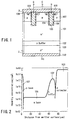
- FIG. 1 is a schematic cross-sectional view for showing part of a conventional trench type IGBT.
- a p type base layer 107 is formed in a surface region of a high-resistance n - type base layer 101.
- a plurality of trenches 104 is formed in a surface region of the p type base layer 107 into the n - type base layer 101.
- a trench gate electrode 106 is buried via a gate insulating film 105.
- a high impurity-concentration n + type emitter layer 108 is formed adjacent the side surface of the trench 104.
- a gate electrode 106 of each trench is drawn out to, for example, a wide gate-electrode contacting pad.
- An emitter electrode 109 is provided on the surfaces of the n + type emitter layer 108 and the p type base layer 107.
- the emitter electrode 109 short-circuits the n + type emitter layer 108 and the p type base layer 107 to each other.
- an inter-layer insulating film 111 is provided on the trench gate electrode 106. The inter-layer insulating film 111 is interposed between the trench gate electrode 106 and the emitter electrode 109 to thereby prevent them from being short-circuited to each other.
- n - type base layer 101, p type base layer 107, n + type emitter layer 108, gate insulating film 105, and trench gate electrode 106 constitute a MOSFET. Electrons are injected from the n + type emitter layer 108 into the n - type base layer 101 through a channel region of the MOSFET. The channel region of the MOSFET is formed at such a surface region of the p type base layer 107 as to be in contact with the trench 104.
- a high impurity-concentration p + type collector layer 103 is formed in the other surface region of the n - type base layer 101 via an n + type buffer layer 102.
- a collector electrode 110 is provided on the p + type collector layer 103.
- n + type buffer layer 102 it is not necessary to form the above-mentioned n + type buffer layer 102 if a desired breakdown voltage can be obtained otherwise.
- E indicates an emitter electrode
- G indicates a gate electrode
- C indicates a collector electrode.
- FIG. 2 shows one example of a distribution of the impurity concentration on a cross section taken along line 2-2 of FIG. 1. As shown in FIG. 2, an n type impurity concentration is constant in the thickness direction of the n - type base layer 101.
- the IGBT having the above-mentioned structure has such a problem that with a decreasing turn-OFF loss, ON-state voltage drop increases extremely in the steady state and, conversely, with the decreasing ON-state voltage drop, the turn-OFF loss increases extremely.
- the thickness of the n - type base layer 101 must be sufficient to obtain a desired breakdown voltage in order to reduce the turn-OFF loss and the ON-state voltage drop in the steady state as much as possible.
- the thickness of the n - type base layer 101 is generally selected according to a relationship of about 10 ⁇ m/100V, for example.
- n + buffer layer is formed by epitaxial growth in a high concentration p + type substrate, in which is in turn formed a relatively high-resistance n - type base layer by epitaxial growth to obtain an n - /n + /p + type three-layer construction wafer in order to form thereon an IGBT having the above-mentioned structure.
- n + type buffer layer 102 and the n - type base layer 101 are thus formed sequentially in the p type substrate by epitaxial growth, meaning that this method increases the manufacture costs of the wafer.
- a wafer manufactured by the floating zone (FZ) method or the Chokralski Zone (CZ) method is ground to a minimum thickness required to obtain a desired breakdown voltage, p type impurities such as boron ions are injected into a surface of the wafer to form a transparent p type collector layer with a thickness of about 1 ⁇ m, thereby form a MOS structure in the other surface of the wafer.
- FZ floating zone
- CZ Chokralski Zone
- the method of using such a thin transparent collector layer has a problem that in order to decrease the ON-state voltage drop and the turn-OFF loss as much as possible, the wafer must be very thin and so very difficult to manufacture.
- the p type base layer 107, the n + type emitter layer 108, the trench 104, the gate insulating film 105, the trench gate electrode 106, and the emitter electrode 109 are formed in a semiconductor substrate, respectively, then the semiconductor substrate is ground to a thickness of 120 ⁇ m, n type and p type impurity ions are implanted to form the n + type buffer layer 102 and the p + type collector layer 103, respectively.
- the above-mentioned methods both have a problem that the wafer may be damaged due to a change in thermal stress during the heat treatment.
- the impurity ions can be activated only down to 1 ⁇ m or so from the wafer surface. It is therefore extremely difficult to form the n + type buffer layer 102 which needs to be deep as much as 1 ⁇ m or more from the wafer surface, by activating and diffusing n type impurity ions. That is, a punch-through type IGBT using the above-mentioned thin semiconductor substrate suffers from a problem in that it is extremely difficult to manufacture.
- n + type emitter layer 108 and the p type base layer 107 are short-circuited to each other via the emitter electrode 109 throughout the surface in a direction parallel to the trench 104.
- the contact opening becomes small in width, thus making it difficult to short-circuit the n + type emitter layer 108 and the p type base layer 107 to each other via the emitter electrode 109 throughout the surface in the direction parallel to the trench 104.
- a suggestion is made to form the n+ type emitter layer 108 of the trench type IGBT so that it may have a ladder-shaped plane pattern, that is, so that the p type base layer 107 may be exposed in a square as much as possible.
- n + type emitter layer 108 may have an overall mesh-shaped or offset mesh-shaped plane pattern, that is, so that a stripe-shaped exposed portion of the n + emitter layer 108 and that of the n type base layer 107 may alternate with each other along the trench 104.
- a trench type IGBT having any one of the above-mentioned various structures also has a problem similar to that of a trench gate type IGBT having the structure shown in FIG. 1. Furthermore, the planar type IGBT has almost the same problem as the trench type IGBT.
- planar type IGBT is known, as disclosed in, for example, Jpn. Pat. Appln. KOKAI No. 11-40808.
- This disclosed planar type IGBT has such an inclination-distributed region in which the impurity concentration is continuously changed that is formed at an n + type buffer layer of n type drift layers, in order to improve the OFF state characteristics without increasing the overall thickness and the turn-ON resistance or the leakage current.
- This planar type IGBT is formed of an n - /n + /p + three-layer structure wafer obtained by forming a high-concentration n + type buffer layer by epitaxial growth on a p + type high-concentration substrate and then forming thereon a relatively high-resistance n - type base layer also by epitaxial growth.
- the turn-OFF loss can be reduced.
- the n + type buffer layer and the n - type base layer are sequentially formed on the p type substrate by epitaxial growth, which raises the problem of increased wafer manufacturing costs.
- the p type collector layer has a considerable thickness, meaning that the overall thickness cannot be reduced.
- the conventional punch-through type IGBT has a problem of a high manufacture cost of an employed semiconductor substrate according to the method of conducting life time control in order to obtain a minimum required turn-OFF loss and the ON-state voltage drop and also has a problem of an extremely thin semiconductor substrate and hence a difficulty in manufacture thereof by the method of using a thin transparent collector layer.
- a semiconductor power device comprises, a first base layer containing an impurity of a first conductivity type so as to have a concentration gradient which continuously changes in a thickness direction thereof, a second base layer containing an impurity of a second conductivity type formed in one surface region of the first base layer, a trench having such a depth as to reach from a surface of the second base layer through the second base layer to the first base layer, an emitter layer containing an impurity of the first conductivity type formed in the surface region of the second base layer in such a manner so as to be in contact with the trench, a gate electrode formed in the trench, a collector layer formed in the other surface of the first base layer, the collector layer contains an impurity of the second conductivity type and has a thickness of 1 ⁇ m or less, a first main electrode continuously formed on the emitter layer and the second base layer, and a second main electrode formed on the collector layer.
- a method for manufacturing a semiconductor power device comprises, introducing an impurity of a first conductivity type into a semiconductor substrate from one surface to form a first base layer, the first base layer having a concentration gradient which continuously changes in a thickness direction thereof, introducing an impurity of a second conductivity type into the first base layer to form a second base layer, introducing an impurity of the first conductivity type into the second base layer to form an emitter layer, forming a trench in the emitter layer, the trench having a depth that reaches through the second base layer to the first base layer, forming a gate electrode in the trench, forming a conductive layer on the resultant structure, then patterning the conductive layer to form a first main electrode continuously on the second base layer and the emitter layer, removing the first base layer from the other surface to provide a desired thickness of the first base layer, introducing an impurity of the second conductivity type into the other surface of the first base layer to form a collector layer, and
- a reference numeral 1 indicates a base layer (n type base layer) having a first conductivity type (n type in this embodiment).
- a base layer (p type base layer) 7 having a second conductivity type (p type in this embodiment) is formed in one surface region of the n type base layer 1.
- a plurality of trenches 4 are formed in the p type base layer 7 having a depth that reaches from the surface of the p type base layer 7 through to the n type base layer 1.
- a high impurity-concentration n type emitter layer (n + type emitter layer) 8 is formed in a surface region of the p type base layer 7 sandwiched by the trenches 4, in contact with the side surface of the trench 4.
- Into each trench 4 is buried a trench gate electrode 6 via a gate insulating film 5.
- an emitter (E) electrode 9 made of, for example, an aluminum is provided on the n + type emitter layer 8 and p type base layer 7.
- An inter-layer insulating film 10 is deposited on the p type base layer 7 and trench gate electrode 6.
- An emitter electrode 9 is formed on the n + type emitter layer 8 and p type base layer 7, to contact with the n+ type emitter layer 8 and the p type base layer 7.
- Each trench gate electrode 6 is drawn out, for example, to a gate contact pad.
- a gate (G) electrode is provided so as to be in contact with the gate contact pad.
- n type base layer 1, p type base layer 7, n + type emitter layer 8, gate insulating film 5, and trench gate electrode 6 make up a MOSFET in which electrons are injected from the n + type emitter layer 8 into the n type base layer 1 through such a portion of a channel region formed in the surface of the p type base layer in contact with the gate insulating film 5 in the trench 4.
- a p type collector layer (p + collector layer) 2 having a high impurity concentration is formed in the other surface region of the n type base layer 1.
- a collector (C) electrode 3 is formed on the p + type collector layer 2.
- a positive voltage is applied to the trench gate electrode 6 with respect to the emitter electrode 9. Accordingly, a surface region in contact with the gate insulating film 5 of the p type base layer 7 is inverted into negative to thereby form an inversion layer, that is an n type channel, through which electrons are injected from the emitter electrode 9 into the n type base layer 1, thus arriving at the p type collector layer 2.
- the junction between the p type collector layer 2 and the n type base layer 1 is forward-biased, thus causing positive holes to be injected from the p type collector layer 2 into the n type base layer 1.
- both the electrons and the holes are injected into the n type base layer 1, as a result of which the n type base layer 1 encounters a conductivity fluctuation in the n type base layer 1 to thereby greatly reduce the resistance of the n type base layer 1, thus turning the device ON.
- a negative voltage is applied to the trench gate electrode 6 with respect to the emitter electrode 9. Accordingly, the above-mentioned n type channel disappears, thus stopping electrons injection.
- the holes accumulated in the n type base layer 1 are partially discharged via the p type base layer 7 to the emitter electrode 9, while at the same time the other holes are recombined with electrons to be neutralized, thus turning it OFF.
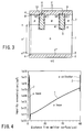
- FIG. 4 shows one example of the impurity concentration distribution on a cross section taken along line 4-4 of FIG. 3.
- the thickness of the n type base layer 1 can be selected at a step of about 10 ⁇ m/100 by providing the n type base layer 1 with such an impurity concentration gradient that its collector-layer side portion may have a higher concentration than its emitter-layer side portion, setting the specific resistance of the emitter-layer side of the n type base layer 1 at 100 ⁇ cm or higher, and setting the concentration peak (maximum concentration) of the collector-layer side of the n type base layer 1 at not less than 1e15/cm 3 but not higher than 5e16/cm 3 .
- the conventional punch-through type IGBT has employed either a method of stopping at the n + type buffer layer 102 the spread of a depletion layer extending from the p type base layer 107 shown in FIG. 1 or a method of providing a sufficient thickness of the n - type base layer 101 to thereby prevent the depletion layer from reaching the p + type collector layer 103.
- the IGBT according to this embodiment utilizes such a principle that the width of the depletion layer derived from Poisson's Equation is inversely proportional to an impurity concentration gradient, to effectively inhibit the spread of the deletion layer by the impurity concentration gradient of the n type base layer 1, thus preventing the depletion layer from reaching the p + type collector layer 2.
- the IGBT according to the above embodiment is capable of greatly reducing the thickness of the p type collector layer 2 as compared to that of the p type collector layer 103 of the conventional punch-through type IGBT, thus greatly decreasing the overall thickness as compared to the conventional punch-through type IGBT.
- Table 1 indicates a survey result of simulating a relationship between the specific resistance and the breakdown voltage of the emitter-side portion of the n type base layer 1 with the concentration peak of its collector side portion fixed at a certain value.
- Specific resistance ( ⁇ cm) 40 k 900 400 100 Breakdown voltage (V) 720 671 645 607
- Table 1 shows that the IGBT according to the above embodiment exhibits a breakdown voltage of 600V or higher by setting the specific resistance of the emitter-side portion of the n type base layer 1 at 100 ⁇ cm or higher and that the thickness of the n type base layer 1 can be selected at a step of 10 ⁇ m/100V.
- the thickness of the n type base layer 1 of the IGBT according to the above embodiment can be selected at a step of about 10 ⁇ m/100V, as in the conventional punch-through type IGBT.
- a conventional punch-through type IGBT containing an n - type base layer having a constant specific resistance can enjoy a breakdown voltage of 600V or higher with a thickness of 60 ⁇ m, and the thickness can be selected at steps of about 10 ⁇ m/100V.
- Table 2 indicates a survey result of simulating the relationship between the concentration peak and the breakdown voltage of the collector-side portion of the n type base layer 1 with the specific resistance of its emitter-side portion fixed to 40 k ⁇ cm in a case where its thickness is set at 60 ⁇ m.
- Table 2 shows that in the IGBT according to the above embodiment, the breakdown voltage of the collector-side portion of the n type base layer 1 gradually increases to its maximum value as its concentration peak is increased from 8e14/cm 3 to 2e15/cm 3 .
- the breakdown voltage decreases from the maximum gradually and, when it further exceeds the value of 5e16/cm 3 , falls down to 600V or lower.
- the breakdown voltage becomes 600V or higher and that the thickness of the n type base layer 1 can be selected at steps of about 10 ⁇ m/100V.
- the relationship between the impurity concentration gradient and the breakdown voltage of the collector-side portion of the n type base layer 1 indicates that the impurity concentration gradient must be 1e18/cm 3 to 5e19/cm 3 in order to give the breakdown voltage of 600V or higher.
- the IGBT according to the above embodiment may in some cases have a region where the specific resistance of the emitter-layer side portion of the n type base layer 1 stays constant therethrough. This phenomenon occurs because when n type impurities are diffused into one surface region of the n type semiconductor substrate to form the n type base layer 1, the thickness of the formed diffusion layer of the n type impurity fluctuates due to fluctuations in the diffusion conditions such as the thickness and specific resistance of the n type semiconductor substrate and the surface concentration and diffusion time of the n type impurity.
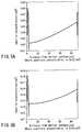
- FIGS. 5A and 5B show one example of the depth-directional impurity concentration distribution in a case where the thickness of a semiconductor substrate to form thereon the n type base layer 1 of the IGBT according to the above embodiment is 90 ⁇ m and the emitter-layer side portion has a different specific resistance, each other.
- these two impurity concentration distributions indicate that such a region of the emitter-layer side portion of the n type base layer 1 that has a constant specific resistance changes according to the specific resistance of the semiconductor substrate.
- this constant specific resistance is suppressed to 30 ⁇ m or so, taking the electric characteristics into account.
- the specific resistance may stay constant within a depth of 30 ⁇ m from the surface in the emitter-layer side portion of the n type base layer 1, depending on the fluctuations in the amount of the impurity diffused into the semiconductor substrate.
- the IGBT utilizes the principle that the width of the depletion layer derived from the Poisson's Equation is inversely proportional to an impurity concentration gradient, to effectively inhibit the spread of the deletion layer by the impurity concentration gradient of the n type base layer 1, thus preventing the depletion layer from reaching the p + type collector layer 102.
- the conventional IGBT has employed either the method of stopping, at the n+ type buffer layer 102, the spread of the depletion layer extending from the p type base layer 107 or the method of providing a sufficient thickness of the n - type base layer 101 to thereby prevent the depletion layer from reaching the p+ type collector layer 103.
- the region where the specific resistance of the emitter-side portion of the n type base layer 1 stays constant is extremely smaller in length than the n - type base layer 101 where the specific resistance stays constant in the conventional punch-through type IGBT.
- the following compares the IGBT according to the above embodiment and the conventional punch-through type IGBT which have a breakdown voltage of 600V to each other in terms of ON-state voltage drop and fall time.
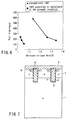
- FIG. 6 is a graph for showing a simulation result of the ON-state voltage drop and the fall time of the IGBT according to the above embodiment and the conventional punch-through type IGBT, in which the horizontal axis indicates a voltage and the vertical axis indicates a time.
- n type base layer 1 of the IGBT with a gradient in impurity concentration distribution, it is possible to minimize the turn-OFF loss and the ON-state voltage drop while at the same time sustaining a desired breakdown voltage, to thereby greatly reduce the thickness of a semiconductor substrate employed, that is to reduce it to a minimum.
- the following describes a method of manufacturing an IGBT having the structure shown in FIG. 3.
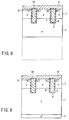
- FIGS. 7 to 9 are cross-sectional views for showing main steps of manufacturing the IGBT according to the embodiment shown in FIG. 3.
- an n type semiconductor substrate is prepared for forming the n type base layer 1 thereon.
- an n type impurity is thermally diffused into the semiconductor substrate having a specific resistance of 100 ⁇ cm to thereby provide the substrate with such an impurity concentration gradient that its one side surface may have a lower impurity concentration than the other side surface.
- the n type semiconductor substrate having such an impurity concentration distribution is used as a material of the n type base layer 1 to form the p type base layer 7 by diffusion in the one surface region of the n type substrate.
- the n + type emitter layer 8 is formed by diffusion in the surface region of the p type base layer 7 in such a manner that it may have a number of stripe-shaped plane patterns.
- an exposed portion of the p type base layer 7 also has a number of the stripe-shaped plane patterns.
- the trench 4 which has the striped-shaped plane patter and also a depth that reaches to the n type base layer 1, is formed in each n+ type emitter layer 8. That is, this depth of thus formed trench 4 reaches from the surface of the n + type emitter layer 8 through the n+ type emitter layer 8 and the p type base layer 7 to the n type base layer 1.
- the gate insulating film 5 made of SiO 2 etc. is formed on the inner surface of the trench 4 and the substrate.
- the poly-silicon 6 containing phosphorus (P) is deposited by chemical vapor deposition (CVD) and then buried into the trench 4 to serve as a trench gate electrode.
- the substrate is patterned according to a trench-gate draw-out pattern for drawing out the trench gate electrode 6 to thereby form a gate electrode-contacting wide pad and also etch back the upper surface of the poly-silicon 6 in the trench so that it may be flat with the substrate surface.
- the inter-layer insulating film 10 is deposited on the substrate to then form a wide contact hole for drawing out the gate electrode in the inter-layer insulating film 10 on the pad and also form a contact hole for drawing out the emitter/base both in the inter-layer insulating film 10 in the periphery of the trench opening and in the underlying gate insulating film 5 on the substrate surface.
- an aluminum layer is formed by sputtering on the substrate to then perform predetermined patterning thereon, thus forming the emitter electrode 9 and the gate electrode.
- the n type base layer 1 on the other hand, needs to be as thick as about 60 ⁇ m in order to have a breakdown voltage of, for example, 600V, so that as shown in FIG. 8, it is ground from the other surface of the n type substrate, that is, the back side surface of the substrate, to be reduced to 60 ⁇ m in thickness.
- the depth-directional impurity concentration distribution of the n type base layer 1 is such as shown in FIG. 4.
- ions of a p type impurity such as boron are implanted into the ground surface of the n type base layer 1, which is then annealed by means of, for example, pulse laser application to thereby activate the p type impurity, thus forming the p type collector layer 2. Then, the collector electrode 3 is formed.
- a p type impurity such as boron
- the p type collector layer 2 is as thick as 1 ⁇ m or less and the surface concentration of the impurity on the side of the collector electrode 3 is 1e17/cm 3 or more.
- a trench IGBT is manufactured which has the n type base layer 1 with a thickness of 60 ⁇ m and the p type collector layer 2 with a small thickness of 1 ⁇ m or less.
- a conventionally suggested method may be used to sufficiently short-circuit the n + type emitter layer 8 and the p type base layer 7 to each other using the emitter electrode 9 even when the cell pitch is reduced in the trench type IGBT having the structure shown in FIG. 3.
- the IGBT may be formed so that the n + type emitter layer 8 would have a ladder-shaped plane pattern, that is, so that the p type base layer 7 would be exposed in a square as many as possible. Further, the IGBT may be formed so that the n + type emitter layer 8 would have an overall mesh-shaped or offset mesh-shaped plane pattern, that is, so that a stripe-shaped exposed portion of the n + emitter layer 8 and that of the n type base layer 7 would alternate with each other along the trench 4.
- a trench contact structure may be employed whereby an emitter contact trench is formed in the p type base layer 7 between the mutually opposing n + type emitter layers 8 so that the emitter electrode 9 may be formed in the trench in such a manner as to come in contact with the side surface of the n + type emitter layer 8 and the p type base layer 7.
- the present invention is applied to a planar type IGBT having a planar gate structure.
- the planar type IGBT has such a planar gate structure that a gate electrode is formed on a gate insulating film formed on a p type base layer with a gate structure different from that of the trench type IGBT shown in FIG. 3, the device structure of which is shown in the cross-sectional view of FIG. 10. It is here to be noted that the same components of FIG. 10 as those of FIG. 3 are indicated by the same reference symbols and their description is omitted.
- the n type base layer 1 is provided with an impurity concentration gradient so that its collector-layer side portion may have a higher impurity concentration than its emitter-layer side portion; specifically, the specific resistance of the emitter-layer side portion is set at 100 ⁇ cm or higher and the concentration peak of the collector-layer side portion is set at 1e15/cm 3 or higher and 5e16/cm 3 or lower. Further, the p type collector layer 2 has a thickness of 1 ⁇ m or less and the collector electrode 3 has a surface impurity concentration of 1e17/cm 3 .
- planar type IGBT has also the same effects as those of the trench type IGBT shown in FIG. 3.
- a wiring line electrically connected to the collector layer may be drawn out to a place other than the collector layer to then provide the collector electrode thereon.
Landscapes
- Electrodes Of Semiconductors (AREA)
- Thyristors (AREA)
- Bipolar Transistors (AREA)
Abstract
Description
| Specific resistance (Ω·cm) | 40 k | 900 | 400 | 100 |
| Breakdown voltage (V) | 720 | 671 | 645 | 607 |
| Concentration peak (/cm3) | 8e14 | 1e15 | 2e15 | 6e15 | 2e16 | 5e16 |
| Breakdown voltage (V) | 365 | 602 | 720 | 673 | 659 | 610 |
Claims (18)
- A semiconductor power device characterized by comprising:a first base layer (1) containing an impurity of a first conductivity type so as to have a concentration gradient which continuously changes in a thickness direction thereof;a second base layer (7) containing an impurity of a second conductivity type formed in one surface region of said first base layer;a trench (4) having such a depth as to reach from a surface of said second base layer through said second base layer to said first base layer;an emitter layer (8) containing an impurity of said first conductivity type formed in the surface region of said second base layer in such a manner so as to be in contact with said trench;a gate electrode (6) formed in said trench;a collector layer (2) formed in the other surface of said first base layer, said collector layer contains an impurity of said second conductivity type and has a thickness of 1 µm or less;a first main electrode (9) continuously formed on said emitter layer and said second base layer; anda second main electrode (3) formed on said collector layer.
- The semiconductor power device according to claim 1, characterized in that a concentration of said impurity at one end of said first base layer (1) positioned on the side of said collector layer (2) is in a range of 1e15/cm3 to 5e16/cm3, and a concentration of said impurity at the other end of said first base layer (1) positioned on the side of said second base layer (7) is 1e11/cm3.
- The semiconductor power device according to claim 1, characterized in that a specific resistance at said one end of said first base layer (1) positioned on the side of said collector layer (2) is 100 Ω·cm or higher.
- The semiconductor power device according to claim 1, characterized in that a surface impurity concentration of said collector layer (2) on the side of said second main electrode (3) is 1e17/cm3 or higher.
- The semiconductor power device according to claim 1, characterized in that the specific resistance at a depth of 30 µm or less as measured from said one end of said first base layer (1) on the side of said second base layer (2) is constant at 100 Ω·cm or higher.
- The semiconductor power device according to claim 1, characterized in that said first conductivity type is an n type and said second conductivity type is a p type.
- A semiconductor power device comprising:a first base layer (1) containing an impurity of a first conductivity type so as to have a concentration gradient which continuously changes in a thickness direction thereof;a second base layer (7) containing an impurity of a second conductivity type formed in one surface region of said first base layer;an emitter layer (8) containing an impurity of said first conductivity type formed in a surface region of said second base layer;a gate electrode (6) continuously formed at least on said second base layer (7) and said emitter layer (8);a collector layer (2) formed on the other surface of said first base layer, said collector layer contains an impurity of said second conductivity type and has a thickness of 1 µm or less;a first main electrode (9) formed on said second base layer; anda second main electrode formed on said collector layer.
- The semiconductor power device according to claim 7, characterized in that a concentration of said impurity at one end of said first base layer (1) positioned on the side of said collector layer (2) is in a range of 1e15/cm3 to 5e16/cm3 and a concentration of said impurity at the other end of said first base layer (1) positioned on the side of said second base layer (7) is 1e11/cm3.
- The semiconductor power device according to claim 7, characterized in that a specific resistance at said one end of said first base layer (1) positioned on the side of said collector layer (2) is 100 Ω·cm or higher.
- The semiconductor power device according to claim 7, characterized in that a surface impurity concentration of said one end of said collector layer on the side of said second main electrode (3) is 1e17/cm3 or higher.
- The semiconductor power device according to claim 7, characterized in that the specific resistance at a depth of 30 µm or less as measured from said one end of said first base layer (1) on the side of said second base layer (2) is constant at 100 Ω·cm or higher.
- The semiconductor power device according to claim 7, characterized in that said first conductivity type is an n type and said second conductivity type is a p type.
- A method for manufacturing a semiconductor power device comprising:introducing an impurity of a first conductivity type into a semiconductor substrate from one surface to form a first base layer (1), said first base layer having a concentration gradient which continuously changes in a thickness direction thereof;introducing an impurity of a second conductivity type into said first base layer to form a second base layer (7);introducing an impurity of said first conductivity type into said second base layer to form an emitter layer (8);forming a trench (4) in said emitter layer, said trench having a depth that reaches through said second base layer to said first base layer;forming a gate electrode (6) in said trench;forming a conductive layer on the resultant structure, then patterning said conductive layer to form a first main electrode (9) continuously on said second base layer and said emitter layer (8);removing said first base layer (1) from the other surface to provide a desired thickness of said first base layer (1);introducing an impurity of said second conductivity type into said other surface of said first base layer (1) to form a collector layer (2); andforming a second main electrode on an exposed surface of said collector layer (2).
- The method according to claim 13, characterized in that said first base layer (1) is formed so that a concentration of said impurity at one end of said first base layer (1) positioned on the side of said collector layer (2) is set in a range of 1e15/cm3 to 5e16/cm3 and a concentration of said impurity at the other end of said first base layer (1) positioned on the side of said second base layer (7) is set 1e11/cm3.
- The method according to claim 13, characterized in that said first base layer (1) is formed so that a specific resistance at said one end of said first base layer (1) positioned on the side of said collector layer (2) is 100 Ω·cm or higher.
- The method according to claim 13, characterized in that said collector layer (2) is formed so that a surface impurity concentration of said collector layer (2) on the side of said second main electrode (3) is 1e17/cm3 or higher.
- The method according to claim 13, characterized in that said first base layer (1) is formed so that the specific resistance at a depth of 30 µm or less as measured from said one end of said first base layer (1) on the side of said second base layer (2) is constant at 100 Ω·cm or higher.
- The method according to claim 13, characterized in that said first conductivity type is an n type and said second conductivity type is a p type.
Applications Claiming Priority (2)
| Application Number | Priority Date | Filing Date | Title |
|---|---|---|---|
| JP2001107252 | 2001-04-05 | ||
| JP2001107252A JP2002305304A (en) | 2001-04-05 | 2001-04-05 | Power semiconductor device |
Publications (2)
| Publication Number | Publication Date |
|---|---|
| EP1248299A2 true EP1248299A2 (en) | 2002-10-09 |
| EP1248299A3 EP1248299A3 (en) | 2008-05-28 |
Family
ID=18959602
Family Applications (1)
| Application Number | Title | Priority Date | Filing Date |
|---|---|---|---|
| EP02007318A Withdrawn EP1248299A3 (en) | 2001-04-05 | 2002-04-04 | Insulated gate bipolar transistor and method of making the same |
Country Status (6)
| Country | Link |
|---|---|
| US (2) | US6605858B2 (en) |
| EP (1) | EP1248299A3 (en) |
| JP (1) | JP2002305304A (en) |
| KR (1) | KR100449182B1 (en) |
| CN (1) | CN1228858C (en) |
| TW (1) | TW567615B (en) |
Cited By (1)
| Publication number | Priority date | Publication date | Assignee | Title |
|---|---|---|---|---|
| EP1453105A3 (en) * | 2003-02-26 | 2006-04-19 | Toyota Jidosha Kabushiki Kaisha | Vertical field effect transistor having a high withstand voltage |
Families Citing this family (45)
| Publication number | Priority date | Publication date | Assignee | Title |
|---|---|---|---|---|
| JP2002305304A (en) * | 2001-04-05 | 2002-10-18 | Toshiba Corp | Power semiconductor device |
| JP3732814B2 (en) * | 2002-08-15 | 2006-01-11 | 株式会社東芝 | Semiconductor device |
| CN101330103B (en) * | 2003-08-27 | 2010-06-02 | 三菱电机株式会社 | Insulated gate transistor and inverter circuit |
| JP4768231B2 (en) * | 2004-03-18 | 2011-09-07 | ルネサスエレクトロニクス株式会社 | Manufacturing method of semiconductor device |
| US7423316B2 (en) * | 2004-05-12 | 2008-09-09 | Kabushiki Kaisha Toyota Chuo Kenkyusho | Semiconductor devices |
| JP2005354031A (en) * | 2004-05-13 | 2005-12-22 | Mitsubishi Electric Corp | Semiconductor device |
| JP4575713B2 (en) * | 2004-05-31 | 2010-11-04 | 三菱電機株式会社 | Insulated gate semiconductor device |
| DE102005040624A1 (en) * | 2004-09-02 | 2006-03-09 | Fuji Electric Holdings Co., Ltd., Kawasaki | Semiconductor component and method for its production |
| US20060049464A1 (en) | 2004-09-03 | 2006-03-09 | Rao G R Mohan | Semiconductor devices with graded dopant regions |
| JP4791723B2 (en) * | 2004-10-18 | 2011-10-12 | 株式会社東芝 | Semiconductor device and manufacturing method thereof |
| US7723803B2 (en) * | 2005-03-07 | 2010-05-25 | Taiwan Semiconductor Manufacturing Co., Ltd. | Bipolar device compatible with CMOS process technology |
| JP5033335B2 (en) * | 2006-02-21 | 2012-09-26 | ルネサスエレクトロニクス株式会社 | Semiconductor device and inverter device using the same |
| JP5112648B2 (en) * | 2006-05-29 | 2013-01-09 | セイコーインスツル株式会社 | Semiconductor device |
| JP5128100B2 (en) * | 2006-09-29 | 2013-01-23 | 三菱電機株式会社 | Power semiconductor device |
| US8093621B2 (en) | 2008-12-23 | 2012-01-10 | Power Integrations, Inc. | VTS insulated gate bipolar transistor |
| DE102007020657B4 (en) * | 2007-04-30 | 2012-10-04 | Infineon Technologies Austria Ag | Semiconductor device with a semiconductor body and method for producing the same |
| JP5261982B2 (en) * | 2007-05-18 | 2013-08-14 | 富士電機株式会社 | Semiconductor device and manufacturing method of semiconductor device |
| JP2008305998A (en) * | 2007-06-07 | 2008-12-18 | Fuji Electric Device Technology Co Ltd | Semiconductor device |
| JP5564763B2 (en) * | 2008-06-05 | 2014-08-06 | 富士電機株式会社 | Method for manufacturing MOS type semiconductor device |
| US7964912B2 (en) | 2008-09-18 | 2011-06-21 | Power Integrations, Inc. | High-voltage vertical transistor with a varied width silicon pillar |
| US20100155831A1 (en) * | 2008-12-20 | 2010-06-24 | Power Integrations, Inc. | Deep trench insulated gate bipolar transistor |
| US7871882B2 (en) | 2008-12-20 | 2011-01-18 | Power Integrations, Inc. | Method of fabricating a deep trench insulated gate bipolar transistor |
| JP2010232335A (en) * | 2009-03-26 | 2010-10-14 | Sanyo Electric Co Ltd | Insulated gate bipolar transistor |
| US8330214B2 (en) * | 2009-05-28 | 2012-12-11 | Maxpower Semiconductor, Inc. | Power semiconductor device |
| JP2010283132A (en) * | 2009-06-04 | 2010-12-16 | Mitsubishi Electric Corp | Semiconductor device |
| EP2317553B1 (en) * | 2009-10-28 | 2012-12-26 | STMicroelectronics Srl | Double-sided semiconductor structure and method for manufacturing the same |
| KR101811895B1 (en) * | 2010-03-23 | 2017-12-22 | 에이비비 슈바이쯔 아게 | Power semiconductor device |
| JP6006918B2 (en) | 2011-06-06 | 2016-10-12 | ルネサスエレクトロニクス株式会社 | SEMICONDUCTOR DEVICE, SEMICONDUCTOR DEVICE MANUFACTURING METHOD, AND ELECTRONIC DEVICE |
| CN103151251B (en) * | 2011-12-07 | 2016-06-01 | 无锡华润华晶微电子有限公司 | Trench-type insulated gate bipolar transistor and preparation method thereof |
| JP5644793B2 (en) * | 2012-03-02 | 2014-12-24 | 株式会社デンソー | Semiconductor device |
| CN103367436B (en) * | 2012-04-03 | 2017-08-08 | 朱江 | A kind of groove Schottky MOS semiconductor device and its manufacture method |
| US8653600B2 (en) | 2012-06-01 | 2014-02-18 | Power Integrations, Inc. | High-voltage monolithic schottky device structure |
| JP5880311B2 (en) * | 2012-06-26 | 2016-03-09 | 住友電気工業株式会社 | Silicon carbide semiconductor device |
| CN103151371A (en) * | 2013-03-05 | 2013-06-12 | 矽力杰半导体技术(杭州)有限公司 | Wafer structure and power device by using same |
| JP2015023118A (en) * | 2013-07-18 | 2015-02-02 | 株式会社東芝 | Semiconductor device |
| US10325988B2 (en) | 2013-12-13 | 2019-06-18 | Power Integrations, Inc. | Vertical transistor device structure with cylindrically-shaped field plates |
| US9543396B2 (en) | 2013-12-13 | 2017-01-10 | Power Integrations, Inc. | Vertical transistor device structure with cylindrically-shaped regions |
| CN103855206A (en) * | 2014-02-18 | 2014-06-11 | 宁波达新半导体有限公司 | Insulated gate bipolar transistor and manufacturing method thereof |
| JP6287407B2 (en) * | 2014-03-19 | 2018-03-07 | サンケン電気株式会社 | Semiconductor device |
| JP6126150B2 (en) * | 2015-03-06 | 2017-05-10 | トヨタ自動車株式会社 | Semiconductor device |
| US10002870B2 (en) * | 2016-08-16 | 2018-06-19 | Texas Instruments Incorporated | Process enhancement using double sided epitaxial on substrate |
| JP6880669B2 (en) * | 2016-11-16 | 2021-06-02 | 富士電機株式会社 | Silicon Carbide Semiconductor Device and Method for Manufacturing Silicon Carbide Semiconductor Device |
| CN107464842A (en) * | 2017-08-03 | 2017-12-12 | 电子科技大学 | A kind of superjunction with colelctor electrode groove is against conductivity type IGBT |
| CN115148601A (en) * | 2021-03-30 | 2022-10-04 | 无锡华润华晶微电子有限公司 | Semiconductor structure and method of making the same |
| JP7607538B2 (en) * | 2021-09-14 | 2024-12-27 | 三菱電機株式会社 | Semiconductor Device |
Family Cites Families (23)
| Publication number | Priority date | Publication date | Assignee | Title |
|---|---|---|---|---|
| JPS5942989B2 (en) * | 1977-01-24 | 1984-10-18 | 株式会社日立製作所 | High voltage semiconductor device and its manufacturing method |
| US5173435A (en) * | 1987-11-11 | 1992-12-22 | Mitsubishi Denki Kabushiki Kaisha | Insulated gate bipolar transistor |
| JPH01140808A (en) * | 1987-11-26 | 1989-06-02 | Nec Corp | Transfer gate switching circuit |
| US5004705A (en) * | 1989-01-06 | 1991-04-02 | Unitrode Corporation | Inverted epitaxial process |
| US5466951A (en) * | 1993-12-08 | 1995-11-14 | Siemens Aktiengesellschaft | Controllable power semiconductor element with buffer zone and method for the manufacture thereof |
| US5643821A (en) * | 1994-11-09 | 1997-07-01 | Harris Corporation | Method for making ohmic contact to lightly doped islands from a silicide buried layer and applications |
| US6001678A (en) * | 1995-03-14 | 1999-12-14 | Mitsubishi Denki Kabushiki Kaisha | Insulated gate semiconductor device |
| US5714775A (en) * | 1995-04-20 | 1998-02-03 | Kabushiki Kaisha Toshiba | Power semiconductor device |
| US6693310B1 (en) * | 1995-07-19 | 2004-02-17 | Mitsubishi Denki Kabushiki Kaisha | Semiconductor device and manufacturing method thereof |
| JP3352592B2 (en) * | 1996-05-16 | 2002-12-03 | 三菱電機株式会社 | Semiconductor device and method of manufacturing the same |
| KR100228719B1 (en) * | 1996-05-27 | 1999-11-01 | 윤덕용 | Manufacturing method for soi type semiconductor material that use electrochemical etching method and active drive liquid crystal display device |
| US5807783A (en) * | 1996-10-07 | 1998-09-15 | Harris Corporation | Surface mount die by handle replacement |
| JPH1140808A (en) | 1997-05-21 | 1999-02-12 | Toyota Motor Corp | Semiconductor device and manufacturing method thereof |
| EP1097481B1 (en) * | 1998-07-17 | 2004-03-31 | Infineon Technologies AG | Power semiconductor component for high blocking voltages |
| JP3924975B2 (en) * | 1999-02-05 | 2007-06-06 | 富士電機デバイステクノロジー株式会社 | Trench type insulated gate bipolar transistor |
| JP2001024184A (en) * | 1999-07-05 | 2001-01-26 | Fuji Electric Co Ltd | Insulated gate transistor and manufacturing method thereof |
| US6140170A (en) * | 1999-08-27 | 2000-10-31 | Lucent Technologies Inc. | Manufacture of complementary MOS and bipolar integrated circuits |
| JP2001237249A (en) * | 2000-02-21 | 2001-08-31 | Hitachi Ltd | Semiconductor device and method of manufacturing the same |
| JP4371521B2 (en) * | 2000-03-06 | 2009-11-25 | 株式会社東芝 | Power semiconductor device and manufacturing method thereof |
| JP2001338930A (en) * | 2000-05-29 | 2001-12-07 | Nec Corp | Semiconductor device and semiconductor manufacturing method |
| JP3764343B2 (en) * | 2001-02-28 | 2006-04-05 | 株式会社東芝 | Manufacturing method of semiconductor device |
| US20020137264A1 (en) * | 2001-03-23 | 2002-09-26 | Ming-Jer Kao | Method of fabrication thin wafer IGBT |
| JP2002305304A (en) * | 2001-04-05 | 2002-10-18 | Toshiba Corp | Power semiconductor device |
-
2001
- 2001-04-05 JP JP2001107252A patent/JP2002305304A/en active Pending
-
2002
- 2002-04-02 TW TW091106614A patent/TW567615B/en not_active IP Right Cessation
- 2002-04-04 EP EP02007318A patent/EP1248299A3/en not_active Withdrawn
- 2002-04-04 US US10/115,030 patent/US6605858B2/en not_active Expired - Lifetime
- 2002-04-04 KR KR10-2002-0018534A patent/KR100449182B1/en not_active Expired - Fee Related
- 2002-04-05 CN CNB021061475A patent/CN1228858C/en not_active Expired - Fee Related
-
2003
- 2003-06-10 US US10/457,544 patent/US7056779B2/en not_active Expired - Lifetime
Cited By (1)
| Publication number | Priority date | Publication date | Assignee | Title |
|---|---|---|---|---|
| EP1453105A3 (en) * | 2003-02-26 | 2006-04-19 | Toyota Jidosha Kabushiki Kaisha | Vertical field effect transistor having a high withstand voltage |
Also Published As
| Publication number | Publication date |
|---|---|
| US7056779B2 (en) | 2006-06-06 |
| KR20020077659A (en) | 2002-10-12 |
| JP2002305304A (en) | 2002-10-18 |
| CN1379479A (en) | 2002-11-13 |
| EP1248299A3 (en) | 2008-05-28 |
| US6605858B2 (en) | 2003-08-12 |
| US20020195656A1 (en) | 2002-12-26 |
| TW567615B (en) | 2003-12-21 |
| KR100449182B1 (en) | 2004-09-18 |
| CN1228858C (en) | 2005-11-23 |
| US20030209781A1 (en) | 2003-11-13 |
Similar Documents
| Publication | Publication Date | Title |
|---|---|---|
| US7056779B2 (en) | Semiconductor power device | |
| JP6501331B2 (en) | Trench gate type MOS semiconductor device | |
| US10797167B2 (en) | Superjunction semiconductor device and method of manufacturing the same | |
| US7211837B2 (en) | Insulated gate semiconductor device | |
| CN103875074B (en) | Insulated gate transistor and method of production thereof | |
| EP3659180B1 (en) | Insulated gate power semiconductor device and method for manufacturing such device | |
| KR100223198B1 (en) | Semiconductor device having high breakdown voltage and method of manufacturing the same | |
| CN103650148B (en) | Igbt | |
| US9653595B2 (en) | Semiconductor device and semiconductor device fabrication method | |
| EP1132970A2 (en) | Power semiconductor element capable of improving short circuit withstand capability while maintaining low on-voltage and method of fabricating the same | |
| US20050116284A1 (en) | Semiconductor devices | |
| EP0523223A1 (en) | Power metal-oxide-semiconductor field effect transistor | |
| JPH08316479A (en) | Insulated gate type semiconductor device and manufacturing method thereof | |
| CN101308871A (en) | Insulated gate semiconductor device and manufacturing method thereof | |
| US20210134989A1 (en) | Semiconductor device and method of manufacturing thereof | |
| JPH0715011A (en) | Insulated gate bipolar transistor having self-aligning cathode pattern and manufacturing method thereof | |
| US10910486B2 (en) | Semiconductor device | |
| AU2014294820A1 (en) | Mos-bipolar device | |
| KR102198982B1 (en) | Method for manufacturing an insulated gate bipolar transistor | |
| KR20220159561A (en) | Method of fabricating 900V-class field stop insulated gate bipolar transistor | |
| CN119421474B (en) | Built-in ballast resistor of IGBT device and forming method thereof and IGBT device | |
| KR100275208B1 (en) | Insulated gate bipolar transistor | |
| CN102412147A (en) | Manufacturing method of field blocking type semiconductor device |
Legal Events
| Date | Code | Title | Description |
|---|---|---|---|
| PUAI | Public reference made under article 153(3) epc to a published international application that has entered the european phase |
Free format text: ORIGINAL CODE: 0009012 |
|
| 17P | Request for examination filed |
Effective date: 20020404 |
|
| AK | Designated contracting states |
Kind code of ref document: A2 Designated state(s): AT BE CH CY DE DK ES FI FR GB GR IE IT LI LU MC NL PT SE TR |
|
| AX | Request for extension of the european patent |
Free format text: AL;LT;LV;MK;RO;SI |
|
| RIC1 | Information provided on ipc code assigned before grant |
Ipc: H01L 29/08 20060101ALI20080304BHEP Ipc: H01L 21/331 20060101ALI20080304BHEP Ipc: H01L 29/739 20060101AFI20020711BHEP |
|
| PUAL | Search report despatched |
Free format text: ORIGINAL CODE: 0009013 |
|
| AK | Designated contracting states |
Kind code of ref document: A3 Designated state(s): AT BE CH CY DE DK ES FI FR GB GR IE IT LI LU MC NL PT SE TR |
|
| AX | Request for extension of the european patent |
Extension state: AL LT LV MK RO SI |
|
| STAA | Information on the status of an ep patent application or granted ep patent |
Free format text: STATUS: THE APPLICATION HAS BEEN WITHDRAWN |
|
| 18W | Application withdrawn |
Effective date: 20080618 |