EP1248143A2 - Wavelength converter - Google Patents
Wavelength converter Download PDFInfo
- Publication number
- EP1248143A2 EP1248143A2 EP02007153A EP02007153A EP1248143A2 EP 1248143 A2 EP1248143 A2 EP 1248143A2 EP 02007153 A EP02007153 A EP 02007153A EP 02007153 A EP02007153 A EP 02007153A EP 1248143 A2 EP1248143 A2 EP 1248143A2
- Authority
- EP
- European Patent Office
- Prior art keywords
- electric field
- wavelength converter
- applying
- wavelength
- electrode
- Prior art date
- Legal status (The legal status is an assumption and is not a legal conclusion. Google has not performed a legal analysis and makes no representation as to the accuracy of the status listed.)
- Withdrawn
Links
Images



Classifications
-
- G—PHYSICS
- G02—OPTICS
- G02F—OPTICAL DEVICES OR ARRANGEMENTS FOR THE CONTROL OF LIGHT BY MODIFICATION OF THE OPTICAL PROPERTIES OF THE MEDIA OF THE ELEMENTS INVOLVED THEREIN; NON-LINEAR OPTICS; FREQUENCY-CHANGING OF LIGHT; OPTICAL LOGIC ELEMENTS; OPTICAL ANALOGUE/DIGITAL CONVERTERS
- G02F1/00—Devices or arrangements for the control of the intensity, colour, phase, polarisation or direction of light arriving from an independent light source, e.g. switching, gating or modulating; Non-linear optics
- G02F1/35—Non-linear optics
- G02F1/353—Frequency conversion, i.e. wherein a light beam is generated with frequency components different from those of the incident light beams
- G02F1/3534—Three-wave interaction, e.g. sum-difference frequency generation
-
- G—PHYSICS
- G02—OPTICS
- G02F—OPTICAL DEVICES OR ARRANGEMENTS FOR THE CONTROL OF LIGHT BY MODIFICATION OF THE OPTICAL PROPERTIES OF THE MEDIA OF THE ELEMENTS INVOLVED THEREIN; NON-LINEAR OPTICS; FREQUENCY-CHANGING OF LIGHT; OPTICAL LOGIC ELEMENTS; OPTICAL ANALOGUE/DIGITAL CONVERTERS
- G02F1/00—Devices or arrangements for the control of the intensity, colour, phase, polarisation or direction of light arriving from an independent light source, e.g. switching, gating or modulating; Non-linear optics
- G02F1/35—Non-linear optics
- G02F1/355—Non-linear optics characterised by the materials used
- G02F1/3551—Crystals
-
- G—PHYSICS
- G02—OPTICS
- G02F—OPTICAL DEVICES OR ARRANGEMENTS FOR THE CONTROL OF LIGHT BY MODIFICATION OF THE OPTICAL PROPERTIES OF THE MEDIA OF THE ELEMENTS INVOLVED THEREIN; NON-LINEAR OPTICS; FREQUENCY-CHANGING OF LIGHT; OPTICAL LOGIC ELEMENTS; OPTICAL ANALOGUE/DIGITAL CONVERTERS
- G02F1/00—Devices or arrangements for the control of the intensity, colour, phase, polarisation or direction of light arriving from an independent light source, e.g. switching, gating or modulating; Non-linear optics
- G02F1/35—Non-linear optics
- G02F1/353—Frequency conversion, i.e. wherein a light beam is generated with frequency components different from those of the incident light beams
- G02F1/3544—Particular phase matching techniques
- G02F1/3548—Quasi phase matching [QPM], e.g. using a periodic domain inverted structure
Definitions
- the present invention relates to a wavelength converter used for optical communication, optical measurement or display devices, and more particularly to a wavelength converter applicable to optical signal processing that requires high speed, high efficiency and low noise wavelength conversion.
- the present invention relates to a wavelength converter as a multi-wavelength light source used for wavelength division multiplexing communication requiring low noise signal light with multiple wavelengths and accurate channel spacing.
- a wavelength tunable laser which is implemented by irradiating a crystal or a liquid or gas medium, which possesses second order or third order nonlinearity, with a high power laser beam to convert the laser beam to a wavelength region the laser cannot oscillate, is applicable as a wide range wavelength tunable light source.
- This technique is generally called an optical wavelength conversion using nonlinear optical media.
- materials of the wavelength conversion media utilizing the secondary nonlinear optical effect inorganic crystals are applied to many wavelength conversion media at present.
- an optical waveguide is often employed to make effective use of the nonlinear optical coefficient of the material.
- the wavelength converters proposed so far include those utilizing the cross gain modulation, cross phase modulation, and four wave mixing (optical mixing using third-order nonlinear polarization) of optical semiconductors.
- phase matching is considered as an effective method to be applied to inorganic materials such as KTP and LiNbO 3 , and techniques are proposed which utilize temperature tuning, angle tuning, and quasi-phase matching in which less cancellation takes place between a nonlinear polarization wave based on a fundamental wave and a propagation high frequency generated.
- the wavelength conversion utilizing optical semiconductors that are under development at present, they are inapplicable to optical communication or optical measurement that requires high speed and low noise because they have large noise due to their spontaneous emission light, and their speed limit due to carrier lifetime.
- LiNbO 3 quasi-phase matching devices are proposed as a high-speed, low-noise wavelength converter, they have drawbacks such as insufficient conversion efficiency, requiring an interaction length of at least 5 cm to achieve preferable conversion efficiency.
- it has a problem of having polarization sensitivity that the conversion efficiency varies sharply depending on the orientation of the crystal.
- the domain inversion for the quasi-phase matching must undergo poling using a high voltage, offering a problem of low yields.
- the domain inversion by the poling must be formed such that it makes phase matching with a specified wavelength, the wavelength of the pumping light must be fixed.
- the wavelength converter fabricated has a problem in that it can convert only to a fixed wavelength, and hence cannot convert to a wavelength required.
- the converting function to a desired wavelength is needed for equipment such as optical switching systems and optical routers, which carry out routing using wavelengths as routing information.
- the function is important to circumvent blocking of wavelengths, which can occur when multiple wavelength signals are supplied to a single system.
- WDM wavelength division multiplexing
- a method using a semiconductor mode-locking laser or fiber ring laser is also proposed.
- a spectral slice light source is proposed which slices supercontinuum (SC) light that is generated by the short-pulse light source and nonlinear optical fiber by an arrayed waveguide grating demultiplexer.
- SC supercontinuum
- an object of the present invention is to provide a high efficiency, low noise wavelength converter that can be implemented without the high voltage poling of a crystal, and that can carry out switching and modulation of converted light by using electric field.
- Another object of the present invention is to provide a wavelength converter functioning as a multi-wavelength light source capable of controlling a wavelength band or the number of wavelengths by selecting electrodes to which electric fields are applied.
- a wavelength converter for producing converted light with a wavelength corresponding to an energy difference between signal light and pumping light with a wavelength different from that of the signal light, by launching the signal light and the pumping light into a crystal material simultaneously, wherein the crystal material consists of a crystal composed of at least one of KTa 1-x Nb x O 3 and K 1-y Li y Ta 1-x Nb x O 3 .
- a wavelength converter operating as a multi-wavelength light source including a planar optical waveguide comprising: a core with a high refractive index composed of a crystal material with a composition of at least one of KTa 1-x Nb x O 3 and K 1-y Li y Ta 1-x Nb x O 3 ; a cladding surrounding the core; an electrode that is formed on a surface of the optical waveguide and has a fixed electrode period; signal light generating means for generating signal light with at least one wavelength; and pumping light generating means for generating pumping light with a wavelength different from that of the signal light output from the signal light generating means, wherein the signal light and the pumping light are launched simultaneously into the optical waveguide to generate signal light with at least one wavelength.
- the present invention is characterized in that it utilizes the crystal with the composition of KTa 1-x Nb x O 3 and/or K 1-y Li y Ta 1-x Nb x O 3 as a medium for achieving the wavelength conversion.
- KTN and KLTN crystals are a cubic system with centrosymmetry in an applied temperature range. Although they have no second order nonlinear effect, they are characterized by exhibiting secondary nonlinear effect in response to an electric field applied. Therefore, it is possible to implement the multiple wavelength generation based on the differential frequency generation by applying the electric field to the electrode with the period that makes phase matching with the signal light and pumping light.
- the efficiency of the nonlinear optical effect increases in proportion to the electric field applied, and offers a twice or more efficiency as compared with the conventional LiNbO 3 nonlinear optical crystal within a range of a practical electric field to be applied. Accordingly, it can implement the wavelength conversion with four times or more efficiency using the same interaction length as the conventional LN wavelength converter, or with the same efficiency using less than half the interaction length.
- the KTN and KLTN crystals are simply a transparent medium without causing any changes in the signal light. Thus, they can achieve such a function as turning the converted light on and off by switching the electric field on and off.
- the converted light can be modulated by modulating the electric field applied.
- the c axis must be aligned to the polarization of the incident light to obtain the maximum nonlinear effect, and the quasi-phase matching is achieved by inverting the spontaneous polarization in the c axis direction. Therefore, in the differential frequency generation by the LN wavelength converter, the polarization direction of convertible light is limited by the direction of the domain inversion produced, making it impossible to achieve high conversion efficiency in the other polarization.
- the KTN and KLTN used in the present invention are an isotropic crystal with exhibiting a nonlinear characteristic in the direction of the applied electric field. Thus, they have an advantage of being able to implement the polarization insensitive wavelength converter easily with such a structure as including two electrodes perpendicular to each other to which the electric fields are applied.
- the wavelength converter in accordance with the present invention has an advantage of being able to obviate the need for the high voltage poling of the crystal which is required by the conventional LN wavelength converter, and to implement the quasi-phase matching easily by forming the electrode. This is because forming several type of electrodes with different periods on the surface of the crystal makes it possible to select the wavelength of the pumping light in accordance with the period, thereby being able to provide the wavelength converter with those functions. Furthermore, since the principle of the wavelength conversion in accordance with the present invention is based on the differential frequency generation, which is a parametric process, it offers an advantage of high speed beyond THz and noise free characteristic. Thus, it can implement the performance that no wavelength conversion using the optical semiconductors can achieve.
- the converted light is generated by the interaction between the signal light and pumping light, it is shaped up into a pulse train consisting of short-width pulses. Accordingly, when the pumping light consists of a short-width pulse train such as that of a fiber-ring laser, even if the signal light is generated by a broad light source such as a semiconductor laser generating light including jitters, the wavelength converter in accordance with the present invention can generate high quality light.
- differential frequencies the number of which corresponds to the number of the electrodes
- differential frequencies can be obtained by disposing the electrodes with different periods in the direction of the waveguide, by launching the pumping light that phase matches with the periods, and by applying the electric fields to all the electrodes.
- the number of wavelengths the device can produce is equal to n ⁇ 2 m , where n is the number of wavelengths of the initial incident signal light, and m is the number of electrodes. For example, when the number of the wavelengths of the initial incident light is 10, and the number of the electrodes is four, it can generate 160 waves.
- the wavelength converter in accordance with the present invention can generate the light with a uniform channel spacing precisely matching the ITU-T grid.
- the light source can also operate as a variable wavelength light source incorporating a modulator, because it can generate a modulated signal by modulating the electric field by some other method.
- the crystal material consists of a crystal composed of KTa 1-x Nb x O 3 and/or K 1-y Li y Ta 1-x Nb x O 3 in the wavelength converter that produces converted light with a wavelength corresponding to an energy difference between the signal light and pumping light with a wavelength different from that of the signal light by launching the signal light and the pumping light into the crystal material simultaneously.
- the present invention can implement the high efficiency, low noise wavelength conversion without performing the high voltage poling of the crystal which is essential for the conventional wavelength converter.
- it can achieve the switching and modulation of the converted light by the electric field.
- the optical signal processing indispensable for the optical routing applied to the optical communication field thereby implementing a router with simple configuration at low cost.
- the wavelength conversion is free from noise, and causes no signal degradation even through the wavelength conversion is repeated by a number of stages. Accordingly it is applicable to a router that repeats the signal processing many times.
- it can demultiplex a ultra-fast optical signal at high efficiency, offering an advantage of being able to fabricate ultra-fast optical signal measuring instruments with a simple configuration.
- using the wavelength converter in accordance with the present invention can implement high wavelength conversion efficiency that cannot be achieved by conventional devices, and the second harmonic generation by the converter makes it possible to use it as a blue color emitted laser light source.
- the wavelength converter includes the electrode that is formed on a surface of the optical waveguide and has a fixed electrode period; a signal light generating means for generating signal light with at least one wavelength; and a pumping light generating means for generating pumping light with a wavelength different from that of the signal light output from the signal light generating means, wherein the signal light and the pumping light are launched simultaneously into the optical waveguide to generate signal light with at least one wavelength.
- a multi-wavelength light source which cannot be realized by the conventional technique, on a single chip.
- it can control the number of wavelengths and wavelength band by selecting the electrodes to which the electric field is applied.
- it offers an advantage of being able to generate the short-pulse signal light with ease.
- the present invention can implement the multi-wavelength light source applied to the wavelength division multiplexing communication with a simple and inexpensive configuration.
- the KTN crystal and KLTN crystal used in the present invention assume that they are used as a cubic system.
- the ferroelectric phase transition temperature from the cubic to tetragonal system is controllable in a range of -250°C - 400°C by varying composition of the Nb and Ta.
- a wavelength converter requiring no application of the electric field can be configured by controlling the phase transition temperature.
- the polarization structure thus configured can be eliminated by elevating its temperature beyond the phase transition temperature.
- the wavelength conversion performance of the KLTN crystal material is confirmed by generating a second harmonic using a KLTN crystal material.
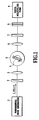
- FIG. 1 is a diagram showing a configuration for the second harmonic generation using a KLTN crystal.
- the KLTN crystal 4 is a 0.5 mm thick plate with its both surfaces optically polished. It includes electrodes formed within an incidence plane by depositing gold, and connected to a DC power supply through copper wires connected to the electrodes.
- the crystal material is composed of KTa 1-x Nb x O 3 and/or K 1-y Li y Ta 1-x Nb x O 3 .
- a fundamental wave generator 1 generates a 1.55 ⁇ m fundamental wave in accordance with to a differential frequency between an Nd:YAG Q-switched laser and an excimer laser.
- a polarizer 2 controls the polarization of the fundamental wave in the direction parallel to the electric field, and launches it between the electrodes of a KLTN crystal 4 mounted on a rotary stage 5 via a lens 3.
- the KLTN crystal 4 rotating on an axis in the direction of the electric field, causes the SHG (Second Harmonic Generation) light to pass through a polarizer 7 via a lens 6.
- the SHG light passes through a filter 8 so that only the light with the same polarization direction as that of the incident light is launched into a photo multiplier tube 8.
- FIG. 2 illustrates its result.
- a denotes the second harmonic from the KLTN crystal of the present embodiment 1
- b denotes the second harmonic from the LN used as a standard sample.
- FIG. 2 clearly shows that the KLTN crystal supplied with the electric field generates the SHG light a , and that the crystal comes to have the wavelength conversion function by the electric field applied thereto.
- the angle dependence of the SHG light intensity illustrated in FIG. 2 is based on the relationship between the nonlinear coherence length of the crystal and the interaction length of the fundamental wave, the peak interval of which allows to estimate the depth of the effective electric field formed in the KLTN. In this case, it is estimated about 0.2 mm.
- the SHG intensity obtained by applying the electric field of one KV/cm is about 10 times greater than that of the LN, corresponding to about 79 pm/V in terms of a second order nonlinear coefficient. This is the greatest second order nonlinear coefficient among the nonlinear optical crystals reported up to now.
- a new electrode was formed on the surface, on which the electrodes used in the foregoing measurement were not formed, such that the two electrodes become perpendicular.
- the two electrodes were supplied with the one KV/cm electric field, and the fundamental wave was normally launched onto the two electrodes.
- the SHG light with the same intensity was observed for the two polarized waves, thereby demonstrating that the KLTN crystal can achieve the wavelength conversion of the signal light including any polarized wave by controlling the application direction of the electric fields.
- FIG. 3 illustrates the rate of change of the SHG light intensity with respect to time, which was measured by turning the electric field on and off. It is clear from FIG. 3 that the SHG light was generated by applying the electric field, and eliminated by removing it.
- the KLTN crystal functions as a transparent medium without the electric field, and as a switch capable of turning on and off the converted light by the on-off of the electric field.
- the nonlinear constant varies in proportion to the applied voltage, it is clear that the KLTN crystal operates not only as the switch, but also as a modulator capable of modulating the converted light intensity by the electric field.
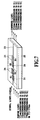
- a rectangular waveguide structure as shown in FIG. 4 was fabricated using photolithography and liquid phase epitaxial technique.
- the fabricated KLTN waveguide 13 has a refractive index difference of 2.5%, and the cutoff wavelength in a high-order mode is 0.6 ⁇ m. Thus, it functions as a single-mode waveguide for a long wavelength.
- the fabricated waveguide was 3 cm long, and the loss of the waveguide was 0.15 dB/cm.
- FIG. 4 shows a wavelength converter fabricated in this way.
- a substrate 15 was composed of SrTiO 3 doped with La, and gold was deposited on a top electrode 14.
- the period of the electrode elements corresponds to the grating period that enables the quasi-phase matching needed for the wavelength conversion of 1.55 ⁇ m band using the pumping light of 0.775 ⁇ m. In this case, the period of electrode elements becomes 12 ⁇ m.
- the outgoing light was measured using an optical spectrum analyzer with applying the voltage of one KV/cm to the electrode, and launching the 1.54 ⁇ m signal light and 0.775 ⁇ m pumping light simultaneously into the incidence edge using a polarization-maintaining optical fiber.
- FIG. 5 is a graph illustrating a spectrum after the wavelength conversion.
- the reference symbol c designates input signal light
- d designates the second-order diffraction light of the pumping light
- e designates the converted light.
- FIG. 5 clearly shows that the wavelength conversion is implemented by the differential frequency generation.
- the signal light and converted light undergo the parametric amplification, and the gain of the converted light with respect to the input signal light reaches about 15 dB, which is such a high gain that the conventional LN wavelength converter cannot achieve.
- the conversion efficiency can also be controlled by varying the intensity of the electric field applied, and it is only the signal light that is output by turning off the electric field.
- the KTN waveguide had a propensity to vary its efficiency more sensitively to temperature than the KLTN waveguide.
- a device as shown in FIG. 6 was fabricated by adding new electrodes to the wavelength converter of the foregoing embodiment 2, and an experiment similar to that of the embodiment 2 was conducted concerning the wavelength conversion.
- the reference numeral 19 designates a KLTN waveguide
- 20 designates a top electrode for TM polarization for converting a TM polarization
- 21 designates an electrode for TE polarization for converting a TE polarization
- 22 designates an La-doped SrTiO 3 used as a bottom electrode for the TM polarization and as a substrate.
- the wavelength conversion characteristics were measured for both the TE and TM polarizations this time.
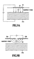
- FIGs. 9A and 9B show cross-sections of the electrodes perpendicular to the waveguide: FIG. 9A shows the placement of the electrode for the TM polarization; and FIG. 9B shows the placement of the electrode for the TE polarization.
- the reference numeral 31a designates an electrode (substrate)
- 31b designates a substrate
- 32 designates a waveguide
- reference numerals 33, 33a and 33b each designate an electrode. Since the electric field distribution differs depending on the electrode structure, the TE polarization requires about 1.5 times greater electric field than the TM polarization to obtain the same conversion efficiency between the TE and TM. However, it was easy to implement polarization insensitive wavelength conversion by adjusting the electric field applied. In addition, it was possible to implement the wavelength conversion of only one of the polarized waves by turning on and off the electric field.
- FIG. 7 shows a structure of the wavelength converter fabricated in this way.
- the reference numeral 23 designates a KLTN waveguide
- each reference numeral 24 designates a top electrode
- 25 designates an La-doped SrTiO 3 used as a bottom electrode and substrate.
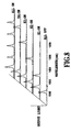
- FIG. 8 illustrates the resultant wavelength conversion spectra.
- FIG. 8 illustrates that the converted light varies its wavelength successively in accordance with the changes of the electrodes the voltages are applied to, and that it functions as a bias in the wavelength conversion in which the wavelength to be electrically converted is controlled.
- applying voltages to several types of electrodes makes it possible to convert the signal light into several wavelengths, which shows that the device is applicable as a wavelength converter for multicast and the like.
- FIG. 8 illustrates only the wavelength conversion spectra obtained by eliminating the light generated by the multiple conversion by filters.
- noise figure measurement of the wavelength conversion was conducted which was carried out by using the signal light (1.543 ⁇ m) modulated to a 160 Gbit/s signal and 0.775 ⁇ m pumping light (CW light).
- the noise figure which was measured optically and electrically, was less than 0.5 dB, with exhibiting no noise increase by the wavelength conversion.
- the present embodiment 5 can respond to a high rate signal to which the wavelength converter using the optical semiconductor cannot respond. Thus, it was demonstrated that a noise-free wavelength conversion was implemented.
- a rectangular waveguide structure was fabricated using the photolithography and liquid phase epitaxial technique.
- the fabricated waveguide has a refractive index difference of 2.5%, and the cutoff wavelength in a high-order mode is 0.6 ⁇ m. Thus, it functions as a single-mode waveguide for a long wavelength.
- the fabricated waveguide was 3 cm long, and the loss of the waveguide was 0.15 dB/cm.
- the substrate is composed of SrTiO3 doped with La, on which gold was deposited to form electrode patterns. It was also possible to form a similar wavelength converter using KTaO 3 as the substrate, and deposited Pt as the bottom electrode.
- FIG. 7 is a perspective view showing a structure of the wavelength converter as a wavelength tunable wavelength light source fabricated in the same manner as the foregoing embodiment 4.
- the device was subjected to temperature control by a Peltier device to stabilize the efficiency and signal wavelength.
- the periods of the electrodes that can implement the quasi-phase matching required for the differential frequency generation of the light with the wavelength of 1.55 ⁇ m band using the pumping light with the wavelengths of 0.770, 0.775, 0.780, and 0.785 ⁇ m. In this case, the periods of the electrode elements become 12-13 ⁇ m.
- the output was measured using an optical spectrum analyzer with applying the voltage of one KV/cm to the electrodes, and launching the 1.53 ⁇ m signal light fed from the signal light generator and the pumping light with the wavelength of 0.770, 0.775, 0.780, and 0.785 ⁇ m fed from the pumping light generator simultaneously into the incidence end using a polarization-maintaining optical fiber.
- FIG. 8 is a graph illustrating spectra generated by applying the electric field sequentially to the electrodes as described above.
- FIG. 8 clearly shows that the wavelength tunable light source is implemented by the differential frequency generation.
- the signal light and converted light undergo the parametric amplification, and the gain of the converted light with respect to the input signal light reaches about 15 dB, which is a high gain the conventional LN wavelength converter cannot achieve.
- the conversion efficiency can also be controlled by varying the intensity of the electric field applied, and it is only the signal light that is output by turning off the electric field.
- the wavelength converter could also maintain the intensity of the output light at nearly the fixed value by operating it in the gain saturation region.
- the output light intensity could be maintained at a fixed value by applying progressively strong electric field as the electrodes approached the output side.
- FIG. 7 shows a configuration in which the electrode surfaces 24 and 25 are disposed in the vertical direction.
- the TE and TM polarizations can be generated independently by disposing, besides the electrodes disposed in the vertical direction, electrodes in the direction horizontal to the surface, and by supplying the horizontal electrodes with electric field independently of the vertical electrodes.
- FIGs. 9A and 9B are cross-sectional views showing planar optical waveguide in accordance with the present invention, which is sectioned normally to the waveguide at the positions of the electrodes.
- FIG. 9A shows a structure that disposes the electrode surfaces 31a and 33 in the vertical direction
- FIG. 9B shows a structure that disposes the electrode surfaces 33a and 33b in the horizontal direction.
- the electric field modulated by 10 GHz was sequentially applied to the electrodes.
- a light signal modulated by 10 GHz can be obtained as the need arises.
- the channel spacing can be readily varied by controlling the periods of the electrode elements, that is, by making phase matching between the wavelength of the pumping light and the wavelength of the signal light.
- the signal light of 1530 nm consists of a pulse train of 100 GHz of a fiber-ring laser, the variable wavelength light source can also generate the signal light of 100 Gbit/s.
- the wavelength tunable light source covering a 1250-1700 nm range was easily implemented by disposing chips with different electrode patterns in parallel.
- the number of the wavelengths was increased in the same method as the embodiment 6 except that the present embodiment 8 used the pumping light with 767.75, 774.75, 784.75 and 804.75 nm, and signal light including 10 wavelengths of 1528, 1529, 1530, 1531, 1532, 1533, 1534, 1535, 1536 and 1537 nm as the light launched into the multi-wavelength light source, thereby implementing a multiple wavelength scheme.
- FIG. 10 shows the wavelengths obtained by applying the electric fields to the electrode as required. As shown in FIG. 10, when the electrodes are each turned on, the signal with the wavelength corresponding to the differential frequency is obtained. Accordingly, applying the electric fields to each electrode makes it possible to double the number wavelengths.
- the signal light passing through the four stages of the electrodes will include the total of 160 waves.
- applying the present invention can implement a multi-wavelength light source by a single-chip device with ease. It is obvious that connecting chips, each including one electrode, by fibers can also implement a similar light source.
- selecting the electrode to which the electric field is applied makes it possible to obtain a signal including a necessary number of wavelengths in a required wavelength range.
- the initially incident 10 wavelengths which were launched into the foregoing embodiment 8 of the multi-wavelength light source, were generated by the multi-wavelength light source with the same structure as the embodiment 6 including 10 types of electrodes.
- an experiment similar to that of embodiment 8 was conducted using a 100 GHz pulse train of a fiber-ring laser or semiconductor mode-locking laser as the initial signal light among them.
- all the resultant wavelengths were the same as those of the foregoing embodiment 8, all the signals were composed of short pulses modulated by 100 GHz.
- the method in accordance with the present invention has an advantage of being able to generate the signal light with multiple wavelengths consisting of short pulses easily.
- the temperature of the waveguide with the electrodes which was fabricated by the same method as the foregoing embodiments, was dropped with applying electric field.
- the phase transition temperature of the KLTN crystal constituting the core was 5°C, and the waveguide was cooled down to -10°C, followed by removing the application of the electric field.
- the wavelength conversion was carried out in the same method as the foregoing embodiments.
- the electric field was not applied, the foregoing wavelength conversion efficiency was achieved. This is because the temperature drop caused the crystal to transition from the cubic system to the tetragonal system, and the electric field due to spontaneous polarization generated in the crystal brought about the secondary nonlinear effect in place of the external electrodes.
- phase transition temperature of the crystal can be controlled by varying the composition ratio of Nb and Ta. Accordingly, the design becomes possible of the wavelength converter that will minimize the power consumption of the temperature control near the room temperature by selecting the composition depending on whether the electric field application precedes, or the operation is fixed to that does not induce the electric field.
- a wavelength converter implements high speed, high efficiency, low noise wavelength conversion without performing high voltage poling of a crystal, and enables switching and modulation of converted light in response to an electric field.
- a KLTN crystal (4) which is a 0.5 mm thick plate with its surfaces optically polished, includes a deposited-gold electrode within its incidence plane, and is connected to a DC power supply via a copper wire.
- the crystal material is composed of KTa 1-x Nb x O 3 and/or K 1-y Li y Ta 1-x Nb x O 3 .
- a fundamental wave generator (1) generates a 1.55 ⁇ m fundamental wave in accordance with a differential frequency between an Nd:YAG Q-switched laser and an excimer laser.
- a polarizer (2) controls the polarization of the fundamental wave in the direction parallel to the electric field, and launches it into the electrode of the KLTN crystal (4).
- the KLTN crystal (4) rotating on an axis in the direction of the electric field, launches only part of the generated SHG light with the same polarization direction as that of the incident light into a photo multiplier tube (8) through a polarizer (7).
Landscapes
- Physics & Mathematics (AREA)
- Nonlinear Science (AREA)
- General Physics & Mathematics (AREA)
- Optics & Photonics (AREA)
- Chemical & Material Sciences (AREA)
- Crystallography & Structural Chemistry (AREA)
- Optical Modulation, Optical Deflection, Nonlinear Optics, Optical Demodulation, Optical Logic Elements (AREA)
- Lasers (AREA)
Abstract
Description
Claims (42)
- A wavelength converter for producing converted light with a wavelength corresponding to an energy difference between signal light and pumping light with a wavelength different from that of the signal light, by launching the signal light and the pumping light into a crystal material simultaneously, wherein said crystal material consists of a crystal composed of at least one of KTa1-xNbxO3 and K1-yLiyTa1-xNbxO3.
- The wavelength converter as claimed in claim 1, wherein said crystal material is supplied with an electric field to induce wavelength conversion.
- The wavelength converter as claimed in claim 2, wherein said crystal material comprises a comb electrode with an electrode period that will establish quasi-phase matching between the signal light and the pumping light.
- The wavelength converter as claimed in claim 2, wherein said electrode comprises at least two electrodes with different periods.
- The wavelength converter as claimed in claim 2, wherein said crystal material comprises an electrode structure that enables the electric field to be applied to said electrode structure in at least two directions.
- The wavelength converter as claimed in claim 2, wherein said crystal material comprises a core with a high refractive index and a cladding with a low refractive index, both of them being composed of at least one of KTa1-xNbxO3 and K1-yLiyTa1-xNbxO3 with different compositions.
- The wavelength converter as claimed in claim 2, further comprising an application halting means for halting applying the electric field when a temperature of a waveguide is dropped below a phase transition temperature with applying the electric field, wherein said wavelength converter carries out wavelength conversion after said application halting means halts applying the electric field.
- The wavelength converter as claimed in claim 1, wherein the converted light is modulated by modulating the electric field applied to said crystal material.
- The wavelength converter as claimed in claim 8, wherein said crystal material comprises a comb electrode with an electrode period that will establish quasi-phase matching between the signal light and the pumping light.
- The wavelength converter as claimed in claim 8, wherein said electrode comprises at least two electrodes with different periods.
- The wavelength converter as claimed in claim 8, wherein said crystal material comprises an electrode structure that enables the electric field to be applied to said electrode structure in at least two directions.
- The wavelength converter as claimed in claim 8, wherein said crystal material comprises a core with a high refractive index and a cladding with a low refractive index, both of them being composed of at least one of KTa1-xNbxO3 and K1-yLiyTa1-xNbxO3 with different compositions.
- The wavelength converter as claimed in claim 8, further comprising an application halting means for halting applying the electric field when a temperature of a waveguide is dropped below a phase transition temperature with applying the electric field, wherein said wavelength converter carries out wavelength conversion after said application halting means halts applying the electric field.
- The wavelength converter as claimed in claim 1, wherein said crystal material comprises a comb electrode with an electrode period that will establish quasi-phase matching between the signal light and the pumping light.
- The wavelength converter as claimed in claim 14, wherein said electrode comprises at least two electrodes with different periods.
- The wavelength converter as claimed in claim 14, wherein said crystal material comprises an electrode structure that enables the electric field to be applied to said electrode structure in at least two directions.
- The wavelength converter as claimed in claim 14, wherein said crystal material comprises a core with a high refractive index and a cladding with a low refractive index, both of them being composed of at least one of KTa1-xNbxO3 and K1-yLiyTa1-xNbxO3 with different compositions.
- The wavelength converter as claimed in claim 14, further comprising an application halting means for halting applying the electric field when a temperature of a waveguide is dropped below a phase transition temperature with applying the electric field, wherein said wavelength converter carries out wavelength conversion after said application halting means halts applying the electric field.
- The wavelength converter as claimed in claim 1, wherein said electrode comprises at least two electrodes with different periods.
- The wavelength converter as claimed in claim 19, wherein said crystal material comprises a core with a high refractive index and a cladding with a low refractive index, both of them being composed of at least one of KTa1-xNbxO3 and K1-yLiyTa1-xNbxO3 with different compositions.
- The wavelength converter as claimed in claim 19, further comprising an application halting means for halting applying the electric field when a temperature of a waveguide is dropped below a phase transition temperature with applying the electric field, wherein said wavelength converter carries out wavelength conversion after said application halting means halts applying the electric field.
- The wavelength converter as claimed in claim 1, wherein said crystal material comprises an electrode structure that enables the electric field to be applied to said electrode structure in at least two directions.
- The wavelength converter as claimed in claim 22, further comprising an application halting means for halting applying the electric field when a temperature of a waveguide is dropped below a phase transition temperature with applying the electric field, wherein said wavelength converter carries out wavelength conversion after said application halting means halts applying the electric field.
- The wavelength converter as claimed in claim 1, wherein said crystal material comprises a core with a high refractive index and a cladding with a low refractive index, both of them being composed of at least one of KTa1-xNbxO3 and K1-yLiyTa1-xNbxO3 with different compositions.
- The wavelength converter as claimed in claim 24, further comprising an application halting means for halting applying the electric field when a temperature of a waveguide is dropped below a phase transition temperature with applying the electric field, wherein said wavelength converter carries out wavelength conversion after said application halting means halts applying the electric field.
- The wavelength converter as claimed in claim 1, further comprising an application halting means for halting applying the electric field when a temperature of a waveguide is dropped below a phase transition temperature with applying the electric field, wherein said wavelength converter carries out wavelength conversion after said application halting means halts applying the electric field.
- A wavelength converter operating as a multi-wavelength light source including a planar optical waveguide comprising:a core with a high refractive index composed of a crystal material with a composition of at least one of KTa1-xNbxO3 and K1-yLiyTa1-xNbxO3 ;a cladding surrounding said core;an electrode that is formed on a surface of said optical waveguide and has a fixed electrode period;signal light generating means for generating signal light with at least one wavelength; andpumping light generating means for generating pumping light with a wavelength different from that of the signal light output from said signal light generating means, whereinthe signal light and the pumping light are launched simultaneously into said optical waveguide to generate signal light with at least one wavelength.
- The wavelength converter as claimed in claim 27, wherein the electrode period satisfies quasi-phase matching condition required for differential frequency generation based on an energy difference between the signal light and the pumping light.
- The wavelength converter as claimed in claim 28, wherein said electrode has a structure that enables the electric field to be applied in at least one of two directions parallel to a direction of an electric field of TE polarization of the signal light and parallel to a direction of TM polarization of the signal light.
- The wavelength converter as claimed in claim 28, wherein the signal light is modulated by modulating a voltage applied to said electrode.
- The wavelength converter as claimed in claim 28, wherein said electrode comprises a plurality of electrodes with different periods.
- The wavelength converter as claimed in claim 28, further comprising an application halting means for halting applying the electric field when a temperature of a waveguide is dropped below a phase transition temperature with applying the electric field, wherein said wavelength converter carries out wavelength conversion after said application halting means halts applying the electric field.
- The wavelength converter as claimed in claim 27, wherein said electrode has a structure that enables the electric field to be applied in at least one of two directions parallel to a direction of an electric field of TE polarization of the signal light and parallel to a direction of TM polarization of the signal light.
- The wavelength converter as claimed in claim 33, wherein the signal light is modulated by modulating a voltage applied to said electrode.
- The wavelength converter as claimed in claim 33, wherein said electrode comprises a plurality of electrodes with different periods.
- The wavelength converter as claimed in claim 33, further comprising an application halting means for halting applying the electric field when a temperature of a waveguide is dropped below a phase transition temperature with applying the electric field, wherein said wavelength converter carries out wavelength conversion after said application halting means halts applying the electric field.
- The wavelength converter as claimed in claim 27, wherein the signal light is modulated by modulating a voltage applied to said electrode.
- The wavelength converter as claimed in claim 37, wherein said electrode comprises a plurality of electrodes with different periods.
- The wavelength converter as claimed in claim 37, further comprising an application halting means for halting applying the electric field when a temperature of a waveguide is dropped below a phase transition temperature with applying the electric field, wherein said wavelength converter carries out wavelength conversion after said application halting means halts applying the electric field.
- The wavelength converter as claimed in claim 27, wherein said electrode comprises a plurality of electrodes with different periods.
- The wavelength converter as claimed in claim 40, further comprising an application halting means for halting applying the electric field when a temperature of a waveguide is dropped below a phase transition temperature with applying the electric field, wherein said wavelength converter carries out wavelength conversion after said application halting means halts applying the electric field.
- The wavelength converter as claimed in claim 27, further comprising an application halting means for halting applying the electric field when a temperature of a waveguide is dropped below a phase transition temperature with applying the electric field, wherein said wavelength converter carries out wavelength conversion after said application halting means halts applying the electric field.
Applications Claiming Priority (4)
| Application Number | Priority Date | Filing Date | Title |
|---|---|---|---|
| JP2001103552A JP3623749B2 (en) | 2001-04-02 | 2001-04-02 | Wavelength conversion device |
| JP2001103552 | 2001-04-02 | ||
| JP2001104943A JP3623750B2 (en) | 2001-04-03 | 2001-04-03 | Multi-wavelength light source |
| JP2001104943 | 2001-04-03 |
Publications (2)
| Publication Number | Publication Date |
|---|---|
| EP1248143A2 true EP1248143A2 (en) | 2002-10-09 |
| EP1248143A3 EP1248143A3 (en) | 2004-10-20 |
Family
ID=26612969
Family Applications (1)
| Application Number | Title | Priority Date | Filing Date |
|---|---|---|---|
| EP02007153A Withdrawn EP1248143A3 (en) | 2001-04-02 | 2002-03-28 | Wavelength converter |
Country Status (2)
| Country | Link |
|---|---|
| US (1) | US6795232B2 (en) |
| EP (1) | EP1248143A3 (en) |
Cited By (3)
| Publication number | Priority date | Publication date | Assignee | Title |
|---|---|---|---|---|
| WO2005008304A1 (en) * | 2003-07-16 | 2005-01-27 | Nippon Telegraph And Telephone Corporation | Optical waveguide material and optical waveguide |
| WO2005124398A1 (en) | 2004-06-22 | 2005-12-29 | Nippon Telegraph And Telephone Corporation | Optical material, optical lens and prism |
| WO2017125691A1 (en) * | 2016-01-22 | 2017-07-27 | Centre National De La Recherche Scientifique - Cnrs - | Device for generating a polychromatic and spatially self-adapted beam of photons |
Families Citing this family (7)
| Publication number | Priority date | Publication date | Assignee | Title |
|---|---|---|---|---|
| US6862130B2 (en) * | 2001-01-08 | 2005-03-01 | Lightbit Corporation, Inc. | Polarization-insensitive integrated wavelength converter |
| JP2003188455A (en) * | 2001-12-18 | 2003-07-04 | Matsushita Electric Ind Co Ltd | Single wavelength laser module |
| KR100888299B1 (en) * | 2003-03-19 | 2009-03-11 | 니폰덴신뎅와 가부시키가이샤 | Optical switch |
| US8509582B2 (en) * | 2005-08-30 | 2013-08-13 | Rambus Delaware Llc | Reducing light leakage and improving contrast ratio performance in FTIR display devices |
| KR100826436B1 (en) * | 2006-11-03 | 2008-04-29 | 삼성전기주식회사 | Wavelength conversion laser device |
| KR100988471B1 (en) * | 2007-07-06 | 2010-10-18 | 전자부품연구원 | Real-time cell analysis device and measuring method of cell metabolism using same |
| US8508841B2 (en) * | 2011-03-04 | 2013-08-13 | HC Photonic Corp. | Light conversion module and light source system including the same |
Family Cites Families (20)
| Publication number | Priority date | Publication date | Assignee | Title |
|---|---|---|---|---|
| US3293557A (en) * | 1964-03-19 | 1966-12-20 | Bell Telephone Labor Inc | Elastic wave devices utilizing mixed crystals of potassium tantalatepotassium niobate |
| US3328723A (en) * | 1965-12-23 | 1967-06-27 | Bell Telephone Labor Inc | Optical frequency parametric oscillators and modulators with temperature and electrical control |
| US3430061A (en) * | 1967-11-24 | 1969-02-25 | Bell Telephone Labor Inc | Solid state waveguide optical second harmonic generator |
| US3746879A (en) * | 1972-05-25 | 1973-07-17 | Ibm | Superlattice harmonic generator & mixer for electromagnetic waves |
| FR2385114A1 (en) * | 1977-03-23 | 1978-10-20 | Thomson Csf | THIN-LAYER NON-LINEAR OPTICAL DEVICE AND ITS MANUFACTURING PROCESS |
| GB8803450D0 (en) * | 1988-02-15 | 1988-03-16 | British Telecomm | Optical frequency mixer |
| JPH05333395A (en) * | 1992-04-03 | 1993-12-17 | Fuji Photo Film Co Ltd | Optical wavelength conversion device |
| JPH06110095A (en) * | 1992-09-28 | 1994-04-22 | Hiromasa Ito | Method and device for generating millimeter wave and submillimeter wave |
| US5317666A (en) * | 1992-09-29 | 1994-05-31 | Eastman Kodak Company | Waveguide nonlinear optical frequency converter with integral modulation and optimization means |
| JP3443889B2 (en) * | 1993-09-10 | 2003-09-08 | ソニー株式会社 | Local polarization control method for nonlinear optical materials |
| US5434700A (en) * | 1993-12-16 | 1995-07-18 | Bell Communications Research, Inc. | All-optical wavelength converter |
| JPH08510571A (en) * | 1994-03-11 | 1996-11-05 | フィリップス エレクトロニクス ネムローゼ フェンノートシャップ | Equipment for increasing the frequency of electromagnetic radiation |
| JPH08160476A (en) * | 1994-12-06 | 1996-06-21 | Oki Electric Ind Co Ltd | Optical wavelength conversion element |
| JP3616181B2 (en) * | 1995-10-26 | 2005-02-02 | 弘昌 伊藤 | Optical device |
| US5644422A (en) * | 1996-01-16 | 1997-07-01 | New Focus, Inc. | Techniques of radiation phase matching within optical crystals |
| US5912910A (en) * | 1996-05-17 | 1999-06-15 | Sdl, Inc. | High power pumped mid-IR wavelength systems using nonlinear frequency mixing (NFM) devices |
| US6002515A (en) * | 1997-01-14 | 1999-12-14 | Matsushita Electric Industrial Co., Ltd. | Method for producing polarization inversion part, optical wavelength conversion element using the same, and optical waveguide |
| JP3681893B2 (en) * | 1998-03-20 | 2005-08-10 | パイオニア株式会社 | Wavelength conversion element and method for manufacturing wavelength conversion element |
| JP2000066254A (en) * | 1998-08-18 | 2000-03-03 | Matsushita Electric Ind Co Ltd | Method of forming domain-inverted structure |
| US6542285B1 (en) * | 1998-12-14 | 2003-04-01 | The Board Of Trustees Of The Leland Stanford Junior University | Backswitch poling method for domain patterning of ferroelectric materials |
-
2002
- 2002-03-28 EP EP02007153A patent/EP1248143A3/en not_active Withdrawn
- 2002-03-29 US US10/108,996 patent/US6795232B2/en not_active Expired - Fee Related
Cited By (11)
| Publication number | Priority date | Publication date | Assignee | Title |
|---|---|---|---|---|
| WO2005008304A1 (en) * | 2003-07-16 | 2005-01-27 | Nippon Telegraph And Telephone Corporation | Optical waveguide material and optical waveguide |
| US7177514B2 (en) | 2003-07-16 | 2007-02-13 | Nippon Telegraph And Telephone Corporation | Optical waveguide material and optical waveguide |
| CN100353193C (en) * | 2003-07-16 | 2007-12-05 | 日本电信电话株式会社 | Optical waveguide material and optical waveguide |
| US7340147B2 (en) | 2003-07-16 | 2008-03-04 | Nippon Telegraph And Telephone Corporation | Optical waveguide material and optical waveguide |
| EP2312351A1 (en) * | 2003-07-16 | 2011-04-20 | Nippon Telegraph And Telephone Corporation | Optical waveguide material and optical waveguide |
| WO2005124398A1 (en) | 2004-06-22 | 2005-12-29 | Nippon Telegraph And Telephone Corporation | Optical material, optical lens and prism |
| WO2017125691A1 (en) * | 2016-01-22 | 2017-07-27 | Centre National De La Recherche Scientifique - Cnrs - | Device for generating a polychromatic and spatially self-adapted beam of photons |
| FR3047118A1 (en) * | 2016-01-22 | 2017-07-28 | Centre Nat De La Rech Scient - Cnrs - | DEVICE FOR GENERATING A POLYCHROMATIC AND SPATIALLY SELF-ADAPTED PHOTON BEAM |
| CN109154760A (en) * | 2016-01-22 | 2019-01-04 | 国立科学研究中心 | Device for generating polychromatic and spatially adaptive photonic beams |
| US10718991B2 (en) | 2016-01-22 | 2020-07-21 | Centre National De La Recherche Scientifique | Device for generating a polychromatic and spatially self-adapted beam of photons |
| CN109154760B (en) * | 2016-01-22 | 2021-11-02 | 国立科学研究中心 | Device for generating polychromatic and spatially adaptive photonic beams |
Also Published As
| Publication number | Publication date |
|---|---|
| US6795232B2 (en) | 2004-09-21 |
| US20020141040A1 (en) | 2002-10-03 |
| EP1248143A3 (en) | 2004-10-20 |
Similar Documents
| Publication | Publication Date | Title |
|---|---|---|
| Chou et al. | 1.5-μm-band wavelength conversion based on cascaded second-order nonlinearity in LiNbO 3 waveguides | |
| Sohler et al. | Integrated optical devices in lithium niobate | |
| Murata et al. | Optical pulse generation by electrooptic-modulation method and its application to integrated ultrashort pulse generators | |
| Rabiei et al. | Tunable polymer double micro-ring filters | |
| US7315697B2 (en) | Light source for generating an output signal having spaced apart frequencies | |
| WO2003028264A2 (en) | Light source for generating an output signal having spaced apart frequencies | |
| US6795232B2 (en) | Wavelength converter | |
| RU2200970C2 (en) | Electrically tunable optical filter | |
| JP3792638B2 (en) | Wavelength range of nonlinear optics increased by nonuniformly chirped quasi-phase matching | |
| KR20010013957A (en) | Method and apparatus for switching, amplification, control and modulation | |
| Shumakher et al. | Optoelectronic oscillator tunable by an SOA based slow light element | |
| Asobe et al. | Wavelength conversion using quasi-phase matched LiNbO 3 waveguides | |
| Sohler et al. | Frequency Conversion In Ti: LiNbO [sub] 3 [/sub] Optical Waveguides | |
| JP4636527B2 (en) | Optical frequency comb generator and multi-wavelength light source using the same | |
| US6584260B2 (en) | Electro-optical device and a wavelength selection method utilizing the same | |
| Yao et al. | Investigation of room-temperature multiwavelength fiber-ring laser that incorporates an SOA-based phase modulator in the laser cavity | |
| WO2004107033A1 (en) | Frequency comb generator | |
| CN1490658A (en) | Difference frequency all-optical wavelength converter | |
| CN1329773C (en) | Wavelength changing element and use thereof | |
| JP3623750B2 (en) | Multi-wavelength light source | |
| JP3623749B2 (en) | Wavelength conversion device | |
| US6856450B2 (en) | Method and apparatus for generating a sequence of optical wavelength bands | |
| Qasymeh et al. | Frequency-tunable microwave generation based on time-delayed optical combs | |
| Lu et al. | Application of periodically-poled LiNbO/sub 3/for wide-bandwidth high-frequency electrooptic modulator | |
| Wen et al. | Broadband Flat-Top Electro-Optic Frequency Comb Generation Based on Integrated Thin-Film Lithium Niobate Modulators |
Legal Events
| Date | Code | Title | Description |
|---|---|---|---|
| PUAI | Public reference made under article 153(3) epc to a published international application that has entered the european phase |
Free format text: ORIGINAL CODE: 0009012 |
|
| 17P | Request for examination filed |
Effective date: 20020328 |
|
| AK | Designated contracting states |
Kind code of ref document: A2 Designated state(s): AT BE CH CY DE DK ES FI FR GB GR IE IT LI LU MC NL PT SE TR |
|
| AX | Request for extension of the european patent |
Free format text: AL;LT;LV;MK;RO;SI |
|
| PUAL | Search report despatched |
Free format text: ORIGINAL CODE: 0009013 |
|
| AK | Designated contracting states |
Kind code of ref document: A3 Designated state(s): AT BE CH CY DE DK ES FI FR GB GR IE IT LI LU MC NL PT SE TR |
|
| AX | Request for extension of the european patent |
Extension state: AL LT LV MK RO SI |
|
| RIC1 | Information provided on ipc code assigned before grant |
Ipc: 7G 02F 1/355 B Ipc: 7G 02F 1/35 B Ipc: 7G 02F 1/365 B Ipc: 7G 02F 1/335 B Ipc: 7G 02F 1/39 A |
|
| AKX | Designation fees paid |
Designated state(s): DE FR GB IT |
|
| STAA | Information on the status of an ep patent application or granted ep patent |
Free format text: STATUS: THE APPLICATION IS DEEMED TO BE WITHDRAWN |
|
| 18D | Application deemed to be withdrawn |
Effective date: 20121002 |