EP1246420A2 - Failsafe detection system and method for differential receivers - Google Patents
Failsafe detection system and method for differential receivers Download PDFInfo
- Publication number
- EP1246420A2 EP1246420A2 EP02100302A EP02100302A EP1246420A2 EP 1246420 A2 EP1246420 A2 EP 1246420A2 EP 02100302 A EP02100302 A EP 02100302A EP 02100302 A EP02100302 A EP 02100302A EP 1246420 A2 EP1246420 A2 EP 1246420A2
- Authority
- EP
- European Patent Office
- Prior art keywords
- failsafe
- signal
- indicator
- timer
- gate
- Prior art date
- Legal status (The legal status is an assumption and is not a legal conclusion. Google has not performed a legal analysis and makes no representation as to the accuracy of the status listed.)
- Granted
Links
- 238000001514 detection method Methods 0.000 title claims abstract description 18
- 238000000034 method Methods 0.000 title claims abstract description 17
- 230000007704 transition Effects 0.000 claims abstract description 28
- 230000000694 effects Effects 0.000 claims abstract description 25
- 230000004913 activation Effects 0.000 claims abstract description 4
- 230000004044 response Effects 0.000 claims description 3
- 230000003213 activating effect Effects 0.000 claims 1
- 230000008878 coupling Effects 0.000 claims 1
- 238000010168 coupling process Methods 0.000 claims 1
- 238000005859 coupling reaction Methods 0.000 claims 1
- 230000009849 deactivation Effects 0.000 claims 1
- 230000011664 signaling Effects 0.000 description 7
- 230000005540 biological transmission Effects 0.000 description 4
- 238000010586 diagram Methods 0.000 description 3
- 230000008859 change Effects 0.000 description 2
- 238000004088 simulation Methods 0.000 description 2
- UPLPHRJJTCUQAY-WIRWPRASSA-N 2,3-thioepoxy madol Chemical compound C([C@@H]1CC2)[C@@H]3S[C@@H]3C[C@]1(C)[C@@H]1[C@@H]2[C@@H]2CC[C@](C)(O)[C@@]2(C)CC1 UPLPHRJJTCUQAY-WIRWPRASSA-N 0.000 description 1
- 230000003321 amplification Effects 0.000 description 1
- 238000006243 chemical reaction Methods 0.000 description 1
- 230000003111 delayed effect Effects 0.000 description 1
- 230000004048 modification Effects 0.000 description 1
- 238000012986 modification Methods 0.000 description 1
- 238000003199 nucleic acid amplification method Methods 0.000 description 1
- 230000002028 premature Effects 0.000 description 1
- 230000008707 rearrangement Effects 0.000 description 1
- 238000006467 substitution reaction Methods 0.000 description 1
Images


Classifications
-
- H—ELECTRICITY
- H03—ELECTRONIC CIRCUITRY
- H03K—PULSE TECHNIQUE
- H03K19/00—Logic circuits, i.e. having at least two inputs acting on one output; Inverting circuits
- H03K19/007—Fail-safe circuits
-
- H—ELECTRICITY
- H04—ELECTRIC COMMUNICATION TECHNIQUE
- H04L—TRANSMISSION OF DIGITAL INFORMATION, e.g. TELEGRAPHIC COMMUNICATION
- H04L25/00—Baseband systems
- H04L25/02—Details ; arrangements for supplying electrical power along data transmission lines
- H04L25/08—Modifications for reducing interference; Modifications for reducing effects due to line faults ; Receiver end arrangements for detecting or overcoming line faults
Definitions
- differential signaling technology For data transmission it is important to have bus drivers and bus receivers that allow devices to communicate quickly, efficiently, and accurately. This data transmission may occur within a computer system, for example.
- One common technique for implementation of data transmission within a computer bus uses differential signaling technology to communicate between devices in a computer system.
- Typical receiver architectures use one or more stages of low-gain/high-speed NPN input differential amplifiers to amplify an input signal, then a differential to single-ended converter stage to achieve rail-to-rail levels.
- Figure 1 illustrates the basic differential input stage architecture.
- the activity timer 230 monitors activity on the bus by taking the timer reset signal, from the circuit of Figure 1, as an input, and resets after a valid signal transition. In this way, the time required for invalid data to exist on the bus before a failsafe signal is issued can be set to a predetermined value. While there is bus activity of sufficient amplitude to drive the differential to single ended converter rail-to-rail, the output of the activity timer 230 is high. After activity has stopped, the activity timer 230 issues a low after a preset timeout period. After the activity timer 230 has gone low, the failsafe signal may go low (failsafe is active low) if a failsafe condition exists (NAND gate 220 output low) on the bus pins.
- FIG. 4 there is illustrated an invalid failsafe event which occurs when using the failsafe circuit arrangement of Figure 2.
- inputs 410, 420 have been in a valid state above the receiver threshold for a period of time longer than the activity timeout period.
- a 10nS noise spike on signal 420 causes a failsafe threshold detection followed by a failsafe (250) glitch low because the timeout period has expired.
- the receiver output would have changed states without any valid data change on the input. Further, the receiver output can oscillate as noise dissipates and re-emerges.
- a signal is enabled as an input to the timer, thus, resetting the timeout period 540.
- a failsafe bit or flag is set for a failsafe condition determined to persist subsequent to a timeout period. The failsafe bit or flag can then be used by the differential receiver to deal with the fault condition in a manner appropriate for the specific application.
- the aforementioned method can be enabled in software, hardware or a combination of both.
- comparators 205, 210 are used to detect differential voltage created by offset voltage resistors of a differential receiver device, such as R3 and R4 of Figure 1.
- the output of NAND gate 220 is high when there is valid data on the bus and low when the data signal is below a predetermined failsafe threshold. However, the output of the NAND gate 220 is delayed to OR gate 240 by a predetermined period.
- the delay device 650 is built into the OR gate input to keep a glitch or premature toggle from occurring when failsafe is detected. If the delay device 650 were not present, the failsafe condition would be transmitted through the OR gate 240 to the Failsafe bit at 660 before the activity timer 230 is reset, causing the glitch.
Landscapes
- Engineering & Computer Science (AREA)
- Power Engineering (AREA)
- Computer Networks & Wireless Communication (AREA)
- Signal Processing (AREA)
- Physics & Mathematics (AREA)
- Computer Hardware Design (AREA)
- Computing Systems (AREA)
- General Engineering & Computer Science (AREA)
- Mathematical Physics (AREA)
- Dc Digital Transmission (AREA)
- Logic Circuits (AREA)
- Small-Scale Networks (AREA)
Abstract
Description
- The present invention relates generally to the field of integrated circuits and, more particularly, to a method, system and apparatus of failsafe detection for differential receiver circuits.
- For data transmission it is important to have bus drivers and bus receivers that allow devices to communicate quickly, efficiently, and accurately. This data transmission may occur within a computer system, for example. One common technique for implementation of data transmission within a computer bus uses differential signaling technology to communicate between devices in a computer system. A variety of differential signaling standards exist, such as low voltage differential signaling (LVDS), high voltage differential signaling (HVDS) and others. Of course, such differential signaling may also be used for other long distance data transmission.
- Typically, a LVDS driver includes a current source that drives the differential pair lines in opposition to each other. The differential receiver has a high DC impedance, so that the majority of driver current flows across a termination resistor generating a voltage drop across the receiver input. When the driver switches, it changes the direction of current flow across the resistor, thereby creating a valid "1" or "0" logic state. To help ensure reliability, differential receivers may have a failsafe feature that helps to insure the output to be in a known logic state under certain fault conditions. These fault conditions can include open, shorted, or terminated receiver input.
- In interface circuits, and receiver circuits in general, it is advantageous to be able to detect failure conditions on the bus and react appropriately. Open circuit faults in general can cause problems in interface systems, sending receivers into unknown or oscillating states and generally causing havoc in digital systems. Failsafe circuits seek to detect such fault conditions and reactively apply a known state to the receiver outputs. It is also desirable that such failsafe detection circuits be capable of signaling or setting a fault bit so that digital circuits may deal with the fault conditions in a manner appropriate for the specific application.
- Although current failsafe circuits are capable of accurately detecting/signaling on occurrence of the aforementioned fault conditions, they also signal false alarms in certain signal noise related events leading to uncertainty in the state of the receiver output.
- The present invention achieves technical advantages as a method, system and apparatus for providing failsafe detection for a differential receiver. A bus activity signal is activated when receiving a differential data signal of sufficient amplitude to transition through a predetermined threshold. A failsafe signal is activated when a low differential voltage condition is detected. A countdown time period commences upon activation of either signal, and a failsafe condition is determined to exist if the failsafe signal is active when the countdown time period expires.
- For a more complete understanding of the present invention, reference is made to the following detailed description taken in conjunction with the accompanying drawings wherein:
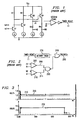
- Figure 1 illustrates a differential input stage circuit;
- Figure 2 illustrates a simple circuit diagram of a failsafe type circuit used with the input stage circuit of Figure 1;
- Figure 3 shows a graphical representation of an operation result of the failsafe type circuit shown in Figure 2;
- Figure 4 shows a graphical representation of an invalid failsafe event which can occur when using the failsafe type circuit of Figure 2;
- Figure 5 illustrates a method flow chart for failsafe detection in accordance with an embodiment of the present invention;
- Figure 6 illustrates a failsafe circuit in accordance with an embodiment of the present invention;
- Figure 7 shows a graphical representation of the output of the failsafe circuit shown in Figure 6; and
- Figure 8 illustrates exemplary operations which can be performed by the embodiment of Figure 6.
-
- The numerous innovative teachings of the present application will be described with particular reference to the presently preferred exemplary embodiments. However, it should be understood that this class of embodiments provides only a few examples of the many advantageous uses and innovative teachings herein. In general, statements made in the specification of the present application do not necessarily delimit any of the various claimed inventions. Moreover, some statements may apply to some inventive features, but not to others.
- Typical receiver architectures use one or more stages of low-gain/high-speed NPN input differential amplifiers to amplify an input signal, then a differential to single-ended converter stage to achieve rail-to-rail levels. Figure 1 illustrates the basic differential input stage architecture.
- Referring to Figure 1, the differential pair Q1 and Q2 provide gain to the input signal at In1/In2. The emitters of Q1 and Q2 are respectively coupled to Vcc via resistors R1 and R2. Q3 and Q4 are connected as emitter followers, and act as level shifters to the input of the second stage. The level-shifted signal is taken from points A1/B1 to the input of the second stage. Resistors R3 and R4 create offset voltages which are proportional to the differential input voltage. These voltages are used as inputs to a failsafe circuit. The second stage may include another amplification stage and a differential to single-ended converter, or may go directly to single ended conversion. After rail to rail levels are achieved, the second stage output goes directly into logic level gates as shown. A
Timer Reset signal 11 is created from the logic level output of the receiver. The basic concept of the existing type failsafe circuit is to use window comparators to detect low differential voltage conditions on A1/B2 and B1/A2, and to use the Timer Reset signal to indicate bus activity. - Referring now to Figure 2 there is illustrated a simple circuit diagram of an existing failsafe type circuit that can be used with the input stage architecture shown in Figure 1.
- In this circuit,
window comparators window comparators NAND gate 220, therefore, is high when there is valid data on the bus, and low when the data signal is below the failsafe threshold. Theactivity timer 230 keeps thefailsafe bit 250 from triggering at every signal transition that takes the signal through the zone of an established threshold. Theactivity timer 230 monitors activity on the bus by taking the timer reset signal, from the circuit of Figure 1, as an input, and resets after a valid signal transition. In this way, the time required for invalid data to exist on the bus before a failsafe signal is issued can be set to a predetermined value. While there is bus activity of sufficient amplitude to drive the differential to single ended converter rail-to-rail, the output of theactivity timer 230 is high. After activity has stopped, theactivity timer 230 issues a low after a preset timeout period. After theactivity timer 230 has gone low, the failsafe signal may go low (failsafe is active low) if a failsafe condition exists (NAND gate 220 output low) on the bus pins. - Referring now to Figure 3 there is illustrated a timing diagram which shows graphically the normal operation of the failsafe circuit illustrated in Figure 2. In this simulation, the two
inputs failsafe signal 250 resets, then 800nS later (the failsafe timer setting in this simulation) failsafe is re-issued (Failsafe is active low) . - One problem with the aforementioned failsafe circuit is that a failsafe can be issued due to noise during certain conditions, which can give false alarms, and set the receiver output in an incorrect state. One of the uses of the failsafe detection circuit is to set the state of the receiver output to a known state when a failsafe event is detected. This is accomplished by gating the receiver output with the failsafe signal. The problem occurs when valid data existing on the bus does not experience a signal transition in a time greater than the failsafe interval set by the
activity timer 230. In this case, the output of theactivity timer 230 is low, andfailsafe output 250 of theOR gate 240 depends only on theNAND gate 220 output. If noise causes the differential voltage to momentarily dip below the predetermined failsafe threshold, thefailsafe output 250 will immediately be activated. This happens because theactivity timer 230 is only reset by the output of the receiver (timer reset signal from Figure 1), and not by the output of thewindow comparators - Referring now to Figure 4 there is illustrated an invalid failsafe event which occurs when using the failsafe circuit arrangement of Figure 2. In this illustration,
inputs signal 420 causes a failsafe threshold detection followed by a failsafe (250) glitch low because the timeout period has expired. If the circuit in this example were connected such that the receiver output was gated high, for example, by the failsafe bit, the receiver output would have changed states without any valid data change on the input. Further, the receiver output can oscillate as noise dissipates and re-emerges. - Referring now to Figure 5 there is shown a method flow chart for exemplary failsafe detection for a differential receiver in accordance with the present invention. The method uses a timer which is configured for a
predetermined timeout period 510. The timer is further configured to receive at least two reset input signals. The timeout period can be determined, by a designer, for a specific application. A differential data signal is monitored and compared to a predetermined receivethreshold 520 for detecting a valid data transition of the differential data signal, and is compared to afailsafe threshold 530 for detecting a fault condition associated with the signal bus. Again, the predetermined receive and failsafe thresholds can be determined, by a designer, for a specific application. For each detected valid data transition and fault condition, a signal is enabled as an input to the timer, thus, resetting thetimeout period 540. A failsafe bit or flag is set for a failsafe condition determined to persist subsequent to a timeout period. The failsafe bit or flag can then be used by the differential receiver to deal with the fault condition in a manner appropriate for the specific application. The aforementioned method can be enabled in software, hardware or a combination of both. - Referring now to Figure 6 there is illustrated a failsafe circuit in accordance with an exemplary embodiment of the present invention. In this circuit, the
activity timer 230 is reset for valid data transitions and data transitions which cross a predetermined failsafe threshold. Thus, the input to theactivity timer 230 is toggled, by theXOR gate 640, whenever the Timer Reset switches (valid data transition) and whenever thewindow comparator 630 detects afailsafe threshold transition 620. - In the Figure 6 embodiment,
comparators NAND gate 220 is high when there is valid data on the bus and low when the data signal is below a predetermined failsafe threshold. However, the output of theNAND gate 220 is delayed to ORgate 240 by a predetermined period. Thedelay device 650 is built into the OR gate input to keep a glitch or premature toggle from occurring when failsafe is detected. If thedelay device 650 were not present, the failsafe condition would be transmitted through theOR gate 240 to the Failsafe bit at 660 before theactivity timer 230 is reset, causing the glitch. The delay introduced by thedelay device 650 must be longer than the inherent delay through theXOR gate 640 and theactivity timer 230, such that the failsafe condition signaled byNAND gate 220 does not reachOR gate 240 before the activity timer output is driven high in response to the failsafe condition. Thedelay device 650 can be a simple RC circuit designed for a predetermined signal delay period. - Referring now to Figure 7 there is illustrated an output of a failsafe circuit in accordance with the present invention. The stimulus for the output shown in Figure 7 is the same stimulus as the illustration of Figure 4. The
inputs activity timer 230 timeout period. The 10nS noise spike onsignal 420 does not cause the failsafe 660 to glitch low as did failsafe 250 in Figure 4. When the circuit of Figure 6 is connected such that the receiver output is gated high by the failsafe bit, the receiver output does not change states on the occurrence of the noise spike unless the failsafe condition persist beyond the timeout period (which is reset on the occurrence of the depicted 10nS noise spike). - Referring now to Figure 8 there is illustrated exemplary operations which can be performed by the embodiment of Figure 6. The operations include determining if a valid data transition has occurred 81. If a valid data transition has occurred, operation passes to commence a
countdown time period 85, otherwise, operation passes to determining if a failsafe condition has occurred 82. From the failsafecondition determination operation 82, when a failsafe condition occurrence is determinative, operation again passes to commence acountdown time period 85, otherwise, operation passes to determine if the countdown period has expired 86. From the countdown periodexpiration determination operation 86, when an expiration is determinative, operation passes to determine if a failsafe condition is active 87, otherwise operation passes back to the valid datatransition determination operation 81. From the failsafe conditionactive operation 87, a determinative active failsafe condition passes operation control to activate afailsafe flag 89, otherwise operation passes back to the valid datatransition determination operation 81. - Although a preferred embodiment of the method and system of the present invention has been illustrated in the accompanied drawings and described in the foregoing Detailed Description, it is understood that the invention is not limited to the embodiments disclosed, but is capable of numerous rearrangements, modifications, and substitutions without departing from the spirit of the invention as set forth and defined by the following claims.
Claims (20)
- An apparatus for providing failsafe detection for a differential receiver that produces a bus activity indicator signal when receiving a differential data signal of sufficient amplitude to transition through a predetermined receiver threshold, said apparatus comprising:a window comparator having an input for coupling to said differential receiver and operable to activate a failsafe signal when a low differential voltage condition transition occurs on said differential receiver;a timer coupled to said window comparator and having an input to receive said bus activity indicator signal and said failsafe signal, said timer operable for deactivating a timeout signal in response to each activation of said bus activity indicator signal and said failsafe signal, said timer further for activating said timeout signal if a predetermined period of time elapses since a most recent deactivation of said timeout signal; anda failsafe indicator gate coupled to said timer and said window comparator to receive said timeout signal and said failsafe signal, and having an output to set a flag when said failsafe signal and said timeout signal are both active.
- The apparatus of Claim 1 or Claim 2, wherein said failsafe indicator gate comprises an OR gate.
- The apparatus of Claim 1, wherein said window comparator further comprises:first and second comparators configured to compare said differential data signal with respective first and second references, wherein said first and second references represent a failsafe threshold; anda logic gate coupled to said comparators to receive outputs from said comparators.
- The apparatus of Claim 3, wherein said timer includes an exclusive OR gate which receives said bus activity indicator signal and failsafe signal as inputs, and wherein an output of said exclusive OR deactivates said timeout signal.
- The apparatus of any preceding Claim, further comprising a delay device coupled between said window comparator and said failsafe indicator gate to delay arrival of said failsafe signal at said failsafe indicator gate for a delay time period.
- The apparatus of Claim 5, wherein said delay time period exceeds an amount of time required for said timer to deactivate said timeout signal.
- The apparatus of Claim 6, wherein said delay device comprises an RC circuit.
- A system for providing failsafe detection in a differential receiver network, said system comprising:a differential input device configured to provide a timer reset signal upon receiving a differential data signal of sufficient amplitude to transition through a predetermined receive threshold;a fault detection device coupled to said differential input device and configured to provide an indicator signal when said differential data signal transitions into a fault threshold region;a resettable timer coupled to said differential input device and said fault detection device and configured to provide a timeout signal upon expiration of a predetermined amount of time after receiving either said timer reset signal or said indicator signal; anda failsafe indicator device or coupled to said timer and said fault detection device and configured to set a flag when said indicator signal persists following expiration of said amount of time.
- The system of Claim 8, wherein said failsafe indicator device comprises an OR gate which receives said timeout signal and said indicator signal as inputs.
- The system of Claim 8 or Claim 9, wherein said fault detection device further comprises:first and second comparators configured to compare said differential data signal with respective first and second references, wherein said first and second references represent a failsafe threshold; anda logic gate coupled to said comparators to receive outputs from said comparator.
- The system of Claim 10, wherein said timer includes an exclusive OR gate that receives said timer reset signal and said indicator signal as inputs, and wherein an output of said exclusive OR gate initiates activation of said timeout signal.
- The system of any of Claims 8 to 11, further comprising a delay device coupled between said fault detection device and said failsafe indicator device to delay arrival of said indicator signal at said failsafe indicator device for a delay time period.
- The system of Claim 12, wherein said timer is operable for initially deactivating said timeout signal upon receiving either said timer reset signal or said indicator signal, and wherein said delay time period exceeds an amount of time required for said timer to deactivate said timeout signal.
- The system of Claim 13, wherein said delay device comprises an RC circuit.
- A method of providing failsafe detection in a differential receiver circuit, said method comprising;
comparing a differential data signal received by said differential receiver circuit to a predetermined receive threshold and commencing a countdown time period upon detecting a receive threshold transition;
comparing said differential data signal to a predetermined failsafe threshold and commencing a countdown time period upon detecting a failsafe threshold transition; and
setting an indicator flag upon detecting a failsafe threshold transition following expiration of one of the countdown time periods. - The method of Claim 15, wherein said setting step includes using an OR gate to set said indicator flag, and including said OR gate receiving indications of both of said threshold transitions.
- The method of Claim 15 or Claim 16, wherein said setting step includes using a first logic gate to set said indicator flag, and including said first logic gate receiving indications of both of said threshold transitions, and wherein said commencing steps include using a second logic gate to commence the countdown time periods, and including said second logic gate receiving indications of both of said threshold transitions.
- The method of Claim 15 or Claim 16 or Claim 17, wherein said commencing steps include using an exclusive OR gate to commence the countdown time periods, and including said exclusive OR gate receiving indications of both of said threshold transitions.
- The method of any of Claims 15 to 19, including providing a failsafe condition indication in response to said first-mentioned detecting step, said second-mentioned detecting step including delaying said failsafe condition indication for a delay period of time.
- The method of Claim 19, wherein said delay period exceeds an amount of time required for commencement of one of the countdown time periods after detection of the corresponding threshold transition.
Applications Claiming Priority (2)
| Application Number | Priority Date | Filing Date | Title |
|---|---|---|---|
| US818115 | 2001-03-27 | ||
| US09/818,115 US6915459B2 (en) | 2001-03-27 | 2001-03-27 | Active failsafe detection for differential receiver circuits |
Publications (3)
| Publication Number | Publication Date |
|---|---|
| EP1246420A2 true EP1246420A2 (en) | 2002-10-02 |
| EP1246420A3 EP1246420A3 (en) | 2006-04-12 |
| EP1246420B1 EP1246420B1 (en) | 2017-01-11 |
Family
ID=25224705
Family Applications (1)
| Application Number | Title | Priority Date | Filing Date |
|---|---|---|---|
| EP02100302.5A Expired - Lifetime EP1246420B1 (en) | 2001-03-27 | 2002-03-26 | Failsafe detection system and method for differential receivers |
Country Status (3)
| Country | Link |
|---|---|
| US (1) | US6915459B2 (en) |
| EP (1) | EP1246420B1 (en) |
| JP (1) | JP2003008418A (en) |
Cited By (1)
| Publication number | Priority date | Publication date | Assignee | Title |
|---|---|---|---|---|
| CN105656546A (en) * | 2014-11-13 | 2016-06-08 | 中兴通讯股份有限公司 | Method and device for filtering optical signal lost signal burr |
Families Citing this family (3)
| Publication number | Priority date | Publication date | Assignee | Title |
|---|---|---|---|---|
| US7257740B2 (en) * | 2002-06-10 | 2007-08-14 | Nxp B.V. | Circuit for detecting ground offset of parts of a network |
| US7729546B2 (en) * | 2005-12-23 | 2010-06-01 | Lexmark International, Inc. | Document segmentation for mixed raster content representation |
| US7453305B2 (en) * | 2006-07-27 | 2008-11-18 | Analog Devices, Inc. | Voltage level shifting circuit, a differential input stage circuit, and a method for providing a level shifted differential signal to a differential input buffer circuit |
Family Cites Families (6)
| Publication number | Priority date | Publication date | Assignee | Title |
|---|---|---|---|---|
| US4337516A (en) * | 1980-06-26 | 1982-06-29 | United Technologies Corporation | Sensor fault detection by activity monitoring |
| US5488306A (en) * | 1994-05-31 | 1996-01-30 | International Business Machines Corp. | Open and short fault detector for a differential interface |
| US5867775A (en) * | 1994-10-28 | 1999-02-02 | The Nippon Signal Co., Ltd. | Fail-safe signal transmitting apparatus producing a logical product of an input signal and a carrier signal |
| US5942919A (en) * | 1997-06-25 | 1999-08-24 | Sun Microsystems, Inc. | Differential receiver including an enable circuit |
| DE19750317B4 (en) * | 1997-11-13 | 2006-06-14 | Sgs-Thomson Microelectronics Gmbh | Receiving circuit for a CAN system |
| US6111437A (en) * | 1998-05-29 | 2000-08-29 | Lucent Technologies Inc. | Wide common-mode differential receiver with precision input referred offset |
-
2001
- 2001-03-27 US US09/818,115 patent/US6915459B2/en not_active Expired - Lifetime
-
2002
- 2002-03-26 EP EP02100302.5A patent/EP1246420B1/en not_active Expired - Lifetime
- 2002-03-26 JP JP2002084841A patent/JP2003008418A/en active Pending
Non-Patent Citations (1)
| Title |
|---|
| MARK MORGAN; BRYAN SMITH: "The Active Fail-Safe feature of the SN65LVDS32A", ANALOG APPLICATIONS JOURNAL, November 2000 (2000-11-01), pages 35 - 38, XP002367528 |
Cited By (2)
| Publication number | Priority date | Publication date | Assignee | Title |
|---|---|---|---|---|
| CN105656546A (en) * | 2014-11-13 | 2016-06-08 | 中兴通讯股份有限公司 | Method and device for filtering optical signal lost signal burr |
| CN105656546B (en) * | 2014-11-13 | 2019-04-26 | 中兴通讯股份有限公司 | Method and device for burr filtering for optical signal loss signal |
Also Published As
| Publication number | Publication date |
|---|---|
| EP1246420A3 (en) | 2006-04-12 |
| JP2003008418A (en) | 2003-01-10 |
| US6915459B2 (en) | 2005-07-05 |
| US20020144188A1 (en) | 2002-10-03 |
| EP1246420B1 (en) | 2017-01-11 |
Similar Documents
| Publication | Publication Date | Title |
|---|---|---|
| US6320406B1 (en) | Methods and apparatus for a terminated fail-safe circuit | |
| US6781456B2 (en) | Failsafe differential amplifier circuit | |
| US6288577B1 (en) | Active fail-safe detect circuit for differential receiver | |
| US10666320B2 (en) | Ringing suppression circuit | |
| US5257287A (en) | Automatic polarity detection and correction method and apparatus employing linkpulses | |
| US12026115B2 (en) | Compensating DC loss in USB 2.0 high speed applications | |
| US20040117525A1 (en) | I2C MUX with anti-lock device | |
| US7157944B1 (en) | Differential signal detector methods and apparatus | |
| JP4680003B2 (en) | Output buffer circuit | |
| US6591319B2 (en) | Glitch protection and detection for strobed data | |
| US6915459B2 (en) | Active failsafe detection for differential receiver circuits | |
| EP3644513B1 (en) | Pad protection in an integrated circuit | |
| US6147515A (en) | Differential receiver | |
| US7098833B2 (en) | Tri-value decoder circuit and method | |
| JP2000174826A (en) | Single and zero receiver circuit | |
| US7130340B1 (en) | Noise margin self-diagnostic receiver logic | |
| CN1682444B (en) | Integrated circuit with automatic polarity detection and configuration | |
| US10642673B2 (en) | Hardware error detection on a high-speed serial connection | |
| US20050238119A1 (en) | Adaptive hysteresis receiver for a high speed digital signal | |
| US7281151B2 (en) | Method of stopping data communication of a communication apparatus based on a detection of a power supply voltage drop | |
| US6111450A (en) | Operating voltage adapting buffer | |
| US20260127128A1 (en) | Compensating dc loss in usb 2.0 high speed applications | |
| JP5505948B2 (en) | Signal input / output status detection circuit | |
| CN107025921B (en) | Memory device and method for driving memory device | |
| CN107231162A (en) | Apparatus and method for removing noise of lost signal of receiver |
Legal Events
| Date | Code | Title | Description |
|---|---|---|---|
| PUAI | Public reference made under article 153(3) epc to a published international application that has entered the european phase |
Free format text: ORIGINAL CODE: 0009012 |
|
| AK | Designated contracting states |
Kind code of ref document: A2 Designated state(s): AT BE CH CY DE DK ES FI FR GB GR IE IT LI LU MC NL PT SE TR |
|
| AX | Request for extension of the european patent |
Free format text: AL;LT;LV;MK;RO;SI |
|
| PUAL | Search report despatched |
Free format text: ORIGINAL CODE: 0009013 |
|
| RIC1 | Information provided on ipc code assigned before grant |
Ipc: H04L 25/08 20060101AFI20020814BHEP Ipc: H03K 19/007 20060101ALI20060216BHEP |
|
| AK | Designated contracting states |
Kind code of ref document: A3 Designated state(s): AT BE CH CY DE DK ES FI FR GB GR IE IT LI LU MC NL PT SE TR |
|
| AX | Request for extension of the european patent |
Extension state: AL LT LV MK RO SI |
|
| 17P | Request for examination filed |
Effective date: 20061012 |
|
| AKX | Designation fees paid |
Designated state(s): AT BE CH CY DE DK ES FI FR GB GR IE IT LI LU MC NL PT SE TR |
|
| 17Q | First examination report despatched |
Effective date: 20070221 |
|
| 18D | Application deemed to be withdrawn |
Effective date: 20070904 |
|
| 18RA | Request filed for re-establishment of rights before grant |
Effective date: 20080208 |
|
| D18D | Application deemed to be withdrawn (deleted) | ||
| GRAP | Despatch of communication of intention to grant a patent |
Free format text: ORIGINAL CODE: EPIDOSNIGR1 |
|
| INTG | Intention to grant announced |
Effective date: 20160929 |
|
| GRAS | Grant fee paid |
Free format text: ORIGINAL CODE: EPIDOSNIGR3 |
|
| GRAA | (expected) grant |
Free format text: ORIGINAL CODE: 0009210 |
|
| AK | Designated contracting states |
Kind code of ref document: B1 Designated state(s): AT BE CH CY DE DK ES FI FR GB GR IE IT LI LU MC NL PT SE TR |
|
| REG | Reference to a national code |
Ref country code: CH Ref legal event code: EP |
|
| REG | Reference to a national code |
Ref country code: AT Ref legal event code: REF Ref document number: 862181 Country of ref document: AT Kind code of ref document: T Effective date: 20170115 |
|
| REG | Reference to a national code |
Ref country code: IE Ref legal event code: FG4D |
|
| REG | Reference to a national code |
Ref country code: DE Ref legal event code: R096 Ref document number: 60248616 Country of ref document: DE |
|
| REG | Reference to a national code |
Ref country code: FR Ref legal event code: PLFP Year of fee payment: 16 |
|
| PGFP | Annual fee paid to national office [announced via postgrant information from national office to epo] |
Ref country code: DE Payment date: 20170228 Year of fee payment: 16 Ref country code: FR Payment date: 20170228 Year of fee payment: 16 |
|
| REG | Reference to a national code |
Ref country code: NL Ref legal event code: MP Effective date: 20170111 |
|
| PGFP | Annual fee paid to national office [announced via postgrant information from national office to epo] |
Ref country code: GB Payment date: 20170223 Year of fee payment: 16 |
|
| REG | Reference to a national code |
Ref country code: AT Ref legal event code: MK05 Ref document number: 862181 Country of ref document: AT Kind code of ref document: T Effective date: 20170111 |
|
| PG25 | Lapsed in a contracting state [announced via postgrant information from national office to epo] |
Ref country code: NL Free format text: LAPSE BECAUSE OF FAILURE TO SUBMIT A TRANSLATION OF THE DESCRIPTION OR TO PAY THE FEE WITHIN THE PRESCRIBED TIME-LIMIT Effective date: 20170111 |
|
| PG25 | Lapsed in a contracting state [announced via postgrant information from national office to epo] |
Ref country code: GR Free format text: LAPSE BECAUSE OF FAILURE TO SUBMIT A TRANSLATION OF THE DESCRIPTION OR TO PAY THE FEE WITHIN THE PRESCRIBED TIME-LIMIT Effective date: 20170412 Ref country code: FI Free format text: LAPSE BECAUSE OF FAILURE TO SUBMIT A TRANSLATION OF THE DESCRIPTION OR TO PAY THE FEE WITHIN THE PRESCRIBED TIME-LIMIT Effective date: 20170111 |
|
| PG25 | Lapsed in a contracting state [announced via postgrant information from national office to epo] |
Ref country code: PT Free format text: LAPSE BECAUSE OF FAILURE TO SUBMIT A TRANSLATION OF THE DESCRIPTION OR TO PAY THE FEE WITHIN THE PRESCRIBED TIME-LIMIT Effective date: 20170511 Ref country code: SE Free format text: LAPSE BECAUSE OF FAILURE TO SUBMIT A TRANSLATION OF THE DESCRIPTION OR TO PAY THE FEE WITHIN THE PRESCRIBED TIME-LIMIT Effective date: 20170111 Ref country code: ES Free format text: LAPSE BECAUSE OF FAILURE TO SUBMIT A TRANSLATION OF THE DESCRIPTION OR TO PAY THE FEE WITHIN THE PRESCRIBED TIME-LIMIT Effective date: 20170111 Ref country code: AT Free format text: LAPSE BECAUSE OF FAILURE TO SUBMIT A TRANSLATION OF THE DESCRIPTION OR TO PAY THE FEE WITHIN THE PRESCRIBED TIME-LIMIT Effective date: 20170111 |
|
| REG | Reference to a national code |
Ref country code: DE Ref legal event code: R097 Ref document number: 60248616 Country of ref document: DE |
|
| PG25 | Lapsed in a contracting state [announced via postgrant information from national office to epo] |
Ref country code: IT Free format text: LAPSE BECAUSE OF FAILURE TO SUBMIT A TRANSLATION OF THE DESCRIPTION OR TO PAY THE FEE WITHIN THE PRESCRIBED TIME-LIMIT Effective date: 20170111 |
|
| REG | Reference to a national code |
Ref country code: CH Ref legal event code: PL |
|
| PLBE | No opposition filed within time limit |
Free format text: ORIGINAL CODE: 0009261 |
|
| STAA | Information on the status of an ep patent application or granted ep patent |
Free format text: STATUS: NO OPPOSITION FILED WITHIN TIME LIMIT |
|
| PG25 | Lapsed in a contracting state [announced via postgrant information from national office to epo] |
Ref country code: MC Free format text: LAPSE BECAUSE OF FAILURE TO SUBMIT A TRANSLATION OF THE DESCRIPTION OR TO PAY THE FEE WITHIN THE PRESCRIBED TIME-LIMIT Effective date: 20170111 Ref country code: DK Free format text: LAPSE BECAUSE OF FAILURE TO SUBMIT A TRANSLATION OF THE DESCRIPTION OR TO PAY THE FEE WITHIN THE PRESCRIBED TIME-LIMIT Effective date: 20170111 |
|
| 26N | No opposition filed |
Effective date: 20171012 |
|
| REG | Reference to a national code |
Ref country code: IE Ref legal event code: MM4A |
|
| PG25 | Lapsed in a contracting state [announced via postgrant information from national office to epo] |
Ref country code: LU Free format text: LAPSE BECAUSE OF NON-PAYMENT OF DUE FEES Effective date: 20170326 |
|
| PG25 | Lapsed in a contracting state [announced via postgrant information from national office to epo] |
Ref country code: LI Free format text: LAPSE BECAUSE OF NON-PAYMENT OF DUE FEES Effective date: 20170331 Ref country code: CH Free format text: LAPSE BECAUSE OF NON-PAYMENT OF DUE FEES Effective date: 20170331 Ref country code: IE Free format text: LAPSE BECAUSE OF NON-PAYMENT OF DUE FEES Effective date: 20170326 |
|
| REG | Reference to a national code |
Ref country code: BE Ref legal event code: MM Effective date: 20170331 |
|
| PG25 | Lapsed in a contracting state [announced via postgrant information from national office to epo] |
Ref country code: BE Free format text: LAPSE BECAUSE OF NON-PAYMENT OF DUE FEES Effective date: 20170331 |
|
| REG | Reference to a national code |
Ref country code: DE Ref legal event code: R119 Ref document number: 60248616 Country of ref document: DE |
|
| GBPC | Gb: european patent ceased through non-payment of renewal fee |
Effective date: 20180326 |
|
| PG25 | Lapsed in a contracting state [announced via postgrant information from national office to epo] |
Ref country code: DE Free format text: LAPSE BECAUSE OF NON-PAYMENT OF DUE FEES Effective date: 20181002 |
|
| PG25 | Lapsed in a contracting state [announced via postgrant information from national office to epo] |
Ref country code: GB Free format text: LAPSE BECAUSE OF NON-PAYMENT OF DUE FEES Effective date: 20180326 |
|
| PG25 | Lapsed in a contracting state [announced via postgrant information from national office to epo] |
Ref country code: FR Free format text: LAPSE BECAUSE OF NON-PAYMENT OF DUE FEES Effective date: 20180331 |
|
| PG25 | Lapsed in a contracting state [announced via postgrant information from national office to epo] |
Ref country code: CY Free format text: LAPSE BECAUSE OF NON-PAYMENT OF DUE FEES Effective date: 20170111 |
|
| PG25 | Lapsed in a contracting state [announced via postgrant information from national office to epo] |
Ref country code: TR Free format text: LAPSE BECAUSE OF FAILURE TO SUBMIT A TRANSLATION OF THE DESCRIPTION OR TO PAY THE FEE WITHIN THE PRESCRIBED TIME-LIMIT Effective date: 20170111 |