EP1246388A2 - Clock recovery circuit and receiver circuit - Google Patents
Clock recovery circuit and receiver circuit Download PDFInfo
- Publication number
- EP1246388A2 EP1246388A2 EP01308894A EP01308894A EP1246388A2 EP 1246388 A2 EP1246388 A2 EP 1246388A2 EP 01308894 A EP01308894 A EP 01308894A EP 01308894 A EP01308894 A EP 01308894A EP 1246388 A2 EP1246388 A2 EP 1246388A2
- Authority
- EP
- European Patent Office
- Prior art keywords
- circuit
- boundary
- clock
- phase
- detection
- Prior art date
- Legal status (The legal status is an assumption and is not a legal conclusion. Google has not performed a legal analysis and makes no representation as to the accuracy of the status listed.)
- Granted
Links
Images













Classifications
-
- G—PHYSICS
- G11—INFORMATION STORAGE
- G11C—STATIC STORES
- G11C7/00—Arrangements for writing information into, or reading information out from, a digital store
- G11C7/10—Input/output [I/O] data interface arrangements, e.g. I/O data control circuits, I/O data buffers
- G11C7/1078—Data input circuits, e.g. write amplifiers, data input buffers, data input registers, data input level conversion circuits
- G11C7/1087—Data input latches
-
- G—PHYSICS
- G11—INFORMATION STORAGE
- G11C—STATIC STORES
- G11C7/00—Arrangements for writing information into, or reading information out from, a digital store
- G11C7/10—Input/output [I/O] data interface arrangements, e.g. I/O data control circuits, I/O data buffers
- G11C7/1078—Data input circuits, e.g. write amplifiers, data input buffers, data input registers, data input level conversion circuits
-
- G—PHYSICS
- G11—INFORMATION STORAGE
- G11C—STATIC STORES
- G11C7/00—Arrangements for writing information into, or reading information out from, a digital store
- G11C7/22—Read-write [R-W] timing or clocking circuits; Read-write [R-W] control signal generators or management
- G11C7/222—Clock generating, synchronizing or distributing circuits within memory device
-
- H—ELECTRICITY
- H03—ELECTRONIC CIRCUITRY
- H03L—AUTOMATIC CONTROL, STARTING, SYNCHRONISATION OR STABILISATION OF GENERATORS OF ELECTRONIC OSCILLATIONS OR PULSES
- H03L7/00—Automatic control of frequency or phase; Synchronisation
- H03L7/06—Automatic control of frequency or phase; Synchronisation using a reference signal applied to a frequency- or phase-locked loop
- H03L7/08—Details of the phase-locked loop
- H03L7/081—Details of the phase-locked loop provided with an additional controlled phase shifter
- H03L7/0812—Details of the phase-locked loop provided with an additional controlled phase shifter and where no voltage or current controlled oscillator is used
-
- H—ELECTRICITY
- H03—ELECTRONIC CIRCUITRY
- H03L—AUTOMATIC CONTROL, STARTING, SYNCHRONISATION OR STABILISATION OF GENERATORS OF ELECTRONIC OSCILLATIONS OR PULSES
- H03L7/00—Automatic control of frequency or phase; Synchronisation
- H03L7/06—Automatic control of frequency or phase; Synchronisation using a reference signal applied to a frequency- or phase-locked loop
- H03L7/08—Details of the phase-locked loop
- H03L7/085—Details of the phase-locked loop concerning mainly the frequency- or phase-detection arrangement including the filtering or amplification of its output signal
- H03L7/091—Details of the phase-locked loop concerning mainly the frequency- or phase-detection arrangement including the filtering or amplification of its output signal the phase or frequency detector using a sampling device
-
- H—ELECTRICITY
- H04—ELECTRIC COMMUNICATION TECHNIQUE
- H04L—TRANSMISSION OF DIGITAL INFORMATION, e.g. TELEGRAPHIC COMMUNICATION
- H04L7/00—Arrangements for synchronising receiver with transmitter
- H04L7/02—Speed or phase control by the received code signals, the signals containing no special synchronisation information
- H04L7/033—Speed or phase control by the received code signals, the signals containing no special synchronisation information using the transitions of the received signal to control the phase of the synchronising-signal-generating means, e.g. using a phase-locked loop
-
- H—ELECTRICITY
- H04—ELECTRIC COMMUNICATION TECHNIQUE
- H04L—TRANSMISSION OF DIGITAL INFORMATION, e.g. TELEGRAPHIC COMMUNICATION
- H04L7/00—Arrangements for synchronising receiver with transmitter
- H04L7/02—Speed or phase control by the received code signals, the signals containing no special synchronisation information
- H04L7/033—Speed or phase control by the received code signals, the signals containing no special synchronisation information using the transitions of the received signal to control the phase of the synchronising-signal-generating means, e.g. using a phase-locked loop
- H04L7/0337—Selecting between two or more discretely delayed clocks or selecting between two or more discretely delayed received code signals
Definitions
- the present invention relates to a technology for enabling high-speed transmission of signals between a plurality of LSI chips or a plurality of devices or circuit blocks within a single chip, or between a plurality of boards or a plurality of cabinets, and more particularly, to a receiver circuit and a clock recovery circuit that uses a feedback loop type clock signal generating circuit.
- the speed of signal transmission between a main storage device such as a DRAM and a processor is becoming a bottleneck impeding performance improvement for a computer as a whole.
- the need for the improvement of signal transmission speed is increasing not only for signal transmission between cabinets or boards (printed wiring boards), such as between a server and a main storage device or between servers connected via a network, but also for signal transmission between chips or between devices or circuit blocks within a chip because of increasing integration and increasing size of semiconductor chips, decreasing supply voltage levels (low-voltage-swing signals), etc.
- the receiver circuit In order to speed up the signal transmission between LSIs, for example, it is required that the receiver circuit operate with accurate timing for each incoming signal (for data detection and discrimination). It has been previously considered to provide the signal receiver circuit with a clock recovery circuit that uses a feedback loop type clock signal generating circuit in order to generate a clock (internal clock) of such accurate timing.
- the value of a phase adjusting weight for clock recovery is generated using, for example, a phase comparator which compares the phase of an external input clock with that of the internal clock.
- a clock recovery circuit which includes a boundary detection/discrimination circuit for detecting or discriminating a boundary in an input signal in accordance with a first signal, and which performs clock recovery by controlling the timing of the first signal in accordance with the detected boundary, wherein boundary detection timing in the boundary detection/discrimination circuit is varied by controlling the first signal.
- the boundary detection/discrimination circuit may detect the boundary in the input signal at a timing variably displaced from a timing at which the boundary should otherwise be detected.
- the boundary detection/discrimination circuit may detect the boundary in the input signal at a predetermined timing.
- the boundary detection/discrimination circuit may detect the boundary in the input signal at a dynamically controlled timing.
- the clock recovery circuit may further comprise a phase interpolator for delaying the first signal by different times, and wherein modulation may be applied on a code supplied to the phase interpolator.
- the clock recovery circuit may further comprise a digital-to-analog converter for applying modulation on the code supplied to the phase interpolator, and wherein weighted modulation may be applied by the digital-to-analog converter.
- the clock recovery circuit may further comprise a variable delay circuit for delaying the first signal by different times.
- the boundary detection/discrimination circuit may include a plurality of boundary detection units wherein each of the boundary detection units may detect a boundary in accordance with a boundary detection unit control signal.
- the each boundary detection unit may detect the boundary in the input signal at a timing variably displaced from the timing at which the boundary should otherwise be detected.
- the each boundary detection unit may detect the boundary in the input signal at a predetermined timing.
- the each boundary detection unit may detect the boundary in the input signal at a dynamically controlled timing.
- the clock recovery circuit may further comprise a plurality of buffers for delaying the boundary detection unit control signals by respectively different times.
- the plurality of buffers may be constructed to provide different delay times by adjusting the ratio between the size of a capacitor as a load and the size of a transistor for driving the load in each of the buffers.
- the clock recovery circuit may further comprise a phase interpolator for delaying the boundary detection unit control signals by respectively different times, and wherein modulation may be applied on a code supplied to the phase interpolator.
- the clock recovery circuit may further comprise a digital-to-analog converter for applying modulation on the code supplied to the phase interpolator, and wherein weighted modulation may be applied by the digital-to-analog converter.
- the clock recovery circuit may further comprise a plurality of variable delay circuits for delaying the boundary detection unit control signals by respectively different times.
- a receiver circuit comprising a data detection/discrimination circuit for detecting and discriminating data carried in an input signal; a boundary detection/discrimination circuit for detecting and discriminating a boundary appearing in the input signal; a phase comparator for receiving outputs from the data detection/discrimination circuit and the boundary detection/discrimination circuit, and for comparing the phases of the outputs; a clock signal generating circuit for receiving an output from the phase comparator, and for supplying a first internal clock to the data detection/discrimination circuit and a second internal clock to the boundary detection/discrimination circuit; and a boundary skew generating circuit for varying boundary detection timing in the boundary detection/discrimination circuit by controlling a skew given to the second internal clock.
- the boundary skew generating circuit may supply the boundary detection/discrimination circuit with the second internal clock whose timing has been variably displaced from the timing at which the boundary in the input signal should otherwise be detected.
- the boundary skew generating circuit may give a predetermined skew to the second internal clock.
- the boundary skew generating circuit may give a dynamically varying skew to the second internal clock.
- the boundary skew generating circuit may include a phase interpolator for delaying the second internal clock by different times, and wherein the skew may be controlled by applying modulation on a code supplied to the phase interpolator.
- the phase interpolator may include a digital-to-analog converter for applying modulation on the code, and wherein weighted modulation may be applied by the digital-to-analog converter.
- the boundary skew generating circuit may include a variable delay circuit for delaying the second internal clock by different times.
- the boundary detection/discrimination circuit may include a plurality of boundary detection units wherein each of the boundary detection units may detect a boundary in accordance with a boundary detection unit control signal.
- the data detection/discrimination circuit may include a plurality of data detection units, and the first internal clock may include a plurality of data detection unit control signals of different phases wherein each of the data detection units may perform interleaving with each of the boundary detection units in accordance with each of the boundary detection unit control signals.
- the boundary skew generating circuit may supply each boundary detection unit with a corresponding one of the boundary detection unit control signals whose timing has been variably displaced from the timing at which the boundary in the input signal should otherwise be detected.
- the boundary skew generating circuit may give a predetermined skew to the each boundary detection unit control signal.
- the boundary skew generating circuit may give a dynamically varying skew to the each boundary detection unit control signal.
- the boundary skew generating circuit may include a plurality of buffers for delaying the boundary detection unit control signals by respectively different times.
- the boundary skew generating circuit may include a phase interpolator for delaying the boundary detection unit control signals by respectively different times, and wherein the skew may be controlled by applying modulation on a code supplied to the phase interpolator.
- the phase interpolator may include a digital-to-analog converter for applying modulation on the code, and wherein weighted modulation may be applied by the digital-to-analog converter.
- the boundary skew generating circuit may include a plurality of variable delay circuits for delaying the boundary detection unit control signals by respectively different times.
- a clock recovery circuit for recovering a clock from an input signal by using a phase adjusting timing signal generating circuit in a feedback loop, comprising a displacing circuit for displacing an output of the phase adjusting timing signal generating circuit from an approximate center position of the input signal.
- a clock recovery circuit for recovering a clock from an input signal by using a phase adjusting timing signal generating circuit in a feedback loop, comprising a displacing circuit for displacing an output of the phase adjusting timing signal generating circuit from an equispaced phase relationship.
- a clock output from the data detection phase adjusting timing signal generating circuit may have a phase timing advanced or delayed with respect to the approximate center position of the input signal.
- the phase adjusting timing signal generating circuit may include a data detection phase adjusting timing signal generating circuit for generating a clock for detecting data carried in the input signal, and a changing point detection phase adjusting timing signal generating circuit for generating a clock for detecting a data changing point in the input signal.
- the clock recovery circuit may further comprise an offset adding circuit, and wherein a control signal may be supplied to the changing point detection phase adjusting timing signal generating circuit, while the same control signal is supplied via the offset adding circuit to the data detection phase adjusting timing signal generating circuit.
- the clock recovery circuit may further comprise an offset subtracting circuit, and wherein a control signal may be supplied to the data detection phase adjusting timing signal generating circuit, while the same control signal is supplied via the offset subtracting circuit to the changing point detection phase adjusting timing signal generating circuit.
- the clock recovery circuit may further comprise a delay circuit, and wherein the output of the data detection phase adjusting timing signal generating circuit may be delayed through the delay circuit and the delayed output is used for the data detection.
- the clock output from the data detection phase adjusting timing signal generating circuit may include a plurality of data detection unit control signals which are used in a plurality of data detection units to detect data carried in the input signal
- the clock output from the changing point detection phase adjusting timing signal generating circuit may include a plurality of changing point detection unit control signals which are used in a plurality of changing point detection units to detect data changing points in the input signal, and wherein each of the data detection units may perform interleaving with each of the changing point detection units.
- Each of the plurality of data detection unit control signals may have a phase timing advanced or delayed with respect to the approximate center position of the input signal.
- a receiver circuit comprising a data detection/discrimination circuit for detecting or discriminating data carried in an input signal; a changing point detection/discrimination circuit for detecting or discriminating a changing point appearing in the input signal; a phase comparator circuit for receiving outputs from the data detection/discrimination circuit and the changing point detection/discrimination circuit, and for comparing the phases of the outputs; and a clock signal generating circuit for receiving an output from the phase comparator circuit, and for supplying a first internal clock to the data detection/discrimination circuit and a second internal clock to the changing point detection/discrimination circuit, and wherein the receiver circuit includes a displacing circuit for displacing the phase relationship between the first internal clock and the second internal clock from an equispaced phase relationship.
- the first internal clock may have a phase timing advanced or delayed with respect to an approximate center position of the input signal.
- the clock signal generating circuit may include a data detection phase adjusting timing signal generating circuit for generating the first internal clock, and a changing point detection phase adjusting timing signal generating circuit for generating the second internal clock.
- the phase comparator circuit may supply a first control signal to the data detection phase adjusting timing signal generating circuit and a second control signal, different from the first control signal, to the changing point detection phase adjusting timing signal generating circuit.
- the receiver circuit may further comprise an offset adjusting circuit, and wherein the output of the phase comparator circuit may be supplied to one of the data detection phase adjusting timing signal generating circuit and the changing point detection phase adjusting timing signal generating circuit, while the same output is supplied via the offset adjusting circuit to the other one of the data detection phase adjusting timing signal generating circuit and the changing point detection phase adjusting timing signal generating circuit.
- the offset adjusting circuit may be an offset adding circuit, and the offset adding circuit may be provided between the phase comparator circuit and the data detection phase adjusting timing signal generating circuit.
- the offset adjusting circuit may be an offset subtracting circuit, and the offset subtracting circuit may be provided between the phase comparator circuit and the changing point detection phase adjusting timing signal generating circuit.
- the receiver circuit may further comprise a timing adjusting circuit wherein an output of the clock signal generating circuit may be supplied to one of the data detection phase adjusting timing signal generating circuit and the changing point detection phase adjusting timing signal generating circuit, while the same output is supplied via the timing adjusting circuit to the other one of the data detection phase adjusting timing signal generating circuit and the changing point detection phase adjusting timing signal generating circuit.
- the timing adjusting circuit may be a delay circuit, and the delay circuit may be provided between the data detection phase adjusting timing signal generating circuit and the clock signal generating circuit.
- the data detection/discrimination circuit may include a plurality of data detection units, the changing point detection/discrimination circuit may include a plurality of changing point detection units, the first internal clock may include a plurality of data detection unit control signals of different phases, and the second internal clock may include a plurality of changing point detection unit control signals of different phases, and wherein each of the data detection units may perform interleaving with each of the changing point detection units.
- Each of the plurality of data detection unit control signals may have a phase timing advanced or delayed with respect to an approximate center position of the input signal.
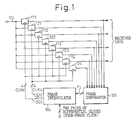
- Figure 1 is a block diagram schematically illustrating one example of a previously-considered receiver circuit, including a clock recovery circuit, wherein the circuit is configured as a 4-way ⁇ 2 type interleaving circuit.
- reference numerals 111 to 114 are data detection units
- 121 to 124 are boundary detection units
- 104 is a phase interpolator
- 105 is a phase comparator.
- reference character DIL is a data input line
- DCL is a data detection clock line
- BCL is a boundary detection clock line
- FL is a feedback line.
- phase interpolator phase adjusting timing signal generating circuit
- CLKd consists of four data detection unit control signals CLKd1, CLKd2, CLKd3, and CLKd4, each with a phase difference of 90 degrees, for example, and these control signals are supplied to the respective data detection units (data detection/discrimination circuits) 111 to 114.
- the clock CLKb consists of four boundary detection unit control signals CLKb1, CLKb2, CLKb3, and CLKb4, each with a phase difference of 90 degrees, for example, and these control signals are supplied to the respective boundary detection units (boundary detection/discrimination circuits) 121 to 124.
- the data detection unit control signals CLKd1, CLKd2, CLKd3, and CLKd4 have a phase difference of 45 degrees relative to the respective boundary detection unit control signals CLKb1, CLKb2, CLKb3, and CLKb4.
- the data detection units 111 to 114 and boundary detection units 121 to 124 perform interleaving by being driven with a 625-MHz clock.
- the data detection units 111 to 114 are each driven, for example, with a 625-MHz clock (data detection unit control signal CLKd1, CLKd2, CLKd3, or CLKd4), detect and discriminate the data carried in the input signal supplied on the data input line DIL, and output the data as received data (reproduced data).
- the outputs of the data detection units 111 to 114 are also supplied to the phase comparator 105.
- boundary detection units 121 to 124 are each driven, for example, with a 625-MHz clock (boundary detection unit control signal CLKb1, CLKb2, CLKb3, or CLKb4), detect and discriminate data boundaries appearing in the input signal supplied on the data input line DIL, and supply the result to the phase comparator 105.
- CLKb1, CLKb2, CLKb3, or CLKb4 boundary detection unit control signal
- the phase comparator 105 compares the outputs of the data detection units 111 to 114 and boundary detection units 121 to 124 based on digital "0s" or "1s", and supplies (feeds back) a feedback signal to the phase interpolator 104 via the feedback line FL.
- Figure 2 is a block diagram showing one configuration example of the phase interpolator in the receiver circuit.
- the phase interpolator 104 comprises mixer circuits 141 and 142, a digital-to-analog converter (DAC) 143, and a frequency divider 144.
- the mixer circuits 141 and 142 each receive a clock signal (four-phase clock) and an output of the DAC 143, synthesize from the four-phase clock a pair of signals differing in phase by 90 degrees, create a phase intermediate between them, generate a clock by applying the phase shift defined by a weight (the output of the DAC 143) to a signal having the intermediate phase, and generate the data detection clock CLKd (CLKd1, CLKd2, CLKd3, CLKd4) and boundary detection clock CLKb (CLKb1, CLKb2, CLKb3, CLKb4) through the frequency divider 144.
- the mixer circuits 141 and 142 each control the phase based on a current value representing the weight; here, the weight for the phase adjustment is created by digitally comparing the phases of the external input clock and internal clock (the data detection clock CLKd and boundary detection clock CLKb) in the phase comparator (105) based on the outputs of the data detection units 111 to 114 and boundary detection units 121 to 124, and is supplied as a phase control signal to the DAC 143.
- the DAC 143 receives a constant current as well as the phase control signal (the output of the phase comparator 105), converts the phase adjusting weight into the current, and supplies the current to the mixer circuits 141 and 142.
- the phases of the clocks CLKd and CLKb are adjusted based on the amount of change of the current.
- clock recovery circuit is used by focusing attention on the fact that the data detection clock is recovered from the input signal
- receiver circuit is used by focusing attention on the fact that the data detection/discrimination circuit, using the recovered clock, detects and discriminates the data carried in the input signal, and outputs the data as the received data.
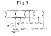
- Figure 3 is a diagram showing an example of latch timing for input signal data and boundaries.
- reference characters t D (n) (t DO (n)), t D (n+1), t D (n+2), and t D (n+3) indicate the ideal timings for the data latched (detected) by the data detection units 111, 112, 113, and 114
- t B (n) (t BO (n)), t B (n+1), t B (n+2), and t B (n+3) indicate the ideal timings for the boundaries latched by the boundary detection units 121, 122, 123, and 124.
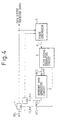
- Figure 4 is a block diagram showing the basic functional configuration of a receiver circuit, including a clock recovery circuit, according to an embodiment of the first mode of the present invention
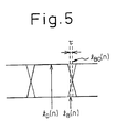
- Figure 5 is a diagram for explaining the operation of the receiver circuit of Figure 4 (including the clock recovery circuit).
- reference numeral 1 is a data detection circuit
- 2 is a boundary detection circuit
- 3 is a boundary skew generating circuit
- 4 is a clock signal generating circuit
- 5 is a phase comparator.
- reference character DIL is a data input line
- DCL is a data detection clock line
- BCL and BCL' are boundary detection clock lines
- FL is a feedback line.
- the clock signal generating circuit 4 generates data detection clock CLKd and boundary detection clock CLKb'.
- the data detection clock CLKd is supplied to the data detection unit 1 via the data detection clock line DCL.
- the boundary detection clock CLKb' is supplied to the boundary skew generating circuit 3 via the boundary detection clock line BCL', and a boundary detection clock CLKb with a prescribed skew provided to it by the boundary skew generating circuit 3 is supplied to the boundary detection unit via the boundary detection clock line BCL.
- the phase comparator 5 compares the outputs of the data detection circuit 1 and boundary detection circuit 2, and supplies (feeds back) a feedback signal to the clock signal generating circuit 4 via the feedback line FL.
- the clock CLKb' output from the clock signal generating circuit 4 is input into the boundary skew generating circuit 3 where the prescribed skew (prescribed time quantity ⁇ ) is applied to it, and the resulting boundary detection clock CLKb is supplied to the boundary detection circuit 2, thereby effectively shifting the boundary detection timing t B (n) by ⁇ forward or backward relative to the original boundary detection timing t BO (n).
- the phase comparator 5 makes decisions to determine a phase lead or phase lag over a number of consecutive bit cells, and the sum is produced as the output of the phase comparator 5.
- a different skew is deliberately given to the decision timing for each decision operation, and the timing position t B (n) is determined which is shifted by the skew ⁇ from the original boundary decision timing t BO (n).
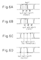
- Figures 6A to 6D are diagrams for explaining the operation of the phase comparator in a receiver circuit (clock recovery circuit) embodying the present invention.
- Figure 6A shows the case [EARLY] where the latch timing t B (n), t D (n) by the internal clock is earlier than the ideal latch timing t BO (n), t DO (n), and Figure 6B shows the case [LATE] where the latch timing t B (n), t D (n) by the internal clock is later than the ideal latch timing t BO (n), t DO (n).
- Figure 6C shows the case [NO TRANSITION] where any transition (from a "0" to a “1” or from a "1" to a “0") does not appear between data (data detection timing t D (n)) and the next data (data detection timing t D (n+1)), where n refers to the bit-cell order.
- Figure 6D shows the case [GLITCH] where, for example, when the same data appears in succession, the boundary detection circuit has latched noise occurring at a boundary position, the data detection circuit has detected a boundary position, or the boundary detection circuit has detected a data position.
- Table 1 The relationship between the data detection timing t D (n) and the boundary detection timing t B (n) is shown in Table 1 below.
- the boundary detection clock CLKb output from the clock signal generating circuit 4 is shifted forward or backward relative to the original boundary detection timing t BO (n); as a result, the input/output characteristic of the phase comparator 5 exhibits a staircase pattern consisting of a number of steps, not a single-step pattern, and this improves the linearity of the phase comparator 5 and serves to stabilize the feedback circuit operation for clock recovery.
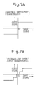
- Figures 7A and 7B are diagrams for explaining one example of the operation of a receiver circuit embodying the present invention: Figure 7A shows a nonlinear input/output characteristic, and Figure 7B shows a staircase-like input/output characteristic.
- the circuit of Figure 4 which shows the basic functional configuration of the invention differs from the previously-considered clock recovery circuit by the inclusion of the boundary skew generating circuit 3 with provisions made to shift the boundary detection timing forward or backward relative to the original timing.
- the phase comparator 5 makes decisions to determine a phase lead or phase lag over a number of consecutive bit cells, and the sum is produced as the output of the phase comparator 5.
- a different skew is deliberately given to the decision timing for each decision operation.
- the input/output characteristic of the phase comparator exhibits a staircase pattern consisting of four steps as shown in Figure 7B.
- This characteristic can be interpreted as having an improved linearity compared with the previously-considered nonlinear input/output characteristic consisting of a single step (see Figure 7A).
- a characteristic substantially linear over the time duration 4 ⁇ can be obtained. Therefore, if the value of 4 ⁇ is set approximately equal to the maximum value of the jitter input to the system, the phase comparator 5 can always be operated within a linear range. As a specific example, if the value of 4 ⁇ is set approximately equal to 0.5 UI (Unit Interval: Data clock period, for example, the clock period of a 2.5 GHz external clock), that would suffice for practical purposes.
- 0.5 UI Unit Interval: Data clock period, for example, the clock period of a 2.5 GHz external clock
- phase comparator of an embodiment of the present invention has an input/output characteristic of improved linearity compared with the previously-considered clock recovery circuit (receiver circuit) having a single-step nonlinear characteristic, the predictability of the characteristics of the clock recovery circuit can be improved by reducing not only the amplitude of the limit cycle signal inherent in a nonlinear system but also the jitter dependence and signal level dependence of the feedback loop characteristic.
- FIG 8 is a block diagram schematically showing a first embodiment of a receiver circuit according to the present invention, wherein the circuit is configured as a 4-way ⁇ 2 type interleaving circuit.
- reference numerals 11 to 14 are data detection units
- 21 to 24 are boundary detection units
- 31 to 34 are boundary skew generating units (buffer delay circuits)
- 4 is a clock signal generating circuit
- 5 is a phase comparator.
- DIL is a data input line
- DCL is a data detection clock line
- BCL is a boundary detection clock line
- FL is a feedback line.
- the receiver circuit (clock recovery circuit) of the first embodiment comprises four data detection units 11 to 14 and four boundary detection units 21 to 24, and the data detection units 11 to 14 and boundary detection units 21 to 24 perform interleaving.
- the clock CLKd consists of four data detection unit control signals CLKd1, CLKd2, CLKd3, and CLKd4, each with a phase difference of 90 degrees, for example, and these control signals are supplied to the four data detection units (data detection/discrimination circuits) 11 to 14, respectively.
- the clock CLKb consists of four boundary detection unit control signals CLKb1, CLKb2, CLKb3, and CLKb4, each with a phase difference of 90 degrees, for example, and these control signals are supplied to the four boundary detection units (boundary detection/discrimination circuits) 21 to 24, respectively.
- the data detection unit control signals CLKd1, CLKd2, CLKd3, and CLKd4 have a phase difference of 45 degrees relative to the respective boundary detection unit control signals CLKb1, CLKb2, CLKb3, and CLKb4.
- the data detection units 11 to 14 and boundary detection units 21 to 24 perform interleaving by being driven with a 625-MHz clock.
- the data detection units 11 to 14 are each driven, for example, with a 625-MHz clock (data detection unit control signal CLKd1, CLKd2, CLKd3, or CLKd4), detect and discriminate the data carried in the input signal supplied on the data input line DIL, and output the data as received data (reproduced data).
- the outputs of the data detection units 11 to 14 are also supplied to the phase comparator 5.
- boundary detection units 21 to 24 are each driven, for example, with a 625-MHz clock (boundary detection unit control signal CLKb1, CLKb2, CLKb3, or CLKb4), detect and discriminate data boundaries appearing in the input signal supplied on the data input line DIL, and supply the result to the phase comparator 5.
- CLKb1, CLKb2, CLKb3, or CLKb4 boundary detection unit control signal
- the phase comparator 5 compares the outputs of the data detection units 11 to 14 and boundary detection units 21 to 24, and supplies (feeds back) a feedback signal to the clock signal generating circuit 4 via the feedback line FL.
- Figure 9 is a diagram for explaining the operation of the receiver circuit of Figure 8.
- the boundary skew generating units 31, 32, 33, and 34 provide skews of -3/2 ⁇ , -1/2 ⁇ , 1/2 ⁇ , and 3/2 ⁇ in this order to the boundary latch timings of the boundary detection units 21, 22, 23, and 24, where ⁇ is a predefined time quantity, thereby shifting the boundary latch timings by the respective values relative to their original timings (ideal timings).
- Figure 10 is a diagram showing, by way of example, the results of simulations for the phase stability performance of the receiver circuit, the simulations being based on clock recovery circuit models, one according to an embodiment of the present invention and the other according to the previously-considered model for comparison; more specifically, the phase stability performance was simulated by creating models using the C language.
- Figure 10 data of a pattern "1, 0, 1, 0, " was input, and the amplitude due to the bang-bang control in each clock recovery circuit model was observed.
- reference character L0 (dashed line) shows the simulation result for the previously-considered receiver circuit
- L1 (solid line) indicates the simulation result for the receiver circuit embodying the present invention.
- phase deviation (fluctuation in timing) is plotted along the vertical axis, and the time along the horizontal axis.
- FIG 11 is a block diagram schematically showing a second embodiment of a receiver circuit according to the present invention.
- the circuit block configuration of the second embodiment shown in Figure 11 is fundamentally the same as that shown in Figure 1, but the difference lies in the configuration of the phase interpolator 40. That is, in the second embodiment, the phase interpolator 40 includes the function of varying the boundary detection timing in the boundary detection units 21 to 24.
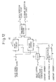
- Figure 12 is a block diagram showing one configuration example of the phase interpolator in the receiver circuit of Figure 11.
- the phase interpolator 40 comprises mixer circuits 46 and 47, a digital-to-analog converter (DAC) 43, a frequency divider 44, and a modulating DAC 45.
- the mixer circuit 46 receives a clock signal (four-phase clock) and an output of the DAC 43, synthesizes, from the four-phase clock, a pair of signals differing in phase by 90 degrees, creates a phase intermediate between them, and generates a clock by applying the phase shift defined by a weight (the output of the DAC 43) to a signal having the intermediate phase.
- the mixer circuit 47 receives the clock signal, an output of the DAC 43, and an output of the modulating DAC 45, synthesizes from the four-phase clock a pair of signals differing in phase by 90 degrees, creates a phase intermediate between them, and generates a clock by applying the phase shift defined by a weight (the output of the DAC 43 and the output of the modulating DAC 45) to a signal having the intermediate phase.
- the outputs of the mixer circuits 46 and 47 are supplied to the frequency divider 44, which generates the data detection clock CLKd (CLKd1, CLKd2, CLKd3, and CLKd4) and boundary detection clock CLKb (CLKb1, CLKb2, CLKb3, and CLKb4).
- the mixer circuits 46 and 47 each control the phase based on a current value representing the weight; here, the weight for the phase adjustment is created by digitally comparing the phases of the external input clock and internal clock (the data detection clock CLKd and boundary detection clock CLKb) in the phase comparator (5) based on the outputs of the data detection units 11 to 14 and boundary detection units 21 to 24, and is supplied as a phase control signal to the DAC 43.
- the weight for the phase adjustment is created by digitally comparing the phases of the external input clock and internal clock (the data detection clock CLKd and boundary detection clock CLKb) in the phase comparator (5) based on the outputs of the data detection units 11 to 14 and boundary detection units 21 to 24, and is supplied as a phase control signal to the DAC 43.
- the DAC 43 receives a constant current as well as the phase control signal (the output of the phase comparator 5), converts the phase adjusting weight into the current, and supplies the current to the mixer circuits 46 and 47.
- the phases of the clocks CLKd and CLKb are adjusted in the mixer circuit 46 based on the amount of change of the current supplied from the DAC 43 and, in the mixer circuit 47, based on the amount of change of the current supplied from the modulating DAC 45 as well as that supplied from the DAC 43.
- a digitally expressed external modulating code is applied to the modulating DAC 45 for conversion into a current, and the output current of the modulating DAC 45 is supplied to the mixer circuit 47, thereby providing a skew to the boundary clock signal (boundary detection clock).
- the modulating code supplied to the modulating DAC 45 is digitally expressed, a programmable skew can be generated and, with this skew, the boundary detection timing can be effectively shifted forward or backward relative to the original boundary position.
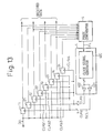
- Figure 13 is a block diagram schematically showing a third embodiment of a receiver circuit according to the present invention
- Figure 14 is a block diagram showing one configuration example of a boundary detection/discrimination clock buffer (boundary detection clock buffer) in the receiver circuit of Figure 13.
- the clock signal generating circuit 4 in the receiver circuit (clock recovery circuit) of the third embodiment comprises a clock signal generator 400 and clock buffers 401 and 402.
- Data detection clocks CLKd (CLKd1 to CLKd4) are supplied to the respective data detection units 11 to 14 via the data detection clock buffer 401, while boundary detection clocks CLKb (CLKb1 to CLKb4) are supplied to the respective boundary detection units 21 to 24 via the boundary detection clock buffer 402.
- the boundary detection clock buffer 402 receives the four-phase clock from the clock signal generator 400, and generates the boundary detection clocks CLKb (CLKb1 to CLKb4) via two-stage inverters 421/431 to 424/434.
- the first-stage inverters 421 to 424 p-channel MOS transistors 421p to 424p and n-channel MOS transistors 421n to 424n are respectively chosen to have different gate widths W.
- skews of -3/2 ⁇ , -1/2 ⁇ , 1/2 ⁇ , and 3/2 ⁇ are given to the boundary detection clocks CLKb1, CLKb2, CLKb3, and CLKb4, thereby shifting the respective boundary latch timings from their original timing positions.
- reference character VD designates a power supply
- GND is ground
- cp and cn are fixed values.
- the boundary detection clocks CLKb1, CLKb2, CLKb3, and CLKb4 provided with different skews as described above are supplied to the respective boundary detection units 21, 22, 23, and 24.
- prescribed skews are given to the boundary detection clocks CLKb1 to CLKb4 by controlling the transistor sizes of the first-stage inverters in the boundary detection clock buffer 402 that outputs the clocks supplied to the boundary detection/discrimination circuit 2 (boundary detection units 21 to 24);
- the first-stage inverters 421 to 424 may be constructed from transistors of the same size, and capacitors 441 to 444 with capacitance increasing in the order of 441, 442, 443, and 444 may be provided on the output sides of the respective inverters 421 to 424 so that different skews can be given to the respective boundary detection clocks CLKb1 to CLKb4.
- the transistor sizes of the second-stage inverters 431 to 434 may be adjusted.
- Figure 15 is a block diagram schematically showing a fourth embodiment of a receiver circuit according to the present invention.
- the boundary skew generating circuit 3 is constructed from a variable delay line (VDL) circuit. That is, in the fourth embodiment, the boundary detection clock CLKb output from the clock signal generating circuit 4 is supplied to the boundary detection circuit 2 via the VDL circuit 3.
- VDL variable delay line
- the VDL circuit 3 is constructed, for example, from a plurality of delay lines 301 to 304 selectively controlled by an external control signal CS, and each of the delay lines 301 to 304 comprises, for example, a buffer, a switch, etc.
- a suitable skew is given to the boundary detection clock CLKb by controlling the ON/OFF operation of each switch by the external control signal.
- the boundary detection timing is effectively shifted forward or backward relative to the original boundary position; it will, however, be noted that the specific configuration for achieving this is not limited to any one of the above embodiments, but various other configurations are also possible.
- the linearity of the phase comparator is improved as described above, the amplitude of the limit cycle signal can be reduced, and the predictability of the circuit characteristics can be improved by reducing the jitter dependence and signal level dependence of the feedback loop characteristic.
- a clock recovery circuit and receiver circuit that achieves high-speed signal transmission by reducing the amplitude of the limit cycle signal and also reducing the jitter dependence and signal level dependence of the feedback loop characteristic (to facilitate prediction of the circuit characteristics).
- Figure 16 is a block diagram schematically illustrating one example of a previously-considered receiver circuit, including the clock recovery circuit.
- reference numeral 101 is a data detection/discrimination circuit
- 102 is a changing point detection/discrimination circuit
- 104 is a phase adjusting timing signal generating circuit (phase interpolator)
- 105 is a phase comparator circuit.
- DIL is a data input line
- DOL is a data output line
- DCL is a data detection clock line
- BCL is a changing point detection clock line
- FL is a feedback line.
- a clock is supplied to the phase adjusting timing signal generating circuit 104 which integrates and compares the weighted sum of the input clocks and thereby generates clocks (CLKd and CLKb) of the phases corresponding to the weight value, and supplies the data detection clock CLKd to the data detection/discrimination circuit 101 and the changing point detection clock CLKb to the changing point detection/discrimination circuit 102.
- the phase comparator circuit 105 compares the outputs of the data detection/discrimination circuit 101 and changing point detection/discrimination circuit 102, and feeds back the feedback signal (control signal) to the phase adjusting timing signal generating circuit 104 via the feedback line FL.
- clock recovery circuit is used by focusing attention on the fact that the data detection clock is recovered from the input signal
- receiver circuit is used by focusing attention on the fact that the data detection/discrimination circuit, using the recovered clock, detects and discriminates the data carried in the input signal, and outputs the data as the received data.
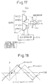
- Figure 17 is a block circuit diagram showing one example of the phase adjusting timing signal generating circuit 104 in the receiver circuit of Figure 16, and Figure 18 is a waveform diagram for explaining the operation of the phase adjusting timing signal generating circuit of Figure 17.
- reference numerals 104a and 104b are mixer circuits (phase mixers), 104c is a comparator, and 104d is a digital-to-analog converter (D/A converter).
- the mixer circuits 104a and 104b each receive clocks ⁇ 0 and ⁇ 0b or ⁇ 1 and ⁇ 1b and an output of the D/A converter 104d, apply a weight (the output of the D/A converter 104d) to each clock, and thereby output a clock ⁇ ( ⁇ b) having a phase intermediate between the respective clocks through the comparator 104c.
- the weight is given by the control signal output from the phase comparator circuit 105.
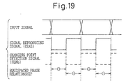
- Figure 19 is a diagram showing the timing relationship between the signals in the receiver circuit of Figure 16.
- the phase adjusting timing signal generating circuit 104 described above generates a signal reproducing signal (data detection clock CLKd) and a changing point detection signal (changing point detection clock CLKb), each as a clock having a pulse width one half the pulse width of one bit of the input signal, and supplies them to the data detection/discrimination circuit 101 and the changing point detection/discrimination circuit 102, respectively.
- the phase relationship between the data detection clock CLKd and the changing point detection clock CLKb is such that their rising edges are equally spaced apart from each other, that is, when the rise timing of the changing point detection clock CLKb is at the changing point, the rise timing of the data detection clock CLKd is located at the phase center of the input signal (data eye).
- Figure 20 is a block diagram schematically illustrating another example of a previously-considered receiver circuit, including the clock recovery circuit, wherein the circuit is configured as a 4-way ⁇ 2 type interleaving circuit.
- reference numerals 111 to 114 are data detection units
- 121 to 124 are changing point detection units
- 103 is a frequency divider
- 104 is a phase adjusting timing signal generating circuit
- 105 is a phase comparator circuit.
- two pairs of differential clock signals ( ⁇ 0, ⁇ 0x; ⁇ 1, ⁇ 1x) are supplied as a four-phase input signal (four-phase clock) to the phase adjusting timing signal generating circuit 104 which integrates and compares the weighted sum of the input signals and generates, through the frequency divider 103, clocks (CLKd and CLKb) of the phases corresponding to the weight value.
- the clock CLKd consists of four data detection unit control signals CLKd1, CLKd2, CLKd3, and CLKd4, each with a phase difference of 90 degrees, for example, and these control signals are supplied to the respective data detection units (data detection/discrimination circuits) 111 to 114.
- the clock CLKb consists of four changing point detection unit control signals CLKb1, CLKb2, CLKb3, and CLKb4, each with a phase difference of 90 degrees, for example, and these control signals are supplied to the respective changing point detection units (changing point detection/discrimination circuits) 121 to 124.
- the data detection unit control signals CLKd1, CLKd2, CLKd3, and CLKd4 have a phase difference of 45 degrees relative to the respective changing point detection unit control signals CLKb1 CLKb2, CLKb3, and CLKb4.
- the data detection units 111 to 114 and changing point detection units 121 to 124 perform interleaving by being driven with a 625-MHz clock.
- the data detection units 111 to 114 are each driven, for example, with a 625-MHz clock (data detection unit control signal CLKd1, CLKd2, CLKd3, or CLKd4), detect and discriminate the data carried in the input signal supplied on the data input line DIL, and output the data as received data (reproduced signal).
- the outputs of the data detection units 111 to 114 are also supplied to the phase comparator circuit 105.
- the changing point detection units 121 to 124 are each driven, for example, with a 625-MHz clock (changing point detection unit control signal CLKb1, CLKb2, CLKb3, or CLKb4), detect and discriminate changing points appearing in the input signal supplied on the data input line DIL, and supply the result to the phase comparator circuit 105.
- a 625-MHz clock changing point detection unit control signal CLKb1, CLKb2, CLKb3, or CLKb4
- the phase comparator circuit 105 compares the outputs of the data detection units 111 to 114 and changing point detection units 121 to 124, and supplies (feeds back) a feedback signal to the phase adjusting timing signal generating circuit 104 via the feedback line FL.
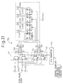
- Figure 21 is a block circuit diagram showing one example of the phase adjusting timing signal generating circuit in the receiver circuit of Figure 20, and Figure 22 is a diagram showing signal timings in the phase adjusting timing signal generating circuit of Figure 21.
- the phase adjusting timing signal generating circuit 104 comprises mixer circuits (phase mixers) 141 and 142, a digital-to-analog converter (D/A converter) 143, and comparators 146 and 147.
- the mixer circuits 141 and 142 each receive clock signals (four-phase clock) ⁇ 0, ⁇ 0x; ⁇ 1, ⁇ 1x and an output of the D/A converter 143, apply a weight (the output of the D/A converter 143) to each clock signal and thereby generate clocks ⁇ a, ⁇ ax; ⁇ b, ⁇ bx each having a phase intermediate between the respective clocks, and generate, through the frequency divider 103, data detection clocks CLKd (CLKd1, CLKd2, CLKd3, CLKd4) and changing point detection clocks CLKb (CLKb1, CLKb2, CLKb3, CLKb4).
- the mixer circuits 141 and 142 each control the phase based on a current value representing the weight; here, the weight for the phase adjustment is created by the phase comparator circuit (105) digitally comparing the phases of the clocks obtained from the outputs of the data detection units 111 to 114 and changing point detection units 121 to 124, and is supplied as a phase control signal to the D/A converter 143.
- the D/A converter 143 receives a constant current as well as the phase control signal (the output of the phase comparator circuit 105), converts the phase adjusting weight into the current, and supplies the current to the mixer circuits 141 and 142.
- the phases of the clocks CLKd and CLKb are adjusted based on the amount of change of the current.
- Figure 23 is a diagram showing signal timings in the previously-considered receiver circuit and, more specifically, the input signal and the phase relationship between the data detection clock CLKd supplied to the data detection/discrimination circuit 101 and the changing point detection clock CLKb supplied to the changing point detection/discrimination circuit 102 in Figure 16 or the phase relationship between the data detection unit control signals CLKd1 to CLKd4 supplied to the data detection units 111 to 114 and the changing point detection unit control signals CLKb1 to CLKb4 supplied to the changing point detection units 121 to 124 in Figure 20; as shown here, the phases of the respective clocks or signals are equally spaced apart from each other.
- the data detection clock CLKd (CLKd1 to CLKd4) and the changing point detection clock CLKb (CLKb1 to CLKb4) have a equispaced phase relationship relative to each other with a phase difference equivalent to one half of one bit of input signal transmission rate. Accordingly, when the changing point detection clock CLKb is at the changing point of the input signal, the data detection clock CLKd is located at the phase center of the input signal.
- reference character CLKd-01 indicates one rise timing of a particular data detection clock CLKd (for example, the data detection unit control signal CLKd1) supplied to the data detection/discrimination circuit 101 (the data detection unit 111), and CLKd-02 indicates the next rise timing immediately subsequent to the rise timing CLKd-01 of that particular data detection clock CLKd (the data detection unit control signal CLKd1).
- reference character CLKb-01 indicates the rise timing of the changing point detection clock CLKb (the changing point detection unit control signal CLKb1) supplied to the changing point detection/discrimination circuit 102 (the changing point detection unit 121), the rise timing occurring between the rise timings CLKd-01 and CLKd-02 of the data detection clock CLKd (the data detection unit control signal CLKd1).
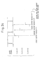
- Figures 24 and 25 are diagrams for explaining the timing of the changing point detection signal relative to the input signal in the receiver circuit, and more specifically, the relationships of the rise timings CLKd-01 and CLKd-02 of the data detection clock CLKd and the rise timing CLKb-01 of the changing point detection clock CLKb relative to the input signal.
- the illustrated example shows the case where the input signal alternates between a "1" and a "0".
- the phase comparator circuit 105 can determine whether the phase of the timing signal is advanced or delayed with respect to the input signal by referring to the first to third output results, and feeds back the resulting control signal to the phase adjusting timing signal generating circuit 104 via the feedback line FL to adjust the phase of the timing signal with respect to the input signal.
- the phase comparator circuit 105 feeds back a control signal for delaying the phase of the timing signal (the output signal of the phase adjusting timing signal generating circuit 104) to the phase adjusting timing signal generating circuit 104; conversely, when it is determined that the phase of the timing signal is delayed with respect to the input signal, a control signal for advancing the phase of the timing signal is fed back to the phase adjusting timing signal generating circuit 104.
- the timing of the changing point detection clock CLKb (changing point detection unit control signals CLKb1 to CLKb4) is made to synchronize in phase to the change point of the input signal.
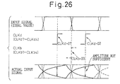
- Figure 26 is a diagram for explaining the problem of the previously-considered receiver circuit by adding an actual input signal waveform to the waveform diagram of Figure 23.
- the data detection/discrimination circuit 101 detects and discriminates the signal at a position where a sufficient amplitude cannot be obtained, and this has lead to the problem of signal reproduction error.
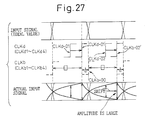
- Figure 27 is a diagram for explaining the operation another receiver circuit embodying the present invention (second mode).
- the timing of the data detection clock CLKd is shifted from the phase center of the input signal (the center of the data eye); for example, when the maximum amplitude position of the input signal is displaced from the center of the data eye in the lagging direction because of the limited frequency band of the signal transmission line, the timing of the data detection clock CLKd is shifted in the lagging direction so that after the feedback loop is stabilized, data can be detected at a position where a sufficient amplitude can be obtained.
- signal reproduction accuracy is enhanced by shifting (adjusting) the timing of the data detection clock CLKd from the phase center of the input signal (the center of the data eye) to the phase (position) where a sufficient and effective signal amplitude can be obtained.
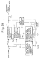
- FIG 28 is a block diagram showing a fifth embodiment of a receiver circuit (clock recovery circuit) according to the present invention.
- reference numeral 1 is a data detection/discrimination circuit
- 2 is a changing point detection/discrimination circuit
- 41 is a data detection phase adjusting timing signal generating circuit (data detection phase interpolator)
- 42 is a changing point detection phase adjusting timing signal generating circuit (changing point detection phase interpolator)
- 5 is a phase comparator circuit.
- DIL is a data input Line
- DOL is a data output line
- DCL is a data detection clock line
- BCL is a changing point detection clock line
- FL1 and FL2 are feedback lines.
- the data detection phase adjusting timing signal generating circuit 41 and the changing point detection phase adjusting timing signal generating circuit 42 together constitute a clock signal generating circuit (phase adjusting timing signal generating means).
- the receiver circuit (clock recovery circuit) of the fifth embodiment differs from the previously-considered circuit in that the phase adjusting timing signal generating circuit 104 in Figure 16 is divided into the data detection phase adjusting timing signal generating circuit 41 and the changing point detection phase adjusting timing signal generating circuit 42, and in that the phase comparator circuit 5 supplies control signals CS1 and CS2 separately to the respective circuits via the respective feedback lines FL1 and FL2.
- the control signal CS1 supplied to the data detection phase adjusting timing signal generating circuit 41 and the control signal CS2 supplied to the changing point detection phase adjusting timing signal generating circuit 42 are controlled separately from each other.
- the changing point detection phase adjusting timing signal generating circuit 42 is feedback-controlled by the control signal CS2 supplied from the phase comparator circuit 5 via the feedback clock line FL2 in such a manner that the changing point detection clock CLKb output from it is phase synchronized to the change point of the input signal, as in the case of the circuit shown in Figure 16.
- the data detection phase adjusting timing signal generating circuit 41 is feedback-controlled by the control signal CS1 supplied from the phase comparator circuit 5 via the feedback clock line FL1 in such a manner that the data detection clock CLKd' output from it occurs at optimum timing appropriate to the actual input signal waveform (for example, at a position delayed from the center of the data eye when the maximum amplitude position of the input signal is delayed with respect to the center of the data eye).
- clock recovery circuit The basic configuration of the receiver circuit (clock recovery circuit) is the same as that of the previously-considered circuit shown in Figure 16; that is, clocks (for example, four-phase clocks ⁇ 0, ⁇ 0b; ⁇ 1, ⁇ 1b) are supplied to the data detection phase adjusting timing signal generating circuit 41 and the changing point detection phase adjusting timing signal generating circuit 42, the weighted sum of the input clocks is integrated and compared to generate clocks (CLKd' and CLKb) of the phases corresponding to the weight value, and the data detection clock CLKd' is supplied to the data detection/discrimination circuit 1 and the changing point detection clock CLKb to the changing point detection/discrimination circuit 2.
- clocks for example, four-phase clocks ⁇ 0, ⁇ 0b; ⁇ 1, ⁇ 1b
- the phase comparator circuit 5 compares the outputs of the data detection/discrimination circuit 1 and changing point detection/discrimination circuit 2, and feeds back the feedback signals (control signals) to the data detection phase adjusting timing signal generating circuit 41 and the changing point detection phase adjusting timing signal generating circuit 42 via the feedback lines FL1 and FL2, respectively.
- the changing point detection clock CLKb and the data detection clock CLKd' can be made to have a phase relationship other than an equispaced phase relationship, and even when the input signal has a frequency band constraint, for example, the signal can be reproduced at the phase (position) where the amplitude of the input signal is large.
- the changing point detection clock CLKb and the data detection clock CLKd' can be made to have an equispaced phase relationship, as in the previously-considered circuitry, by supplying the same control signal to the data detection phase adjusting timing signal generating circuit 41 and the changing point detection phase adjusting timing signal generating circuit 42.
- Figure 29 is a block diagram showing a sixth embodiment of a receiver circuit according to the present invention
- Figure 30 is a diagram showing one example of an offset adding circuit in the receiver circuit of Figure 29.
- control signal CS (CS2) from the phase comparator 50 is not only supplied directly to the changing point detection phase adjusting timing signal generating circuit 42, but also supplied as the control signal CS1 to the data detection phase adjusting timing signal generating circuit 41 via the offset adding circuit (offset adjusting circuit) 6.
- the feedback loop consisting of the changing point detection/discrimination circuit 2, phase comparator circuit 50, and changing point detection phase adjusting timing signal generating circuit 42 operates in such a manner that the changing point detection signal is phase synchronized to the changing point of the input signal.
- the offset adding circuit 6 produces an output "000010". That is, the 6-bit code "000001” is supplied as the control signal CS2 to the changing point detection phase adjusting timing signal generating circuit 42, while the 6-bit code "000010” with one bit added to the 6-bit code of the control signal CS2 is supplied as the control signal CS1 to the data detection phase adjusting timing signal generating circuit 41.
- the data detection/discrimination circuit 1 detects data by using the data detection clock CLKd' whose phase is delayed compared with the data detection clock CLKd in the previously-considered receiver circuit (see, for example, Figure 23).
- the offset add value OAV applied to the offset adding circuit 6 is chosen to give the optimum offset according to the position where the signal amplitude is maximum by considering, for example, the characteristic of the signal transmission path, etc.
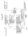
- Figure 31 is a block diagram showing a seventh embodiment of a receiver circuit according to the present invention
- Figure 32 is a diagram showing one example of an offset subtracting circuit in the receiver circuit of Figure 31.
- the offset adding circuit 6 provided on the input side of the data detection phase adjusting timing signal generating circuit 41 in the sixth embodiment is replaced by the offset subtracting circuit (offset adjusting circuit) 60 which, in the seventh embodiment, is provided on the input side of the changing point detection phase adjusting timing signal generating circuit 42.
- control signal CS (CS1) from the phase comparator 50 is not only supplied directly to the data detection phase adjusting timing signal generating circuit 41, but also supplied as the control signal CS2 to the changing point detection phase adjusting timing signal generating circuit 42 via the offset subtracting circuit 60.
- the feedback loop consisting of the changing point detection/discrimination circuit 2, phase comparator circuit 50, offset subtracting circuit 60, and changing point detection phase adjusting timing signal generating circuit 42 operates in such a manner that the changing point detection signal is phase synchronized to the changing point of the input signal.
- the offset subtracting circuit 60 produces an output "000000". That is, the 6-bit code "000001” is supplied as the control signal CS1 to the data detection phase adjusting timing signal generating circuit 41, while the 6-bit code "000000” with one bit subtracted from the 6-bit code of the control signal CS1 is supplied as the control signal CS2 to the changing point detection phase adjusting timing signal generating circuit 42.
- the data detection/discrimination circuit 1 detects data by using the data detection clock CLKd' whose phase is delayed compared with the data detection clock CLKd in the previously-considered receiver circuit.
- the offset subtract value OSV applied to the offset subtracting circuit 60 is, of course, chosen to give the optimum offset according to the position where the signal amplitude is maximum by considering, for example, the characteristic of the signal transmission path, etc.
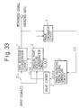
- Figure 33 is a block diagram showing an eighth embodiment of a receiver circuit according to the present invention
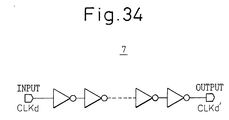
- Figure 34 is a diagram showing one example of a delay circuit in the receiver circuit of Figure 33.
- the eighth embodiment differs from the previously-considered circuitry shown in Figure 16 in that the data detection clock CLKd, which was supplied directly to the data detection/discrimination circuit 101 in Figure 16, is delayed through the delay circuit 7 and supplied as a data detection clock CLKd' to the data detection/discrimination circuit 1.
- the delay circuit 7 is constructed, for example, by connecting a plurality (even number) of inverters in series.
- the number of inverter stages that determines the amount of delay introduced by the delay circuit 7 is determined, for example, according to the position where the signal amplitude is maximum by considering the characteristic of the signal transmission path, etc.
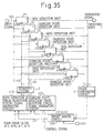
- Figure 35 is a block diagram showing a ninth embodiment of a receiver circuit according to the present invention, wherein the circuit is configured as a 4-way ⁇ 2 type interleaving circuit.
- reference numerals 11 to 14 are data detection units
- 21 to 24 are changing point detection units
- 3 is a frequency divider
- 410 is a data detection phase adjusting timing signal generating circuit
- 420 is a changing point detection phase adjusting timing signal generating circuit
- 5 is a phase comparator circuit
- 600 is an offset adding circuit.
- the ninth embodiment shown in Figure 35 corresponds to the sixth embodiment previously shown in Figures 29 and 30, and is one where an embodiment of the present invention is applied to the previously-considered circuitry shown in Figures 20 and 21. That is, in the receiver circuit of the ninth embodiment, two pairs of differential clock signals ( ⁇ 0, ⁇ 0x; ⁇ 1, ⁇ 1x) are supplied as a four-phase input signal (four-phase clock) to the data detection phase adjusting timing signal generating circuit 410 and the changing point detection phase adjusting timing signal generating circuit 420, which integrate and compare the weighted sum of the input signals and generate, through the frequency divider 3, clocks (CLKd' and CLKb) of the phases corresponding to the weight value.
- the clock CLKd' consists of four data detection unit control signals CLKd1', CLKd2', CLKd3', and CLKd4', each with a phase difference of 90 degrees, for example, and these control signals are supplied to the respective data detection units (data detection/discrimination circuits) 11 to 14.
- the clock CLKb is the same as that in the previously-considered circuitry and consists of four changing point detection unit control signals CLKb1, CLKb2, CLKb3, and CLKb4, each with a phase difference of 90 degrees, for example, and these control signals are supplied to the respective changing point detection units (changing point detection/discrimination circuits) 21 to 24.
- the data detection units 11 to 14 and changing point detection units 21 to 24 perform interleaving by being driven with a 625-MHz clock.
- the data detection units 11 to 14 are each driven, for example, with a 625-MHz clock (data detection unit control signal CLKd1, CLKd2, CLKd3, or CLKd4), detect and discriminate the data carried in the input signal supplied on the data input line DIL, and output the data as received data (reproduced signal).
- the outputs of the data detection units 11 to 14 are also supplied to the phase comparator circuit 5.
- the changing point detection units 21 to 24 are each driven, for example, with a 625-MHz clock (changing point detection unit control signal CLKb1, CLKb2, CLKb3, or CLKb4), detect and discriminate data changing points appearing in the input signal supplied on the data input line DIL, and supply the result to the phase comparator circuit 5.
- CLKb1, CLKb2, CLKb3, or CLKb4 changing point detection unit control signal
- the phase comparator circuit 5 compares the outputs of the data detection units 11 to 14 and changing point detection units 21 to 24, and outputs the- control signal CS (CS2).
- the control signal CS from the phase comparator circuit 5 is not only supplied as the control signal CS2 to the changing point detection phase adjusting timing signal generating circuit 420, but also supplied as the control signal CS1 to the data detection phase adjusting timing signal generating circuit 410 via the offset adding circuit 600.
- the configuration of the offset adding circuit 600 is the same as that in the previously described sixth embodiment (see Figure 30).
- an offset subtracting circuit may be provided on the input side of the changing point detection phase adjusting timing signal generating circuit 420.
- Figure 36 is a block circuit diagram showing one example of the phase adjusting timing signal generating block in the receiver circuit of Figure 35.
- the phase adjusting timing signal generating block comprises the data detection phase adjusting timing signal generating circuit 410, changing point detection phase adjusting timing signal generating circuit 420, and frequency divider 3.
- the data detection phase adjusting timing signal generating circuit 410 comprises a mixer circuit (phase mixer) 411, a comparator 412, and a D/A converter 413;
- the changing point detection phase adjusting timing signal generating circuit 420 comprises a mixer circuit 421, a comparator 422, and a D/A converter 423.
- the mixer circuit 411 receives clock signals (four-phase clock) ⁇ 0, ⁇ 0x; ⁇ 1, ⁇ 1x and an output of the D/A converter 413, and applies a weight (the output of the D/A converter 413) to each clock signal and thereby generates clocks ⁇ a and ⁇ ax each having a phase intermediate between the respective clocks; likewise, the mixer circuit 421 receives the clock signals (four-phase clock) ⁇ 0, ⁇ 0x; ⁇ 1, ⁇ 1x and an output of the D/A converter 423, and applies a weight to each clock signal and thereby generates clocks ⁇ b and ⁇ bx each having a phase intermediate between the respective clocks.
- clocks ⁇ a, ⁇ ax and ⁇ b, ⁇ bx are supplied to the frequency divider 3, which outputs the data detection clock CLKd' (CLKd1', CLKd2', CLKd3', CLKd4') and changing point detection clock CLKb (CLKb1, CLKb2, CLKb3, CLKb4).
- the D/A converter 423 receives directly the output (control signal CS (CS2)) of the phase comparator circuit 5, converts the phase adjusting weight into current, and supplies the current to the mixer circuit 421.
- the D/A converter 413 receives the control signal CS1, created by the offset adding circuit 600 by adding the offset adding value OAV to the output (control signal CS) of the phase comparator 5, converts the phase adjusting weight into current, and supplies the current to the mixer circuit 411.
- signal reproduction accuracy is enhanced by shifting (adjusting) the timing of the data detection clock from the phase center of the input signal to the phase position where a sufficient and effective signal amplitude can be obtained.
- the input signal reproduction timing can be taken at the position where the amplitude of the input signal can be sufficiently secured, and the error rate of signal reproduction can thus be improved.
Landscapes
- Engineering & Computer Science (AREA)
- Computer Networks & Wireless Communication (AREA)
- Signal Processing (AREA)
- Synchronisation In Digital Transmission Systems (AREA)
Abstract
Description

Claims (59)
- A clock recovery circuit which includes a boundary detection/discrimination circuit for detecting or discriminating a boundary in an input signal in accordance with a first signal, and which performs clock recovery by controlling the timing of said first signal in accordance with said detected boundary, wherein
boundary detection timing in said boundary detection/discrimination circuit is varied by controlling said first signal. - The clock recovery circuit as claimed in claim 1, wherein said boundary detection/discrimination circuit detects said boundary in said input signal at a timing variably displaced from the timing at which said boundary should otherwise be detected.
- The clock recovery circuit as claimed in claim 1, wherein said boundary detection/discrimination circuit detects said boundary in said input signal at a predetermined timing.
- The clock recovery circuit as claimed in claim 1, wherein said boundary detection/discrimination circuit detects said boundary in said input signal at a dynamically controlled timing.
- The clock recovery circuit as claimed in any preceding claim, further comprising a phase interpolator for delaying said first signal by different times, and wherein modulation is applied on a code supplied to said phase interpolator.
- The clock recovery circuit as claimed in claim 5, further comprising a digital-to-analog converter for applying modulation on said code supplied to said phase interpolator, and wherein weighted modulation is applied by said digital-to-analog converter.
- The clock recovery circuit as claimed in any preceding claim, further comprising a variable delay circuit for delaying said first signal by different times.
- The clock recovery circuit as claimed in any preceding claim, wherein said boundary detection/discrimination circuit includes a plurality of boundary detection units, and wherein each of said boundary detection units detects a boundary in accordance with a boundary detection unit control signal.
- The clock recovery circuit as claimed in claim 8, wherein said each boundary detection unit detects said boundary in said input signal at a timing variably displaced from the timing at which said boundary should otherwise be detected.
- The clock recovery circuit as claimed in claim 9, wherein said each boundary detection unit detects said boundary in said input signal at a predetermined timing.
- The clock recovery circuit as claimed in claim 9, wherein said each boundary detection unit detects said boundary in said input signal at a dynamically controlled timing.
- The clock recovery circuit as claimed in claim 9, 10 or 11, further comprising a plurality of buffers for delaying said boundary detection unit control signals by respectively different times.
- The clock recovery circuit as claimed in claim 12, wherein said plurality of buffers are constructed to provide different delay times by adjusting the ratio between the size of a capacitor as a load and the size of a transistor for driving said load in each of said buffers.
- The clock recovery circuit as claimed in claim 9, 10 or 11, further comprising a phase interpolator for delaying said boundary detection unit control signals by respectively different times, and wherein modulation is applied on a code supplied to said phase interpolator.
- The clock recovery circuit as claimed in claim 14, further comprising a digital-to-analog converter for applying modulation on said code supplied to said phase interpolator, and wherein weighted modulation is applied by said digital-to-analog converter.
- The clock recovery circuit as claimed in claim 9, 10 or 11, further comprising a plurality of variable delay circuits for delaying said boundary detection unit control signals by respectively different times.
- A receiver circuit comprising:a data detection/discrimination circuit for detecting or discriminating data carried in an input signal;a boundary detection/discrimination circuit for detecting or discriminating a boundary appearing in said input signal;a phase comparator for receiving outputs from said data detection/discrimination circuit and said boundary detection/discrimination circuit, and for comparing the phases of said outputs;a clock signal generating circuit for receiving an output from said phase comparator, and for supplying a first internal clock to said data detection/discrimination circuit and a second internal clock to said boundary detection/discrimination circuit; anda boundary skew generating circuit for varying boundary detection timing in said boundary detection/discrimination circuit by controlling a skew given to said second internal clock.
- The receiver circuit as claimed in claim 17, wherein said boundary skew generating circuit supplies said boundary detection/discrimination circuit with said second internal clock whose timing has been variably displaced from the timing at which said boundary in said input signal should otherwise be detected.
- The receiver circuit as claimed in claim 17, wherein said boundary skew generating circuit gives a predetermined skew to said second internal clock.
- The receiver circuit as claimed in claim 17, wherein said boundary skew generating circuit gives a dynamically varying skew to said second internal clock.
- The receiver circuit as claimed in any one of claims 17 to 20, wherein said boundary skew generating circuit includes a phase interpolator for delaying said second internal clock by different times, and wherein said skew is controlled by applying modulation on a code supplied to said phase interpolator.
- The receiver circuit as claimed in claim 21, wherein said phase interpolator includes a digital-to-analog converter for applying modulation on said code, and wherein weighted modulation is applied by said digital-to-analog converter.
- The receiver circuit as claimed in any one of claims 17 to 20, wherein said boundary skew generating circuit includes a variable delay circuit for delaying said second internal clock by different times.
- The receiver circuit as claimed in any one of claims 17 to 23, wherein said boundary detection/discrimination circuit includes a plurality of boundary detection units, and wherein each of said boundary detection units detects a boundary in accordance with a boundary detection unit control signal.
- The receiver circuit as claimed in claim 24, wherein said data detection/discrimination circuit includes a plurality of data detection units, and said first internal clock includes a plurality of data detection unit control signals of different phases, and wherein each of said data detection units performs interleaving with each of said boundary detection units in accordance with each of said boundary detection unit control signals.
- The receiver circuit as claimed in claim 24 or 25, wherein said boundary skew generating circuit supplies said each boundary detection unit with a corresponding one of said boundary detection unit control signals whose timing has been variably displaced from the timing at which said boundary in said input signal should otherwise be detected.
- The receiver circuit as claimed in claim 26, wherein said boundary skew generating circuit gives a predetermined skew to said each boundary detection unit control signal.
- The receiver circuit as claimed in claim 26, wherein said boundary skew generating circuit gives a dynamically varying skew to said each boundary detection unit control signal.
- The receiver circuit as claimed in claim 26, 27 or 28, wherein said boundary skew generating circuit includes a plurality of buffers for delaying said boundary detection unit control signals by respectively different times.
- The receiver circuit as claimed in claim 26, 27 or 28, wherein said boundary skew generating circuit includes a phase interpolator for delaying said boundary detection unit control signals by respectively different times, and wherein said skew is controlled by applying modulation on a code supplied to said phase interpolator.
- The receiver circuit as claimed in claim 30, wherein said phase interpolator includes a digital-to-analog converter for applying modulation on said code, and wherein weighted modulation is applied by said digital-to-analog converter.
- The receiver circuit as claimed in claim 26, 27 or 28, wherein said boundary skew generating circuit includes a plurality of variable delay circuits for delaying said boundary detection unit control signals by respectively different times.
- A clock recovery circuit for recovering a clock from an input signal by using a phase adjusting timing signal generating circuit in a feedback loop, comprising a displacing circuit for displacing an output of said phase adjusting timing signal generating circuit from an approximate center position of said input signal.
- A clock recovery circuit for recovering a clock from an input signal by using a phase adjusting timing signal generating circuit in a feedback loop, comprising a displacing circuit for displacing an output of said phase adjusting timing signal generating circuit from an equispaced phase relationship.
- The clock recovery circuit as claimed in claim 33 or 34, wherein a clock output from said data detection phase adjusting timing signal generating circuit has a phase timing advanced or delayed with respect to the approximate center position of said input signal.
- The clock recovery circuit as claimed in claim 33, 34 or 35, wherein said phase adjusting timing signal generating circuit includes a data detection phase adjusting timing signal generating circuit for generating a clock for detecting data carried in said input signal, and a changing point detection phase adjusting timing signal generating circuit for generating a clock for detecting a data changing point in said input signal.
- The clock recovery circuit as claimed in claim 36, further comprising an offset adding circuit, and wherein a control signal is supplied to said changing point detection phase adjusting timing signal generating circuit, while the same control signal is supplied via said offset adding circuit to said data detection phase adjusting timing signal generating circuit.
- The clock recovery circuit as claimed in claim 36 or 37, further comprising an offset subtracting circuit, and wherein a control signal is supplied to said data detection phase adjusting timing signal generating circuit, while the same control signal is supplied via said offset subtracting circuit to said changing point detection phase adjusting timing signal generating circuit.
- The clock recovery circuit as claimed in claim 36, 37 or 38, further comprising a delay circuit, and wherein the output of said data detection phase adjusting timing signal generating circuit is delayed through said delay circuit and said delayed output is used for said data detection.
- The clock recovery circuit as claimed in any one of claims 36 to 39, wherein the clock output from said data detection phase adjusting timing signal generating circuit includes a plurality of data detection unit control signals which are used in a plurality of data detection units to detect data carried in said input signal, and the clock output from said changing point detection phase adjusting timing signal generating circuit includes a plurality of changing point detection unit control signals which are used in a plurality of changing point detection units to detect data changing points in said input signal, and wherein each of said data detection units performs interleaving with each of said changing point detection units.
- The clock recovery circuit as claimed in claim 40, wherein each of said plurality of data detection unit control signals has a phase timing advanced or delayed with respect to the approximate center position of said input signal.
- A receiver circuit comprising:a data detection/discrimination circuit for detecting or discriminating data carried in an input signal;a changing point detection/discrimination circuit for detecting or discriminating a changing point appearing in said input signal;a phase comparator circuit for receiving outputs from said data detection/discrimination circuit and said changing point detection/discrimination circuit, and for comparing the phases of said outputs; anda clock signal generating circuit for receiving an output from said phase comparator circuit, and for supplying a first internal clock to said data detection/discrimination circuit and a second internal clock to said changing point detection/discrimination circuit, and wherein:said receiver circuit includes a displacing circuit for displacing the phase relationship between said first internal clock and said second internal clock from an equispaced phase relationship.
- The receiver circuit as claimed in claim 42, wherein said first internal clock has a phase timing advanced or delayed with respect to an approximate center position of said input signal.
- The receiver circuit as claimed in claim 42 or 43, wherein said clock signal generating circuit includes a data detection phase adjusting timing signal generating circuit for generating said first internal clock, and a changing point detection phase adjusting timing signal generating circuit for generating said second internal clock.
- The receiver circuit as claimed in claim 44, wherein said phase comparator circuit supplies a first control signal to said data detection phase adjusting timing signal generating circuit and a second control signal, different from said first control signal, to said changing point detection phase adjusting timing signal generating circuit.
- The receiver circuit as claimed in claim 44 or 45, further comprising an offset adjusting circuit, and wherein the output of said phase comparator circuit is supplied to one of said data detection phase adjusting timing signal generating circuit and said changing point detection phase adjusting timing signal generating circuit, while the same output is supplied via the offset adjusting circuit to the other one of said data detection phase adjusting timing signal generating circuit and said changing point detection phase adjusting timing signal generating circuit.
- The receiver circuit as claimed in claim 46, wherein said offset adjusting circuit is an offset adding circuit, and said offset adding circuit is provided between said phase comparator circuit and said data detection phase adjusting timing signal generating circuit.
- The receiver circuit as claimed in claim 46, wherein said offset adjusting circuit is an offset subtracting circuit, and said offset subtracting circuit is provided between said phase comparator circuit and said changing point detection phase adjusting timing signal generating circuit.
- The receiver circuit as claimed in any one of claims 42 to 48, further comprising a timing adjusting circuit, and wherein an output of said clock signal generating circuit is supplied to one of said data detection phase adjusting timing signal generating circuit and said changing point detection phase adjusting timing signal generating circuit, while the same output is supplied via the timing adjusting circuit to the other one of said data detection phase adjusting timing signal generating circuit and said changing point detection phase adjusting timing signal generating circuit.
- The receiver circuit as claimed in claim 49, wherein said timing adjusting circuit is a delay circuit, and said delay circuit is provided between said data detection phase adjusting timing signal generating circuit and said clock signal generating circuit.
- The receiver circuit as claimed in any one of claims 42 to 50, wherein said data detection/discrimination circuit includes a plurality of data detection units, said changing point detection/discrimination circuit includes a plurality of changing point detection units, said first internal clock includes a plurality of data detection unit control signals of different phases, and said second internal clock includes a plurality of changing point detection unit control signals of different phases, and wherein each of said data detection units performs interleaving with each of said changing point detection units.
- The receiver circuit as claimed in claim 51, wherein each of said plurality of data detection unit control signals has a phase timing advanced or delayed with respect to an approximate center position of said input signal.
- An integrated circuit device having a clock recovery circuit as claimed in any one of claims 1 to 16 or 33 to 41.
- An integrated circuit device having a receiver circuit as claimed in any one of claims 17 to 32 or 42 to 52.
- A method of recovering a clock from an input signal comprising the steps of:(a) detecting or discriminating a boundary in the input signal in accordance with a first signal;(b) controlling the timing of said first signal in accordance with said detected boundary; and(c) varying the boundary detection timing in step (a) by controlling said first signal.
- A method of recovering a clock from an input signal comprising the steps of:(a) detecting or discriminating data carried in said input signal in dependence upon a first internal clock;(b) detecting or discriminating a boundary appearing in said input signal in dependence upon a second internal clock;(c) comparing the phases of respective detection/discrimination results obtained in steps (a) and (b) ;(d) generating said first and second internal clocks in dependence upon the phase comparison in step (c); and(e) varying the boundary detection timing in step (b) by controlling a skew given to said second internal clock.
- A method of recovering a clock from an input signal using a feedback loop, comprising the step of displacing an output of a phase adjusting timing signal generating circuit provided in the feedback loop from an approximate center position of said input signal.
- A method of recovering a clock from an input signal using a feedback loop, comprising the step of displacing an output of a phase adjusting timing signal generating circuit provided in the feedback loop from an equispaced phase relationship.
- A method of recovering a clock from an input signal comprising the steps of:(a) detecting or discriminating data carried in said input signal in dependence upon a first internal clock;(b) detecting or discriminating a changing point appearing in said input signal in dependence upon a second internal clock;(c) comparing the phases of respective detection/discrimination results obtained in steps (a) and (b);(d) generating said first and second internal clocks in dependence upon the phase comparison in step (c), and(e) displacing the phase relationship between said first internal clock and said second internal clock from an equispaced phase relationship.
Applications Claiming Priority (4)
| Application Number | Priority Date | Filing Date | Title |
|---|---|---|---|
| JP2001096805 | 2001-03-29 | ||
| JP2001096805A JP4229599B2 (en) | 2001-03-29 | 2001-03-29 | Clock recovery circuit and receiving circuit |
| JP2001118548 | 2001-04-17 | ||
| JP2001118548A JP4233236B2 (en) | 2001-04-17 | 2001-04-17 | Clock recovery circuit and receiving circuit |
Publications (3)
| Publication Number | Publication Date |
|---|---|
| EP1246388A2 true EP1246388A2 (en) | 2002-10-02 |
| EP1246388A3 EP1246388A3 (en) | 2006-06-07 |
| EP1246388B1 EP1246388B1 (en) | 2009-12-16 |
Family
ID=26612596
Family Applications (1)
| Application Number | Title | Priority Date | Filing Date |
|---|---|---|---|
| EP01308894A Expired - Lifetime EP1246388B1 (en) | 2001-03-29 | 2001-10-19 | Clock recovery circuit and receiver circuit |
Country Status (3)
| Country | Link |
|---|---|
| US (1) | US7116744B2 (en) |
| EP (1) | EP1246388B1 (en) |
| DE (1) | DE60140791D1 (en) |
Cited By (2)
| Publication number | Priority date | Publication date | Assignee | Title |
|---|---|---|---|---|
| WO2008096303A3 (en) * | 2007-02-09 | 2009-02-19 | Nxp Bv | Digital electronic device and method of altering clock delays in a digital electronic device |
| US7912167B2 (en) | 2006-02-01 | 2011-03-22 | Renesas Electronics Corporation | Clock and data recovery circuit |
Families Citing this family (28)
| Publication number | Priority date | Publication date | Assignee | Title |
|---|---|---|---|---|
| US20030093354A1 (en) * | 2001-05-16 | 2003-05-15 | Marshall David J. | Method for hedging one or more liabilities associated with a deferred compensation plan and for recordkeeping information of such a hedge |
| US6920540B2 (en) | 2001-10-22 | 2005-07-19 | Rambus Inc. | Timing calibration apparatus and method for a memory device signaling system |
| US7515656B2 (en) * | 2002-04-15 | 2009-04-07 | Fujitsu Limited | Clock recovery circuit and data receiving circuit |
| JP4121863B2 (en) | 2003-01-29 | 2008-07-23 | 富士通株式会社 | Timing signal generating circuit and receiving circuit |
| KR100574938B1 (en) * | 2003-02-20 | 2006-04-28 | 삼성전자주식회사 | Data restoration apparatus and method for restoring the occurrence of error during data restoration in high speed serial link |
| US7278080B2 (en) * | 2003-03-20 | 2007-10-02 | Arm Limited | Error detection and recovery within processing stages of an integrated circuit |
| DE602004001869T2 (en) * | 2003-03-20 | 2007-05-03 | Arm Ltd., Cherry Hinton | ERROR IDENTIFICATION AND TROUBLESHOOTING FOR SYSTEMATIC AND INCIDENT FAULTS WITHIN A PROCESSING LEVEL OF AN INTEGRATED CIRCUIT |
| US7260001B2 (en) * | 2003-03-20 | 2007-08-21 | Arm Limited | Memory system having fast and slow data reading mechanisms |
| US8185812B2 (en) * | 2003-03-20 | 2012-05-22 | Arm Limited | Single event upset error detection within an integrated circuit |
| US8650470B2 (en) | 2003-03-20 | 2014-02-11 | Arm Limited | Error recovery within integrated circuit |
| US7512188B1 (en) * | 2003-04-10 | 2009-03-31 | Xilinx, Inc. | Phase shift keying signaling for integrated circuits |
| DE102004013929B3 (en) * | 2004-03-22 | 2005-08-11 | Infineon Technologies Ag | Control method for the reading in of a data signal to an electronic circuit input latch, especially to a DRAM circuit, whereby the delay between signal and clock flanks is set so that it is within a defined time window |
| US7506193B1 (en) * | 2005-03-04 | 2009-03-17 | Unisys Corporation | Systems and methods for overcoming part to part skew in a substrate-mounted circuit |
| WO2009014182A1 (en) * | 2007-07-24 | 2009-01-29 | Nec Corporation | Data transfer device and data transfer method |
| US8171386B2 (en) * | 2008-03-27 | 2012-05-01 | Arm Limited | Single event upset error detection within sequential storage circuitry of an integrated circuit |
| US8161367B2 (en) * | 2008-10-07 | 2012-04-17 | Arm Limited | Correction of single event upset error within sequential storage circuitry of an integrated circuit |
| JP4924630B2 (en) * | 2009-02-06 | 2012-04-25 | 富士通株式会社 | Clock generation circuit |
| JP5560867B2 (en) | 2010-04-12 | 2014-07-30 | 富士通株式会社 | Data receiving circuit |
| US8493120B2 (en) | 2011-03-10 | 2013-07-23 | Arm Limited | Storage circuitry and method with increased resilience to single event upsets |
| US8959380B2 (en) | 2012-05-09 | 2015-02-17 | Lenovo Enterprise Solutions (Singapore) Pte. Ltd. | Dynamically optimizing bus frequency of an inter-integrated circuit (‘I2C’) bus |
| US9385858B2 (en) * | 2013-02-20 | 2016-07-05 | Avago Technologies General Ip (Singapore) Pte. Ltd. | Timing phase estimation for clock and data recovery |
| KR102092253B1 (en) * | 2013-08-09 | 2020-03-24 | 에스케이하이닉스 주식회사 | Data recovery circuit and operating method thereof |
| US9864398B2 (en) * | 2015-12-30 | 2018-01-09 | Texas Instruments Incorporated | Embedded clock in a communication system |
| US10581417B2 (en) * | 2017-09-29 | 2020-03-03 | International Business Machines Corporation | Skew sensor with enhanced reliability |
| US10270456B1 (en) * | 2018-01-02 | 2019-04-23 | Realtek Semiconductor Corp. | Apparatus and method for frequency tripling |
| KR102455370B1 (en) * | 2018-04-17 | 2022-10-18 | 에스케이하이닉스 주식회사 | Transmitting circuit improving data eye, semiconductor apparatus and semiconductor system including the same |
| US11309876B2 (en) * | 2019-11-18 | 2022-04-19 | Macom Technology Solutions Holdings, Inc. | Digitally programmable analog duty-cycle correction circuit |
| JP2022049496A (en) * | 2020-09-16 | 2022-03-29 | キオクシア株式会社 | Semiconductor integrated circuit and receiving device |
Family Cites Families (10)
| Publication number | Priority date | Publication date | Assignee | Title |
|---|---|---|---|---|
| US4535459A (en) | 1983-05-26 | 1985-08-13 | Rockwell International Corporation | Signal detection apparatus |
| US4821297A (en) | 1987-11-19 | 1989-04-11 | American Telephone And Telegraph Company, At&T Bell Laboratories | Digital phase locked loop clock recovery scheme |
| KR0132811B1 (en) * | 1994-12-31 | 1998-04-21 | 김광호 | Digital Data Recovery Device |
| EP0758171A3 (en) | 1995-08-09 | 1997-11-26 | Symbios Logic Inc. | Data sampling and recovery |
| US5926053A (en) * | 1995-12-15 | 1999-07-20 | National Semiconductor Corporation | Selectable clock generation mode |
| US6122336A (en) * | 1997-09-11 | 2000-09-19 | Lsi Logic Corporation | Digital clock recovery circuit with phase interpolation |
| US5948083A (en) | 1997-09-30 | 1999-09-07 | S3 Incorporated | System and method for self-adjusting data strobe |
| EP1061691A3 (en) | 1999-06-15 | 2005-05-25 | Matsushita Electric Industrial Co., Ltd. | Digital pll circuit for burst-mode data and optical receiving circuit using the same |
| US6262611B1 (en) | 1999-06-24 | 2001-07-17 | Nec Corporation | High-speed data receiving circuit and method |
| WO2001006696A1 (en) | 1999-07-16 | 2001-01-25 | Conexant Systems, Inc. | Apparatus and method for servo-controlled self-centering phase detector |
-
2001
- 2001-10-18 US US09/978,726 patent/US7116744B2/en not_active Expired - Fee Related
- 2001-10-19 EP EP01308894A patent/EP1246388B1/en not_active Expired - Lifetime
- 2001-10-19 DE DE60140791T patent/DE60140791D1/en not_active Expired - Lifetime
Cited By (4)
| Publication number | Priority date | Publication date | Assignee | Title |
|---|---|---|---|---|
| US7912167B2 (en) | 2006-02-01 | 2011-03-22 | Renesas Electronics Corporation | Clock and data recovery circuit |
| DE102007004321B4 (en) * | 2006-02-01 | 2014-04-10 | Renesas Electronics Corporation | Clock and data recovery circuit |
| WO2008096303A3 (en) * | 2007-02-09 | 2009-02-19 | Nxp Bv | Digital electronic device and method of altering clock delays in a digital electronic device |
| US8022741B2 (en) | 2007-02-09 | 2011-09-20 | Nxp B.V. | Digital electronic device and method of altering clock delays in a digital electronic device |
Also Published As
| Publication number | Publication date |
|---|---|
| DE60140791D1 (en) | 2010-01-28 |
| US20020172304A1 (en) | 2002-11-21 |
| EP1246388B1 (en) | 2009-12-16 |
| EP1246388A3 (en) | 2006-06-07 |
| US7116744B2 (en) | 2006-10-03 |
Similar Documents
| Publication | Publication Date | Title |
|---|---|---|
| EP1246388B1 (en) | Clock recovery circuit and receiver circuit | |
| KR100527397B1 (en) | Delay Locked Loop having small jitter in semiconductor memory device | |
| US6380783B1 (en) | Cyclic phase signal generation from a single clock source using current phase interpolation | |
| US8204153B2 (en) | Clock recovery circuit and data receiving circuit | |
| US5596610A (en) | Delay stage circuitry for a ring oscillator | |
| EP1104110B1 (en) | Phase-combining circuit and timing signal generator circuit for carrying out a high-speed signal transmission | |
| US6262611B1 (en) | High-speed data receiving circuit and method | |
| US7142624B2 (en) | Analog unidirectional serial link architecture | |
| JP4063392B2 (en) | Signal transmission system | |
| US6882196B2 (en) | Duty cycle corrector | |
| US8698533B2 (en) | Phase mixer with adjustable load-to-drive ratio | |
| US7173466B2 (en) | Timing signal generating circuit having simple configuration with low supply voltage and generating timing signals with high accuracy | |
| US5594762A (en) | Apparatus for retiming digital data transmitted at a high speed | |
| USRE38482E1 (en) | Delay stage circuitry for a ring oscillator | |
| EP1067690B1 (en) | A variable phase shifting clock generator | |
| US6751745B1 (en) | Digital synchronization circuit provided with circuit for generating polyphase clock signal | |
| JP4229599B2 (en) | Clock recovery circuit and receiving circuit | |
| JP2004356701A (en) | Half rate CDR circuit | |
| JP4233236B2 (en) | Clock recovery circuit and receiving circuit | |
| JP2009152682A (en) | Phase-difference smoother | |
| US9780797B2 (en) | CMOS interpolator for a serializer/deserializer communication application | |
| KR100991283B1 (en) | Improved data output control circuit of semiconductor memory device | |
| KR20210029402A (en) | Delay line, delay locked loop circuit and semiconductor apparatus using the same |
Legal Events
| Date | Code | Title | Description |
|---|---|---|---|
| PUAI | Public reference made under article 153(3) epc to a published international application that has entered the european phase |
Free format text: ORIGINAL CODE: 0009012 |
|
| AK | Designated contracting states |
Kind code of ref document: A2 Designated state(s): AT BE CH CY DE DK ES FI FR GB GR IE IT LI LU MC NL PT SE TR |
|
| AX | Request for extension of the european patent |
Free format text: AL;LT;LV;MK;RO;SI |
|
| PUAL | Search report despatched |
Free format text: ORIGINAL CODE: 0009013 |
|
| AK | Designated contracting states |
Kind code of ref document: A3 Designated state(s): AT BE CH CY DE DK ES FI FR GB GR IE IT LI LU MC NL PT SE TR |
|
| AX | Request for extension of the european patent |
Extension state: AL LT LV MK RO SI |
|
| 17P | Request for examination filed |
Effective date: 20061204 |
|
| AKX | Designation fees paid |
Designated state(s): DE FR GB |
|
| 17Q | First examination report despatched |
Effective date: 20070320 |
|
| GRAP | Despatch of communication of intention to grant a patent |
Free format text: ORIGINAL CODE: EPIDOSNIGR1 |
|
| GRAC | Information related to communication of intention to grant a patent modified |
Free format text: ORIGINAL CODE: EPIDOSCIGR1 |
|
| RAP1 | Party data changed (applicant data changed or rights of an application transferred) |
Owner name: FUJITSU LIMITED |
|
| GRAS | Grant fee paid |
Free format text: ORIGINAL CODE: EPIDOSNIGR3 |
|
| GRAA | (expected) grant |
Free format text: ORIGINAL CODE: 0009210 |
|
| AK | Designated contracting states |
Kind code of ref document: B1 Designated state(s): DE FR GB |
|
| REG | Reference to a national code |
Ref country code: GB Ref legal event code: FG4D |
|
| REF | Corresponds to: |
Ref document number: 60140791 Country of ref document: DE Date of ref document: 20100128 Kind code of ref document: P |
|
| PLBE | No opposition filed within time limit |
Free format text: ORIGINAL CODE: 0009261 |
|
| STAA | Information on the status of an ep patent application or granted ep patent |
Free format text: STATUS: NO OPPOSITION FILED WITHIN TIME LIMIT |
|
| 26N | No opposition filed |
Effective date: 20100917 |
|
| REG | Reference to a national code |
Ref country code: FR Ref legal event code: PLFP Year of fee payment: 16 |
|
| REG | Reference to a national code |
Ref country code: FR Ref legal event code: PLFP Year of fee payment: 17 |
|
| PGFP | Annual fee paid to national office [announced via postgrant information from national office to epo] |
Ref country code: FR Payment date: 20170918 Year of fee payment: 17 |
|
| PGFP | Annual fee paid to national office [announced via postgrant information from national office to epo] |
Ref country code: DE Payment date: 20171011 Year of fee payment: 17 |
|
| PGFP | Annual fee paid to national office [announced via postgrant information from national office to epo] |
Ref country code: GB Payment date: 20171018 Year of fee payment: 17 |
|
| REG | Reference to a national code |
Ref country code: DE Ref legal event code: R119 Ref document number: 60140791 Country of ref document: DE |
|
| GBPC | Gb: european patent ceased through non-payment of renewal fee |
Effective date: 20181019 |
|
| PG25 | Lapsed in a contracting state [announced via postgrant information from national office to epo] |
Ref country code: DE Free format text: LAPSE BECAUSE OF NON-PAYMENT OF DUE FEES Effective date: 20190501 |
|
| PG25 | Lapsed in a contracting state [announced via postgrant information from national office to epo] |
Ref country code: FR Free format text: LAPSE BECAUSE OF NON-PAYMENT OF DUE FEES Effective date: 20181031 |
|
| PG25 | Lapsed in a contracting state [announced via postgrant information from national office to epo] |
Ref country code: GB Free format text: LAPSE BECAUSE OF NON-PAYMENT OF DUE FEES Effective date: 20181019 |