EP1246360A1 - Dual digital television tuner - Google Patents
Dual digital television tuner Download PDFInfo
- Publication number
- EP1246360A1 EP1246360A1 EP02251062A EP02251062A EP1246360A1 EP 1246360 A1 EP1246360 A1 EP 1246360A1 EP 02251062 A EP02251062 A EP 02251062A EP 02251062 A EP02251062 A EP 02251062A EP 1246360 A1 EP1246360 A1 EP 1246360A1
- Authority
- EP
- European Patent Office
- Prior art keywords
- direct conversion
- conversion circuit
- mixers
- local oscillator
- pair
- Prior art date
- Legal status (The legal status is an assumption and is not a legal conclusion. Google has not performed a legal analysis and makes no representation as to the accuracy of the status listed.)
- Ceased
Links
- 230000009977 dual effect Effects 0.000 title claims abstract description 16
- 238000006243 chemical reaction Methods 0.000 claims abstract description 72
- 230000010355 oscillation Effects 0.000 claims abstract description 59
- 238000010586 diagram Methods 0.000 description 5
- 238000010009 beating Methods 0.000 description 2
- 230000005236 sound signal Effects 0.000 description 2
- 230000015556 catabolic process Effects 0.000 description 1
- 238000006731 degradation reaction Methods 0.000 description 1
- 230000006866 deterioration Effects 0.000 description 1
- 230000010354 integration Effects 0.000 description 1
- 230000005855 radiation Effects 0.000 description 1
Images


Classifications
-
- H—ELECTRICITY
- H03—ELECTRONIC CIRCUITRY
- H03J—TUNING RESONANT CIRCUITS; SELECTING RESONANT CIRCUITS
- H03J1/00—Details of adjusting, driving, indicating, or mechanical control arrangements for resonant circuits in general
- H03J1/0008—Details of adjusting, driving, indicating, or mechanical control arrangements for resonant circuits in general using a central processing unit, e.g. a microprocessor
- H03J1/0058—Details of adjusting, driving, indicating, or mechanical control arrangements for resonant circuits in general using a central processing unit, e.g. a microprocessor provided with channel identification means
- H03J1/0083—Details of adjusting, driving, indicating, or mechanical control arrangements for resonant circuits in general using a central processing unit, e.g. a microprocessor provided with channel identification means using two or more tuners
Definitions
- the present invention relates to a dual digital television tuner having two systems.
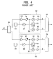
- Fig. 4 shows the configuration of a known dual digital television tuner.
- a digital television intermediate-frequency signal (IF) which is generated by frequency-conversion by an outside downconverter (not shown), is separated and distributed by a distributor 51, and one separated intermediate-frequency signal is input to a first direct conversion circuit 52.
- IF digital television intermediate-frequency signal
- the first direct conversion circuit 52 includes a first intermediate-frequency amplifier 53 to which the one separated intermediate-frequency signal is input, a first variable gain amplifier 54 provided in the next stage, a pair of first mixers 55 and 56 provided in the next stage, a first local oscillator 57 for generating a local oscillation signal, a first phase shifter 58 for dividing the local oscillation signal into two phases orthogonal to each other and for inputting the phases to the mixers 55 and 56, and a pair of first baseband signal amplifiers 59 and 60 provided in the stage after the mixers 55 and 56.
- a first PLL circuit 61 for controlling the oscillation frequency of the first local oscillator 57, a first demodulator 62 for demodulating baseband signals (I/Q), and so forth are provided.
- the second direct conversion circuit 63 includes a second intermediate-frequency amplifier 64 to which the other intermediate-frequency signal is input, a second variable gain amplifier 65 provided in the next stage, a pair of second mixers 66 and 67 provided in the next stage, a second local oscillator 68 for generating a local oscillation signal, a second phase shifter 69 for dividing the local oscillation signal into two phases orthogonal to each other and for inputting the phases to the mixers 66 and 67, and a pair of second baseband signal amplifiers 70 and 71 provided in the stage after the mixers 66 and 67.
- a second PLL circuit 72 for controlling the oscillation frequency of the second local oscillator 68, a second demodulator 73 for demodulating baseband signals (I/Q), and so forth are provided outside the second direct conversion circuit 63.
- the local oscillators 57 and 68 are controlled so that they oscillate at substantially the same frequency as the intermediate frequency of the channel that each of the direct conversion circuits 52 and 63 should receive.
- the pair of mixers 55 and 56 receive local oscillation signals whose phases are orthogonal to each other, and thus the baseband signal amplifiers 59 and 60 output baseband signals which are orthogonal to each other.
- the pair of mixers 66 and 67 receive local oscillation signals whose phases are orthogonal to each other, and thus the baseband signal amplifiers 70 and 71 output baseband signals which are orthogonal to each other.
- the baseband signals are added and demodulated in the demodulators 62 and 73, respectively, converted to an analog signal, and converted to a picture signal or the like.
- the oscillation frequency of the first local oscillator 57 is the same as that of the second local oscillator 68.
- mutual interference between the local oscillation signals causes beating (beating due to a slight difference), leading to a deterioration of the phase noise of the local oscillation signals and degradation of the reception characteristics.
- a dual digital television tuner comprises first and second direct conversion circuits, each having a pair of mixers and a local oscillator, in which a digital television signal is input to the pair of mixers, which directly output baseband signals.
- the first direct conversion circuit comprises one of a frequency divider and a multiplier.
- Each of the pair of mixers, the local oscillator, the frequency divider, and the multiplier is constituted by a balanced circuit.
- An oscillation signal of the local oscillator in the first direct conversion circuit is input to the pair of mixers of the first direct conversion circuit through the frequency divider or the multiplier.
- the difference between the oscillation frequency of the local oscillator of the first direct conversion circuit and that of the local oscillator of the second direct conversion circuit becomes greater and thus interference between the oscillation signals is reduced. Further, even when the frequency of the local oscillation signal input to the pair of mixers of the first direct conversion circuit is the same as that of the local oscillation signal input to the pair of mixers of the second direct conversion circuit, the level of each radiated local oscillation signal is lowered by phase cancellation and the interference can be prevented because both pairs of the mixers are constituted by balanced circuits.
- a dual digital television tuner comprises first and second direct conversion circuits, each having a pair of mixers and a local oscillator, in which a digital television signal is input to the pair of mixers, which directly output baseband signals.
- the first direct conversion circuit comprises a frequency divider and the second direct conversion circuit comprises a multiplier.
- Each of the pair of mixers, the local oscillator, the frequency divider, and the multiplier is constituted by a balanced circuit.
- An oscillation signal of the local oscillator in the first direct conversion circuit is input to the pair of mixers of the first direct conversion circuit through the frequency divider, and an oscillation signal of the local oscillator in the second direct conversion circuit is input to the pair of mixers of the second direct conversion circuit through the multiplier.
- the difference in the frequency of the oscillation signals of the local oscillators becomes greater and mutual interference can be further reduced.
- the oscillation frequency band of the local oscillator in the first direct conversion circuit does not overlap the oscillation frequency band of the local oscillator in the second direct conversion circuit.
- first direct conversion circuit and the second direct conversion circuit may be integrated.
- both pairs of signal input terminals or both pairs of signal output terminals of both pairs of mixers become physically closer to each other and thus radiated local oscillation signals are more likely to be phase-cancelled.
- Fig. 1 is a circuit diagram showing an embodiment.
- a digital television intermediate-frequency signal (IF, see first frequency band A in Fig. 2) of about conversion by an outside downconverter (not shown), is separated and distributed by a distributor 1, and one separated intermediate-frequency signal is input to a first direct conversion circuit 10.
- the first direct conversion circuit 10 is integrated and includes a first intermediate-frequency amplifier 11 to which the one separated intermediate-frequency signal is input, a first variable gain amplifier 12 which is provided in the next stage and which is gain-controlled by an AGC voltage, a pair of first mixers 13 and 14 which are provided in the next stage and which output baseband signals (I signal and Q signal), a first local oscillator 15 for outputting an oscillation signal, a frequency divider 16 for dividing the oscillation frequency of the first local oscillator 15 into 1/N (N is 2, for example), a first phase shifter 17 for dividing the frequency-divided oscillation signal into two phases orthogonal to each other and for inputting the phases as local oscillation signals to the mixers 13 and 14, and a pair of first baseband signal amplifiers 18 and 19 provided in the stage after the mixers 13 and 14.
- Each of the first intermediate-frequency amplifier 11, the first variable gain amplifier 12, the pair of first mixers 13 and 14, the first local oscillator 15, the frequency divider 16, the first phase shifter 17, and the pair of first baseband signal amplifiers 18 and 19 is constituted by a balanced circuit.
- a first PLL circuit 21 for controlling the oscillation frequency of the first local oscillator 15, a first demodulator 22 for demodulating the baseband signals, and so forth are provided.
- the first PLL circuit 21 and the first demodulator 22 are also constituted by balanced circuits.
- the first PLL circuit 21 controls the oscillation frequency of the first local oscillator 15 to be N times the frequency of the intermediate-frequency signal.
- N is 2 and thus the oscillation frequency is 1900 MHz to 4300 MHz (see second frequency band B in Fig. 2).
- baseband signals whose phases are orthogonal to each other are output from the mixers 13 and 14.
- a digital signal generated by demodulation is output from the first demodulator 22 and the digital signal is converted to an analog picture signal and an audio signal by a D/A converter (not shown).
- the other separated intermediate-frequency signal output from the distributor 1 is input to a second direct conversion circuit 30.
- the second direct conversion circuit 30 is also integrated and includes a second intermediate-frequency amplifier 31 to which the other separated intermediate-frequency signal is input, a second variable gain amplifier 32 which is provided in the next stage and which is gain-controlled by an AGC voltage, a pair of second mixers 33 and 34 which are provided in the next stage and which output baseband signals (I signal and Q signal), a second local oscillator 35 for outputting an oscillation signal, a multiplier 36 for multiplying the oscillation frequency of the second local oscillator 35 by M (M is 2, for example), a second phase shifter 37 for dividing the multiplied oscillation signal into two phases which are orthogonal to each other and for inputting the phases as local oscillation signals to the mixers 33 and 34, and a pair of second baseband signal amplifiers 38 and 39 provided in the stage after the mixers 33 and 34.
- Each of the second intermediate-frequency amplifier 31, the second variable gain amplifier 32, the pair of second mixers 33 and 34, the second local oscillator 35, the multiplier 36, the second phase shifter 37, and the pair of second baseband signal amplifiers 38 and 39 is constituted by a balanced circuit.
- a second PLL circuit 41 for controlling the oscillation frequency of the second local oscillator 35, a second demodulator 42 for demodulating the baseband signals, and so forth are provided outside the second direct conversion circuit 30, a second PLL circuit 41 for controlling the oscillation frequency of the second local oscillator 35, a second demodulator 42 for demodulating the baseband signals, and so forth are provided.
- the second PLL circuit 41 and the second demodulator 42 are also constituted by balanced circuits.
- the second PLL circuit 41 controls the oscillation frequency of the second local oscillator 35 to be 1/M times the frequency of the intermediate-frequency signal.
- M is 2 and thus the oscillation frequency is 475 MHz to 1075 MHz (see third frequency band C in Fig. 2).
- baseband signals whose phases are orthogonal to each other are output from the mixers 33 and 34.
- a digital signal generated by demodulation is output from the second demodulator 42 and the digital signal is converted to an analog picture signal and an audio signal by the D/A converter (not shown).
- the division factor N and the multiplication factor M are not limited to identical positive integers as described above, but in general they may be positive rational numbers. By adequately setting the numbers, the oscillation frequency band of the first local oscillator 15 does not overlap that of the second local oscillator 35.
- the frequency of the local oscillation signal input to the first mixers 13 and 14 is the same as the frequency of the local oscillation signal input to the second mixers 33 and 34.
- the region from the frequency divider 16 to the mixers 13 and 14 and the region from the multiplier 36 to the second mixers 33 and 34, where interference is likely to occur are constituted by balanced circuits, and thus radiation of the local oscillation signal from each circuit can be suppressed and interference can be reduced.
- the circuit is naturally miniaturized by integration.
- the frequency divider 16 is provided in the first direct conversion circuit 10 and the multiplier 36 is provided in the second direct conversion circuit 30.
- the above-described advantages are not lost even when the frequency divider 16 of the first direct conversion circuit 10 or the multiplier 36 of the second direct conversion circuit 30 is removed and a frequency divider or a multiplier is provided in any one of the direct conversion circuits.
- a first direct conversion circuit 20 shown in Fig. 3 can be used instead of the first direct conversion circuit 10 shown in Fig. 1.
- the configuration shown in Fig. 3 is the same as that of the direct conversion circuit 10 shown in Fig. 1 except that the direct conversion circuit 20 does not have the frequency divider 16.
- a first local oscillator 25 oscillates within the first frequency band A shown in Fig. 2.
- the oscillation frequency band of the first local oscillator 25 overlaps the oscillation frequency band of the second local oscillator 35 (C in Fig. 2) of the second direct conversion circuit 30 in a narrow range at a higher band, as shown in Fig. 2.
- the possibility is very low, and thus the above-described advantages can be achieved from a practical point of view.
- the oscillation frequency band of the first local oscillator 25 does not overlap the oscillation frequency band of the second local oscillator 35.
Landscapes
- Engineering & Computer Science (AREA)
- Computer Hardware Design (AREA)
- Microelectronics & Electronic Packaging (AREA)
- Superheterodyne Receivers (AREA)
Abstract
Description
- The present invention relates to a dual digital television tuner having two systems.
- Fig. 4 shows the configuration of a known dual digital television tuner. A digital television intermediate-frequency signal (IF), which is generated by frequency-conversion by an outside downconverter (not shown), is separated and distributed by a
distributor 51, and one separated intermediate-frequency signal is input to a firstdirect conversion circuit 52. The firstdirect conversion circuit 52 includes a first intermediate-frequency amplifier 53 to which the one separated intermediate-frequency signal is input, a firstvariable gain amplifier 54 provided in the next stage, a pair offirst mixers local oscillator 57 for generating a local oscillation signal, afirst phase shifter 58 for dividing the local oscillation signal into two phases orthogonal to each other and for inputting the phases to themixers baseband signal amplifiers mixers - Outside the first
direct conversion circuit 52, afirst PLL circuit 61 for controlling the oscillation frequency of the firstlocal oscillator 57, afirst demodulator 62 for demodulating baseband signals (I/Q), and so forth are provided. - On the other hand, the other separated intermediate-frequency signal output from the
distributor 51 is input to a seconddirect conversion circuit 63. The seconddirect conversion circuit 63 includes a second intermediate-frequency amplifier 64 to which the other intermediate-frequency signal is input, a secondvariable gain amplifier 65 provided in the next stage, a pair ofsecond mixers local oscillator 68 for generating a local oscillation signal, asecond phase shifter 69 for dividing the local oscillation signal into two phases orthogonal to each other and for inputting the phases to themixers baseband signal amplifiers mixers - Outside the second
direct conversion circuit 63, asecond PLL circuit 72 for controlling the oscillation frequency of the secondlocal oscillator 68, asecond demodulator 73 for demodulating baseband signals (I/Q), and so forth are provided. - The
local oscillators direct conversion circuits direct conversion circuit 52, the pair ofmixers baseband signal amplifiers - Likewise, in the second
direct conversion circuit 63, the pair ofmixers baseband signal amplifiers - The baseband signals are added and demodulated in the
demodulators - In the above-described configuration, when the first
direct conversion circuit 52 and the seconddirect conversion circuit 63 receive intermediate-frequency signals of the same channel, the oscillation frequency of the firstlocal oscillator 57 is the same as that of the secondlocal oscillator 68. Thus, mutual interference between the local oscillation signals causes beating (beating due to a slight difference), leading to a deterioration of the phase noise of the local oscillation signals and degradation of the reception characteristics. - Accordingly, it is an object of the present invention to provide a dual digital television tuner in which interference between two local oscillation signals can be prevented so that phase noise is reduced.
- To solve the above-described problems, according to a first aspect of the present invention, a dual digital television tuner comprises first and second direct conversion circuits, each having a pair of mixers and a local oscillator, in which a digital television signal is input to the pair of mixers, which directly output baseband signals. The first direct conversion circuit comprises one of a frequency divider and a multiplier. Each of the pair of mixers, the local oscillator, the frequency divider, and the multiplier is constituted by a balanced circuit. An oscillation signal of the local oscillator in the first direct conversion circuit is input to the pair of mixers of the first direct conversion circuit through the frequency divider or the multiplier.
- Accordingly, the difference between the oscillation frequency of the local oscillator of the first direct conversion circuit and that of the local oscillator of the second direct conversion circuit becomes greater and thus interference between the oscillation signals is reduced. Further, even when the frequency of the local oscillation signal input to the pair of mixers of the first direct conversion circuit is the same as that of the local oscillation signal input to the pair of mixers of the second direct conversion circuit, the level of each radiated local oscillation signal is lowered by phase cancellation and the interference can be prevented because both pairs of the mixers are constituted by balanced circuits.
- According to a second aspect of the present invention, a dual digital television tuner comprises first and second direct conversion circuits, each having a pair of mixers and a local oscillator, in which a digital television signal is input to the pair of mixers, which directly output baseband signals. The first direct conversion circuit comprises a frequency divider and the second direct conversion circuit comprises a multiplier. Each of the pair of mixers, the local oscillator, the frequency divider, and the multiplier is constituted by a balanced circuit. An oscillation signal of the local oscillator in the first direct conversion circuit is input to the pair of mixers of the first direct conversion circuit through the frequency divider, and an oscillation signal of the local oscillator in the second direct conversion circuit is input to the pair of mixers of the second direct conversion circuit through the multiplier.
- Accordingly, the difference in the frequency of the oscillation signals of the local oscillators becomes greater and mutual interference can be further reduced.
- Preferably, the oscillation frequency band of the local oscillator in the first direct conversion circuit does not overlap the oscillation frequency band of the local oscillator in the second direct conversion circuit.
- With this arrangement, direct interference between the oscillation signals can be prevented.
- Also, the first direct conversion circuit and the second direct conversion circuit may be integrated.
- Accordingly, both pairs of signal input terminals or both pairs of signal output terminals of both pairs of mixers become physically closer to each other and thus radiated local oscillation signals are more likely to be phase-cancelled.
- An embodiment of the present invention will now be described, by way of example, with reference to the accompanying diagrammatic drawings, in which:
- Fig. 1 is a circuit diagram showing the configuration of a dual digital television tuner according to the present invention;
- Fig. 2 is a frequency band diagram showing each range of local oscillation frequency in the dual digital television tuner according to the present invention;
- Fig. 3 is a circuit diagram showing another configuration of the dual digital television tuner according to the present invention; and
- Fig. 4 is a circuit diagram showing the configuration of a known dual digital television tuner.
-
- Hereinafter, a dual digital television tuner according to the present invention is described with reference to the accompanying drawings. Fig. 1 is a circuit diagram showing an embodiment. A digital television intermediate-frequency signal (IF, see first frequency band A in Fig. 2) of about conversion by an outside downconverter (not shown), is separated and distributed by a distributor 1, and one separated intermediate-frequency signal is input to a first
direct conversion circuit 10. - The first
direct conversion circuit 10 is integrated and includes a first intermediate-frequency amplifier 11 to which the one separated intermediate-frequency signal is input, a firstvariable gain amplifier 12 which is provided in the next stage and which is gain-controlled by an AGC voltage, a pair offirst mixers local oscillator 15 for outputting an oscillation signal, afrequency divider 16 for dividing the oscillation frequency of the firstlocal oscillator 15 into 1/N (N is 2, for example), afirst phase shifter 17 for dividing the frequency-divided oscillation signal into two phases orthogonal to each other and for inputting the phases as local oscillation signals to themixers baseband signal amplifiers mixers - Each of the first intermediate-
frequency amplifier 11, the firstvariable gain amplifier 12, the pair offirst mixers local oscillator 15, thefrequency divider 16, thefirst phase shifter 17, and the pair of firstbaseband signal amplifiers - Outside the first
direct conversion circuit 10, afirst PLL circuit 21 for controlling the oscillation frequency of the firstlocal oscillator 15, afirst demodulator 22 for demodulating the baseband signals, and so forth are provided. Thefirst PLL circuit 21 and thefirst demodulator 22 are also constituted by balanced circuits. - In the configuration described above, a local oscillation signal having the same frequency as that of the channel to be received in the intermediate-frequency signal must be input to the pair of
first mixers mixers frequency divider 16 is N, thefirst PLL circuit 21 controls the oscillation frequency of the firstlocal oscillator 15 to be N times the frequency of the intermediate-frequency signal. In the foregoing case, N is 2 and thus the oscillation frequency is 1900 MHz to 4300 MHz (see second frequency band B in Fig. 2). - Also, baseband signals whose phases are orthogonal to each other are output from the
mixers - A digital signal generated by demodulation is output from the
first demodulator 22 and the digital signal is converted to an analog picture signal and an audio signal by a D/A converter (not shown). - On the other hand, the other separated intermediate-frequency signal output from the distributor 1 is input to a second
direct conversion circuit 30. The seconddirect conversion circuit 30 is also integrated and includes a second intermediate-frequency amplifier 31 to which the other separated intermediate-frequency signal is input, a secondvariable gain amplifier 32 which is provided in the next stage and which is gain-controlled by an AGC voltage, a pair ofsecond mixers local oscillator 35 for outputting an oscillation signal, amultiplier 36 for multiplying the oscillation frequency of the secondlocal oscillator 35 by M (M is 2, for example), asecond phase shifter 37 for dividing the multiplied oscillation signal into two phases which are orthogonal to each other and for inputting the phases as local oscillation signals to themixers baseband signal amplifiers mixers - Each of the second intermediate-
frequency amplifier 31, the secondvariable gain amplifier 32, the pair ofsecond mixers local oscillator 35, themultiplier 36, thesecond phase shifter 37, and the pair of secondbaseband signal amplifiers - Outside the second
direct conversion circuit 30, asecond PLL circuit 41 for controlling the oscillation frequency of the secondlocal oscillator 35, asecond demodulator 42 for demodulating the baseband signals, and so forth are provided. Thesecond PLL circuit 41 and thesecond demodulator 42 are also constituted by balanced circuits. - In the configuration described above, a local oscillation signal having the same frequency as that of the channel to be received in the intermediate-frequency signal must be input to the pair of
second mixers mixers multiplier 36 is M, thesecond PLL circuit 41 controls the oscillation frequency of the secondlocal oscillator 35 to be 1/M times the frequency of the intermediate-frequency signal. In the foregoing case, M is 2 and thus the oscillation frequency is 475 MHz to 1075 MHz (see third frequency band C in Fig. 2). - Also, baseband signals whose phases are orthogonal to each other are output from the
mixers - A digital signal generated by demodulation is output from the
second demodulator 42 and the digital signal is converted to an analog picture signal and an audio signal by the D/A converter (not shown). - In the above case, the oscillation frequency of the first
local oscillator 15 and that of the secondlocal oscillator 35 differ greatly, as is apparent from the comparison between the second frequency band B and the third frequency band C in Fig. 2, and the minimum difference is 825 MHz (=1900 MHz-1075 MHz). Accordingly, the oscillation frequency bands do not overlap each other and direct interference can be prevented. - The division factor N and the multiplication factor M are not limited to identical positive integers as described above, but in general they may be positive rational numbers. By adequately setting the numbers, the oscillation frequency band of the first
local oscillator 15 does not overlap that of the secondlocal oscillator 35. - When the first
direct conversion circuit 10 and the seconddirect conversion circuit 30 receive the intermediate-frequency signal of the same channel, the frequency of the local oscillation signal input to thefirst mixers second mixers frequency divider 16 to themixers multiplier 36 to thesecond mixers first mixers second mixers - In the above case, the
frequency divider 16 is provided in the firstdirect conversion circuit 10 and themultiplier 36 is provided in the seconddirect conversion circuit 30. However, the above-described advantages are not lost even when thefrequency divider 16 of the firstdirect conversion circuit 10 or themultiplier 36 of the seconddirect conversion circuit 30 is removed and a frequency divider or a multiplier is provided in any one of the direct conversion circuits. - For example, a first
direct conversion circuit 20 shown in Fig. 3 can be used instead of the firstdirect conversion circuit 10 shown in Fig. 1. The configuration shown in Fig. 3 is the same as that of thedirect conversion circuit 10 shown in Fig. 1 except that thedirect conversion circuit 20 does not have thefrequency divider 16. In this case, a firstlocal oscillator 25 oscillates within the first frequency band A shown in Fig. 2. As a result, the oscillation frequency band of the firstlocal oscillator 25 overlaps the oscillation frequency band of the second local oscillator 35 (C in Fig. 2) of the seconddirect conversion circuit 30 in a narrow range at a higher band, as shown in Fig. 2. However, the possibility is very low, and thus the above-described advantages can be achieved from a practical point of view. - In this case, too, by adequately setting the multiplication factor M of the
multiplier 36 of the second direct conversion circuit 30 (for example M=3), the oscillation frequency band of the firstlocal oscillator 25 does not overlap the oscillation frequency band of the secondlocal oscillator 35.
Claims (4)
- A dual digital television tuner comprising:wherein the first direct conversion circuit comprises one of a frequency divider and a multiplier,first and second direct conversion circuits, each having a pair of mixers and a local oscillator, in which a digital television signal is input to the pair of mixers, which directly output baseband signals,
each of the pair of mixers, the local oscillator, the frequency divider, and the multiplier is constituted by a balanced circuit, and
an oscillation signal of the local oscillator in the first direct conversion circuit is input to the pair of mixers of the first direct conversion circuit through the frequency divider or the multiplier. - A dual digital television tuner comprising:wherein the first direct conversion circuit comprises a frequency divider and the second direct conversion circuit comprises a multiplier,first and second direct conversion circuits, each having a pair of mixers and a local oscillator, in which a digital television signal is input to the pair of mixers, which directly output baseband signals,
each of the pair of mixers, the local oscillator, the frequency divider, and the multiplier is constituted by a balanced circuit, and
an oscillation signal of the local oscillator in the first direct conversion circuit is input to the pair of mixers of the first direct conversion circuit through the frequency divider, and an oscillation signal of the local oscillator in the second direct conversion circuit is input to the pair of mixers of the second direct conversion circuit through the multiplier. - The dual digital television tuner according to Claim 1, wherein the oscillation frequency band of the local oscillator in the first direct conversion circuit does not overlap the oscillation frequency band of the local oscillator in the second direct conversion circuit.
- The dual digital television tuner according to Claim 1, wherein the first direct conversion circuit and the second direct conversion circuit are integrated.
Applications Claiming Priority (2)
| Application Number | Priority Date | Filing Date | Title |
|---|---|---|---|
| JP2001098859A JP3949389B2 (en) | 2001-03-30 | 2001-03-30 | Dual type digital television tuner |
| JP2001098859 | 2001-03-30 |
Publications (1)
| Publication Number | Publication Date |
|---|---|
| EP1246360A1 true EP1246360A1 (en) | 2002-10-02 |
Family
ID=18952469
Family Applications (1)
| Application Number | Title | Priority Date | Filing Date |
|---|---|---|---|
| EP02251062A Ceased EP1246360A1 (en) | 2001-03-30 | 2002-02-16 | Dual digital television tuner |
Country Status (3)
| Country | Link |
|---|---|
| US (1) | US7002639B2 (en) |
| EP (1) | EP1246360A1 (en) |
| JP (1) | JP3949389B2 (en) |
Cited By (1)
| Publication number | Priority date | Publication date | Assignee | Title |
|---|---|---|---|---|
| EP2088673A1 (en) * | 2008-02-06 | 2009-08-12 | Alps Electric Co., Ltd. | Receiving apparatus |
Families Citing this family (13)
| Publication number | Priority date | Publication date | Assignee | Title |
|---|---|---|---|---|
| US7447491B2 (en) * | 2003-06-06 | 2008-11-04 | Silicon Laboratories Inc. | Multi-tuner integrated circuit architecture utilizing frequency isolated local oscillators and associated method |
| JP2005064764A (en) * | 2003-08-08 | 2005-03-10 | Alps Electric Co Ltd | Direct conversion tuner |
| JP3922235B2 (en) * | 2003-10-14 | 2007-05-30 | 松下電器産業株式会社 | High frequency receiver and integrated circuit used therefor |
| CN101156339A (en) * | 2005-04-07 | 2008-04-02 | Atmel德国有限公司 | Method for interference-free frequency conversion in a receiving system with multiple receivers operating in parallel |
| JP2007124290A (en) * | 2005-10-28 | 2007-05-17 | Alps Electric Co Ltd | Dual type digital television tuner |
| CN101432976A (en) * | 2006-04-24 | 2009-05-13 | 松下电器产业株式会社 | Receiving apparatus, electronic device using the same, and receiving method |
| JP4650554B2 (en) * | 2008-10-22 | 2011-03-16 | ソニー株式会社 | Wireless receiver |
| JP2010109850A (en) * | 2008-10-31 | 2010-05-13 | Sony Corp | Tuner device |
| US20100323636A1 (en) * | 2009-06-23 | 2010-12-23 | Nicholas Cowley | Apparatus and methods for implementing multi-channel tuners |
| US8885106B2 (en) * | 2013-03-13 | 2014-11-11 | Silicon Laboratories Inc. | Multi-tuner using interpolative dividers |
| US9252891B2 (en) | 2013-11-07 | 2016-02-02 | Silicon Laboratories Inc. | Die-to-die communication links for receiver integrated circuit dies and related methods |
| US9160465B2 (en) | 2013-11-07 | 2015-10-13 | Silicon Labortories Inc. | Spur cancellation systems and related methods |
| JP6729059B2 (en) * | 2016-06-24 | 2020-07-22 | 日本電気株式会社 | Relay device, relay system, and relay method |
Citations (3)
| Publication number | Priority date | Publication date | Assignee | Title |
|---|---|---|---|---|
| JPS6367030A (en) * | 1986-09-08 | 1988-03-25 | Hitachi Ltd | receiving device |
| US5285284A (en) * | 1991-11-15 | 1994-02-08 | Kabushiki Kaisha Toshiba | Television receiver with a dual tuner system |
| WO1998032233A2 (en) * | 1997-01-15 | 1998-07-23 | Koninklijke Philips Electronics N.V. | Multi-tuner receiver |
Family Cites Families (12)
| Publication number | Priority date | Publication date | Assignee | Title |
|---|---|---|---|---|
| FR2596220A1 (en) * | 1986-03-21 | 1987-09-25 | Portenseigne | FREQUENCY DEMODULATOR |
| NL8801874A (en) * | 1988-07-26 | 1990-02-16 | Philips Nv | TELEVISION RECEIVER WITH A TUNING CIRCUIT CONTAINING A FREQUENCY SYNTHESIS CIRCUIT. |
| US5140198A (en) * | 1989-08-30 | 1992-08-18 | Seiko Corporation | Image canceling mixer circuit on an integrated circuit chip |
| US5311318A (en) * | 1992-08-17 | 1994-05-10 | Zenith Electronics Corporation | Double conversion digital tuning system using separate digital numbers for controlling the local oscillators |
| US5517685A (en) * | 1993-04-27 | 1996-05-14 | Matsushita Electric Industrial Co., Ltd. | PLL circuit having a multiloop, and FM receiving method and apparatus able to utilize the same |
| JPH08237156A (en) | 1995-02-27 | 1996-09-13 | Matsushita Electric Ind Co Ltd | Television receiver with built-in BS reception function |
| JPH08289212A (en) | 1995-04-14 | 1996-11-01 | Toshiba Corp | Digital / analog shared tuner |
| DE19536527C2 (en) * | 1995-09-29 | 1998-05-07 | Siemens Ag | Receiver architecture for receiving angle-modulated / keyed carrier signals |
| DE19708059A1 (en) * | 1997-02-28 | 1998-09-03 | Philips Patentverwaltung | Sound FM demodulator for sound TV signals and method for sound carrier recognition |
| JPH1141131A (en) * | 1997-07-15 | 1999-02-12 | Toshiba Corp | Wireless communication device |
| JP2001044873A (en) * | 1999-07-29 | 2001-02-16 | Alps Electric Co Ltd | Double frequency converter |
| US6760577B2 (en) * | 2001-03-29 | 2004-07-06 | Maxim Integrated Products, Inc. | Alignment methods and apparatus for I/Q phase and amplitude error correction and image rejection improvement |
-
2001
- 2001-03-30 JP JP2001098859A patent/JP3949389B2/en not_active Expired - Fee Related
-
2002
- 2002-02-16 EP EP02251062A patent/EP1246360A1/en not_active Ceased
- 2002-03-27 US US10/108,592 patent/US7002639B2/en not_active Expired - Fee Related
Patent Citations (3)
| Publication number | Priority date | Publication date | Assignee | Title |
|---|---|---|---|---|
| JPS6367030A (en) * | 1986-09-08 | 1988-03-25 | Hitachi Ltd | receiving device |
| US5285284A (en) * | 1991-11-15 | 1994-02-08 | Kabushiki Kaisha Toshiba | Television receiver with a dual tuner system |
| WO1998032233A2 (en) * | 1997-01-15 | 1998-07-23 | Koninklijke Philips Electronics N.V. | Multi-tuner receiver |
Non-Patent Citations (1)
| Title |
|---|
| PATENT ABSTRACTS OF JAPAN vol. 012, no. 291 (E - 644) 9 August 1988 (1988-08-09) * |
Cited By (1)
| Publication number | Priority date | Publication date | Assignee | Title |
|---|---|---|---|---|
| EP2088673A1 (en) * | 2008-02-06 | 2009-08-12 | Alps Electric Co., Ltd. | Receiving apparatus |
Also Published As
| Publication number | Publication date |
|---|---|
| JP2002300488A (en) | 2002-10-11 |
| US20020140872A1 (en) | 2002-10-03 |
| JP3949389B2 (en) | 2007-07-25 |
| US7002639B2 (en) | 2006-02-21 |
Similar Documents
| Publication | Publication Date | Title |
|---|---|---|
| US7330707B2 (en) | Hetrodyne receiver and IC | |
| JPS5957534A (en) | Indoor unit of receiver for satellite broadcast | |
| JPH0691477B2 (en) | RF tuning circuit | |
| US5898907A (en) | Radio transmitter-receiver adopting both a single frequency and a double frequency conversion | |
| US7002639B2 (en) | Dual digital television tuner | |
| JP5402037B2 (en) | FM / AM demodulator, radio receiver, electronic device, and image correction adjustment method | |
| JPH09270723A (en) | Ic for reception circuit for portable telephone set | |
| JP2002050977A (en) | Receiver circuit and integrated circuit for reception | |
| JPH11112462A (en) | Digital broadcast receiver | |
| JP3725402B2 (en) | Television tuner | |
| JP2001128079A (en) | Fequency converter and high frequency tuner | |
| US5630214A (en) | Wide-band receiving apparatus with local oscillating circuit | |
| US6272312B1 (en) | Satellite broadcasting receiving tuner which inhibits interference caused by satellite broadcast signals having one octave higher frequency band | |
| EP1505731A1 (en) | Direct conversion tuner capable of receiving digital television signals in UHF band and VHF band | |
| US7212794B2 (en) | Receiver with a crystal oscillator having a natural-oscillation frequency set so that a fundamental component and its harmonics are outside the range of a receiving band of a modulated wave signal | |
| JP2000068752A (en) | Digital broadcast receiver | |
| JP3399017B2 (en) | Phase synchronizer | |
| JP2730056B2 (en) | Television tuner | |
| JP2003204263A (en) | Phase locked loop and tuning device | |
| JPH08289221A (en) | Digital / analog shared tuner | |
| JPH07202743A (en) | Frequency converter | |
| JP2001119634A (en) | Satellite broadcasting receiver | |
| JPH10242881A (en) | Digital satellite broadcasting receiver | |
| JP2000224578A (en) | Satellite receiver | |
| JPH11346171A (en) | High frequency signal receiver |
Legal Events
| Date | Code | Title | Description |
|---|---|---|---|
| PUAI | Public reference made under article 153(3) epc to a published international application that has entered the european phase |
Free format text: ORIGINAL CODE: 0009012 |
|
| AK | Designated contracting states |
Kind code of ref document: A1 Designated state(s): AT BE CH CY DE DK ES FI FR GB GR IE IT LI LU MC NL PT SE TR |
|
| AX | Request for extension of the european patent |
Free format text: AL;LT;LV;MK;RO;SI |
|
| 17P | Request for examination filed |
Effective date: 20020808 |
|
| AKX | Designation fees paid |
Designated state(s): DE FR GB |
|
| 17Q | First examination report despatched |
Effective date: 20041228 |
|
| 17Q | First examination report despatched |
Effective date: 20041228 |
|
| STAA | Information on the status of an ep patent application or granted ep patent |
Free format text: STATUS: THE APPLICATION HAS BEEN REFUSED |
|
| 18R | Application refused |
Effective date: 20090710 |