EP1246254A2 - MFOS memory transistor and method of fabricating same - Google Patents
MFOS memory transistor and method of fabricating same Download PDFInfo
- Publication number
- EP1246254A2 EP1246254A2 EP02007061A EP02007061A EP1246254A2 EP 1246254 A2 EP1246254 A2 EP 1246254A2 EP 02007061 A EP02007061 A EP 02007061A EP 02007061 A EP02007061 A EP 02007061A EP 1246254 A2 EP1246254 A2 EP 1246254A2
- Authority
- EP
- European Patent Office
- Prior art keywords
- ferroelectric
- gate
- transistor structure
- oxide
- passivation
- Prior art date
- Legal status (The legal status is an assumption and is not a legal conclusion. Google has not performed a legal analysis and makes no representation as to the accuracy of the status listed.)
- Granted
Links
Images


Classifications
-
- H—ELECTRICITY
- H10—SEMICONDUCTOR DEVICES; ELECTRIC SOLID-STATE DEVICES NOT OTHERWISE PROVIDED FOR
- H10D—INORGANIC ELECTRIC SEMICONDUCTOR DEVICES
- H10D30/00—Field-effect transistors [FET]
- H10D30/60—Insulated-gate field-effect transistors [IGFET]
-
- H—ELECTRICITY
- H10—SEMICONDUCTOR DEVICES; ELECTRIC SOLID-STATE DEVICES NOT OTHERWISE PROVIDED FOR
- H10D—INORGANIC ELECTRIC SEMICONDUCTOR DEVICES
- H10D64/00—Electrodes of devices having potential barriers
- H10D64/60—Electrodes characterised by their materials
- H10D64/66—Electrodes having a conductor capacitively coupled to a semiconductor by an insulator, e.g. MIS electrodes
- H10D64/68—Electrodes having a conductor capacitively coupled to a semiconductor by an insulator, e.g. MIS electrodes characterised by the insulator, e.g. by the gate insulator
- H10D64/689—Electrodes having a conductor capacitively coupled to a semiconductor by an insulator, e.g. MIS electrodes characterised by the insulator, e.g. by the gate insulator having ferroelectric layers
-
- H—ELECTRICITY
- H10—SEMICONDUCTOR DEVICES; ELECTRIC SOLID-STATE DEVICES NOT OTHERWISE PROVIDED FOR
- H10D—INORGANIC ELECTRIC SEMICONDUCTOR DEVICES
- H10D30/00—Field-effect transistors [FET]
- H10D30/60—Insulated-gate field-effect transistors [IGFET]
- H10D30/701—IGFETs having ferroelectric gate insulators, e.g. ferroelectric FETs
-
- H—ELECTRICITY
- H10—SEMICONDUCTOR DEVICES; ELECTRIC SOLID-STATE DEVICES NOT OTHERWISE PROVIDED FOR
- H10D—INORGANIC ELECTRIC SEMICONDUCTOR DEVICES
- H10D64/00—Electrodes of devices having potential barriers
- H10D64/01—Manufacture or treatment
- H10D64/031—Manufacture or treatment of data-storage electrodes
- H10D64/033—Manufacture or treatment of data-storage electrodes comprising ferroelectric layers
Definitions
- This invention relates generally to semiconductor technology and more particularly to metal-ferroelectric-insulator semiconductor (MFIS) transistor structures, and methods of fabrication.
- MFIS transistor is similar to an MFOS transistor, but is not limited to structures that use oxide as the insulator material.
- ferroelectric electrode stack comprising a ferroelectric gate with a top electrode.
- the device would be formed by depositing a ferroelectric material, followed by an overlying metal layer. The layers would then be plasma etched. Plasma etching degrades the ferroelectric properties of the ferroelectric gate, thereby reducing the reliability of the memory transistor.
- the ferroelectric material also needed to be passivated to prevent contamination from hydrogen. Passivation was also used to reduce unwanted interactions between the ferroelectric material and underlying oxide.
- a ferroelectric transistor structure comprising a ferroelectric gate overlying a semiconductor substrate.
- the ferroelectric gate has a bottom with a gate dielectric interposed between the bottom and the semiconductor substrate.
- the ferroelectric gate also has sides with adjacent passivation sidewalls, and a top covered with a top electrode.
- the top electrode, the passivation sidewalls and the gate dielectric serve to encapsulate the ferroelectric gate, thereby reducing, or eliminating, contamination due to oxygen, hydrogen or other contaminants.
- a method of forming the ferroelectric gate structure of the present invention is also provided.
- a gate insulation material is formed over the substrate.
- a sacrificial gate structure is formed overlying the gate insulation material and removed to produce an open gate region.
- a passivation insulator is deposited over the substrate, including the open gate region. The passivation insulator is anisotropic plasma etched to form passivation sidewalls.
- a ferroelectric material is deposited over the substrate including the open gate region and then polished using CMP.
- a top electrode is then formed over the remaining ferroelectric material. The combination of the top electrode, the passivation side walls and the gate insulation serve to encapsulate and protected the ferroelectric material.
- the gate insulator is preferably ZrO 2 , zirconium silicate, Zr-Al-Si-O, HfO 2 , hafnium silicate, Hf-Al-O, La-Al-O, lanthanum oxide Ta 2 O 5 , or other suitable high-k material
- the gate insulator may also be silicon nitride, nitrogen implanted silicon dioxide, or silicon oxynitride.
- the passivation sidewalls are preferably TiO 2 , Al 2 O 3 , TiAlO x , or Si 3 N 4
- the ferroelectric material is preferably PGO, PZT, SBT, SBO, SBTO, SBTN, STO, BTO, BLT, LNO, YMnO 3 , or other suitable material.
- the top electrode is preferably iridium, platinum, ruthenium, iridium oxide, platinum oxide, ruthenium oxide, or other suitable material.
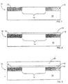
- Fig. 1 shows a semiconductor structure 10 that has been prepared using state of the art processes. Shallow trench isolation (STI) has been used to produce isolation regions 12, and an active device region 14 on a substrate 16. Although an STI structure is shown, it would also be possible to use LOCOS isolation instead of STI.
- the semiconductor substrate is preferably silicon or silicon on insulator (SOI).
- Fig. 2 shows the semiconductor structure 10 following formation of a gate insulation material 18, which may also be referred to as the gate dielectric.
- the gate insulation material 18 is a metal oxide that does not react significantly with a ferroelectric material to be deposited in subsequent steps.
- the gate insulation material may be silicon dioxide, nitrogen implanted silicon dioxide, silicon nitride or silicon oxynitride, the gate insulation material 18 is preferably a high-k material.
- Zirconium oxide (ZrO 2 ) is currently the preferred material.
- ZrO 2 is preferred, other suitable high-k materials including, zirconium silicate, Zr-Al-Si-O, HfO 2 , hafnium silicate, Hf-Al-O, La-Al-Q, lanthanum oxide and Ta 2 O 5 may be used.
- the gate insulation material 18 is preferably deposited to an equivalent thermal oxide thickness of between 0.5nm and 10nm.
- the equivalent thermal oxide thickness may have an actual thickness greater than that of silicon dioxide due to higher dielectric constants associated with these materials.
- the gate insulation material is preferably deposited to a thickness of between approximately 1nm and 100nm.
- the gate insulation material 18 can be grown thermally and subsequently implanted as desired.
- the available deposition methods include chemical vapor deposition, including pulsed CVD, sputtering, or evaporation.
- ZrO 2 may be deposited using atomic layer deposition, also referred to as "pulsed CVD".
- Atomic layer deposition is used to deposit an extremely thin layer of material onto the substrate.
- Atomic layer deposition employs a chemical phenomenon known as chemisorption. In chemisorption, a material in a gas phase will adsorb to a surface saturating it, forming a monolayer.
- Most conventional deposition techniques employ physisorption processes, which produce multilayer deposition regions with a surface coverage that is purely statistical. By taking advantage of chemisorption, films can be grown that are extremely uniform in thickness and composition.
- ZrO 2 films have reportedly been grown this way on silicon by using zirconium chloride (ZrCl 4 ) to form the first monolayer, purging the system of ZrCl 4 , and then exposing the surface to water vapor (H 2 O).
- Other precursors for producing zirconium oxide layers include zirconium propoxide (Zr(iOPr) 4 ) and zirconium tetramethyl heptanedionato (Zr(tmhd) 4 ). Chemisorption occurs over a very limited range of temperature and pressures for a given gas-solid combination.
- zirconium oxide has reportedly been deposited on silicon substrates at a temperature of 300 degrees Celsius using ZrCl 4 and H 2 O. As the process produces a monolayer, thicker layers of zirconium oxide would be produced by adding additional monolayers.
- ZrO 2 may also be deposited using the precursors identified above, as well as other precursors, in a more conventional CVD process.
- An alternative deposition technique using conventional systems is to sputter targets to lay down a thin layer of high-k material.
- a sputtering target of high purity metal is used.
- a wafer is prepared and placed into a deposition chamber. The wafer is then heated to a temperature between room temperature and 500 degrees Celsius.
- a mixture of argon (Ar) and oxygen (O 2 ) is then introduced into the deposition chamber.
- a plasma with a sputtering power of between approximately 500 W and 5kW is produced within the chamber.
- the zirconium shutter is opened to deposit zirconium over the wafer, and then closed. The presence of oxygen within the chamber will cause the target material to form ZrO 2 concurrently with the deposition on the wafer
- evaporation of targets is used to deposit the thin layer.
- the basic process is substantially identical to the description provided above with regard to sputtering, except that instead of exposing the targets to a plasma, the targets are heated to a temperature of between approximately 1,000 and 2,000 degrees Celsius.
- shutters can be used to control the duration of the deposition.
- Fig. 3 shows a sacrificial layer 20 deposited overlying the gate insulation material 18.
- the sacrificial layer is deposited to a thickness of between approximately 200nm and 400nm.
- the sacrificial layer is preferably silicon nitride or polysilicon.
- the sacrificial layer is preferably easy to remove by selective etching without affecting underlying or adjacent materials.
- Fig. 4 shows a sacrificial gate structure 22 formed by patterning the sacrificial layer using an overlying mask layer (not shown), and plasma etching the sacrificial layer.
- the plasma etch may stop at the gate insulation material.
- the plasma etch may partially, or completely, remove the gate insulation material from areas not covered by the mask pattern.
- a source region 24 and a drain region 26 are formed adjacent to the sacrificial gate structure 22.
- the source region 24 and the drain region 26 may be formed by any state of the art process, but preferably by ion implantation.
- Fig. 5 shows the semiconductor structure 10 following deposition of an oxide layer 30.
- the oxide layer 30 is deposited overlying the sacrificial gate structure and surrounding regions.
- the oxide layer 30 is deposited to a thickness at which the lowest portion of the oxide is at least as high as the sacrificial gate structure 22. This thickness is preferably 1 to 2 times the height of the sacrificial gate structure 22 above the substrate 16.
- CMP chemical-mechanical polishing
- the CMP process is preferably stopped at the top of the sacrificial gate structure 22, without removing a significant portion of the sacrificial gate structure 22.
- Fig. 6 shows the semiconductor structure 10 following removal of the sacrificial gate structure.
- the removal of the sacrificial gate structure leaves an open gate region 32.
- the sacrificial gate structure is preferably removed using a wet etch process.
- Fig. 7 shows the semiconductor structure 10 following deposition of a passivation insulator 34.
- the passivation insulator 34 is preferably selected from materials that will reduce, or eliminate, diffusion of oxygen or hydrogen through it. Preferred materials for forming the passivation insulator 34 are TiO 2 , Al 2 O 3 , TiAlO x , and Si 3 N 4 .
- the passivation insulator 34 may be deposited by sputtering or other suitable method known to one of ordinary skill in the art.
- Fig. 8 shows the semiconductor structure 10 following anisotropic plasma etching of the passivation insulator 34.
- the anisotropic etch removes the passivation insulator 34 from horizontal surfaces, leaving passivation sidewalls 36.
- Fig. 9 shows the semiconductor structure 10 following deposition of a ferroelectric material 38.
- the ferroelectric material fills the open gate region.
- the ferroelectric material 38 is deposited to a thickness greater than the depth of the open gate region.
- the ferroelectric material 38 may be deposited by metal-organic chemical vapor deposition (MOCVD) or a chemical-solution deposition (CSD) process.
- MOCVD metal-organic chemical vapor deposition
- CSD chemical-solution deposition
- the ferroelectric material is preferably selected from PGO, PZT, SBT, SBO, SBTO, SBTN, STO, BTO, BLT, LNO, and YMnO 3 .
- a PGO material which may also be referred to as Pb 5 Ge 3 O 11 , may be deposited using the following preferred method.
- the PGO material is deposited by metal organic vapor deposition (MOCVD) and RTP(Rapid Thermal Process) annealing techniques.
- the PGO material may be deposited at temperatures between 450 and 550°C.
- An EMCORE oxide MOCVD reactor with liquid delivery system was used for the growth of PGO material.
- the precursors for the PGO material are listed in Table 1.
- the properties of precursors for PGO thin films Precursors Formula Vapor Pressure (mm Hg) Decomposition Temperature (°C) Pb(thd) 2 Ge(ETO) 4 Pb(C 11 H 19 O 2 ) 2 Ge(C 2 H 5 O) 4 180°C/0.05 b.p. 185.5°C 325°C
- Liquid precursors such as germanium alkoxides, germanium halides, lead alkyls, and lead halides use a bubbler with a controlled temperature to generate precursor vapors.
- Solid precursors such as lead ⁇ -diketonates, are dissolved in a solvent and use a liquid delivery system coupled with a flash vaporizer to generate precursor vapors.
- Table 2 is a list of PGO precursors that may be used in some aspects of the present invention.
- the properties of precursors for PGO films Precursor Formula Appearance at room temperature Moisture stability Vapor Pressure (mm Hg) Decomposition Temp.
- Table 3 is a list of solvents that are alternately available for use in some aspects of the present invention.
- the properties of solvents for PGO films Solvents Formula Boiling Temp. (°C) Tetrahydrofuran (THF) C 4 H 8 O 65 - 67 °C Iso-propanol C 3 H 7 OH 97 °C Tetraglyme C 10 H 22 O 5 275 °C Xylene C 6 H 4 (CH 3 ) 2 137 - 144 °C Toluene C 6 H 5 CH 3 111 °C Butyl ether [CH 3 (CH 2 ) 3 ] 2 O 142 - 143°C Butyl acetate CH 3 CO 2 (CH 2 ) 3 CH 3 124 - 126 °C 2-Ethyl-1-hexanol CH 3 (CH 2 ) 3 CH(C 2 H 6 )CH 2 183 - 186°C OH
- [Pb(thd) 2 ] and [Ge(ETO) 4 ] with a molar ratio of 5:3 were dissolved in a mixed solvent of tetrahydrofuran, isopropanol and tetraglyme in the molar ratio of 8:2:1.
- the precursor solutions have a concentration of 0.1 to 0.3 M/L of Pb 5 Ge 3 O 11 .
- the solution was injected into a vaporizer (150°C) by a pump at a rate of 0.1 ml/min to form precursor gases.
- the precursor gases were brought into the reactor using a preheated argon flow at 150 - 170°C.
- the deposition temperatures and pressure are 500°C and 5 - 10 Torr separately.
- the shroud flow (Ar 4000 sccm) with oxygen (1000 - 2000 sccm) was led into the reactor. After deposition, the PGO material was cooled down to room temperature in an oxygen atmosphere. The PGO material may be annealed using RTP.
- CSD process may be used to deposit the ferroelectric material instead of MOCVD.
- One form of CSD process is a spin on method.
- a PGO thin film may be deposited using the spin on method.
- the precursors are lead acetate and germanium iopropoxide in di (ethylene glycol) ethyl ether solution.
- the precursors are spun over the substrate and any overlying structures forming a film.
- the film is baked at 50 to 350 degrees Celsius for 1 to 10 minutes and pre-annealed after each spin coating at 400 to 500 degrees Celsius for 1 to 15 minutes to evaporate the solvent and eliminate the organic components.
- Each spin coating layer has a thickness of between about 10nm and 100nm.
- the PGO film can be produced with a desired thickness.
- the PGO film is crystallized at 500 to 600 degrees Celsius for 5 minutes to 3 hours in oxygen ambient. Optimization of the process can be achieved for a desired film thickness, without undue experimentation.
- Fig. 10 shows the semiconductor structure 10 following CMP of the ferroelectric material to produce a ferroelectric gate 40.
- the CMP process preferably stops at the top of the passivation sidewalls 36.
- the CMP process may extend slightly below the top of the passivation sidewalls 36.
- Fig. 11 shows the semiconductor structure 10 following deposition of an electrode layer 42.
- the electrode layer 42 comprises iridium, platinum, ruthenium, or their oxides.
- the electrode layer 42 is patterned and etched to form a top electrode 44, as shown in Fig. 12.
- the electrode layer 42 may be patterned using photoresist or a hard mask material, such as TiN, TiO 2 , TiAlO 3 , SiO 2 , SiN, or other suitable material.
- the electrode layer may be etched by plasma etching or other suitable etching process.
- an inlaid, or damascene, method may be used to form the top electrode 44.
- a trench would be formed using a method similar to that used in forming the ferroelectric gate, which was described in detail above.
- a metal such as iridium, platinum, ruthenium, or their oxides, would then be deposited into the trench and polished using CMP to form the top electrode 44.
- Fig. 12 shows the semiconductor structure 10 with a ferroelectric gate structure 46.
- the ferroelectric gate structure 46 comprises the ferroelectric gate 40 protected by the gate insulation material 18 below, the passivation sidewalls 36 along the sides, and the top electrode 44 above. This will reduce, or eliminate, contamination of the ferroelectric gate 40 from oxygen or hydrogen diffusing into the ferroelectric gate 40.
- Fig. 13 shows the semiconductor structure 10 with a passivation layer 48 deposited overlying the ferroelectric gate structure 46.
- Fig. 14 shows the semiconductor structure 10 following final metallization using state of the art methods. Connections 50 to the source region 24, the drain region 26, and the top electrode 44 are shown as simplified structures. Any state of the art metallization scheme may be used, including copper metallization. The metallization may include barrier layers and other layers that are used in connection with various metallization schemes.
- damascene metallization process instead of copper metallization.
Landscapes
- Semiconductor Memories (AREA)
- Non-Volatile Memory (AREA)
- Physical Vapour Deposition (AREA)
- Chemical Vapour Deposition (AREA)
- Formation Of Insulating Films (AREA)
Abstract
Description
| The properties of precursors for PGO thin films | |||
| Precursors | Formula | Vapor Pressure (mm Hg) | Decomposition Temperature (°C) |
| Pb(thd)2 Ge(ETO)4 | Pb(C11H19O2)2 Ge(C2H5O)4 | 180°C/0.05 b.p. 185.5°C | 325°C |
| The properties of precursors for PGO films | |||||
| Precursor | Formula | Appearance at room temperature | Moisture stability | Vapor Pressure (mm Hg) | Decomposition Temp. (°C) |
| GeH4 | |||||
| Ge2H6 | |||||
| Ge3H8 | |||||
| Ge(ETO)4 | Ge(OC2H5)4 | colorless liquid | sensitive | 185°C | |
| GeCl4 | |||||
| (C2H5)2GeCl2 | |||||
| Pb | Pb(C6H5)4 | white | 230° | 325°C | |
| Tetraphenyl | powder | C/0.05 | |||
| Pb(thd)2 | Pb(C11H19O2)2 | white | 180° | 325°C | |
| powder | C/0.05 | ||||
| Pb(C2H5)4 |
| The properties of solvents for PGO films | ||
| Solvents | Formula | Boiling Temp. (°C) |
| Tetrahydrofuran (THF) | C4H8O | 65 - 67 °C |
| Iso-propanol | C3H7OH | 97 °C |
| Tetraglyme | C10H22O5 | 275 °C |
| Xylene | C6H4(CH3)2 | 137 - 144 °C |
| Toluene | C6H5CH3 | 111 °C |
| Butyl ether | [CH3(CH2)3]2O | 142 - 143°C |
| Butyl acetate | CH3CO2(CH2)3CH3 | 124 - 126 °C |
| 2-Ethyl-1-hexanol | CH3(CH2)3CH(C2H6)CH2 | 183 - 186°C |
| OH |
Claims (30)
- A ferroelectric transistor structure comprising:a) a ferroelectric gate having a bottom, sides and a top overlying a semiconductor substrate;b) a gate insulator interposed between the ferroelectric gate and the semiconductor substrate; andc) passivation sidewalls adjacent the sides.
- The ferroelectric transistor structure of claim 1, wherein the semiconductor substrate is silicon or SOI.
- The ferroelectric transistor structure of claim 1, wherein the ferroelectric gate is PGO, PZT, SBT, SBO, SBTO, SBTN, STO, BTO, BLT, LNO or YMnO3.
- The ferroelectric transistor structure of claim 1, wherein the gate insulator is silicon nitride, nitrogen implanted silicon oxide, or silicon oxynitride.
- The ferroelectric transistor structure of claim 1, wherein the gate insulator is ZrO2, zirconium silicate, Zr-Al-Si-O, HfO2, hafnium silicate, Hf-Al-O, La-Al-O, lanthanum oxide or Ta2O5.
- The ferroelectric transistor structure of claim 1, wherein the ferroelectric gate is deposited using a chemical-solution deposition (CSD) method.
- The ferroelectric transistor structure of claim 1, wherein the passivation sidewalls comprise TiO2, Al2O3, TiAlOx, or Si3N4.
- The ferroelectric transistor structure of claim 1, further comprising a top electrode overlying the ferroelectric gate.
- The ferroelectric transistor structure of claim 8, wherein the top electrode comprises iridium, platinum, ruthenium, iridium oxide, platinum oxide, or ruthenium oxide.
- A ferroelectric transistor structure comprising a ferroelectric gate having a bottom, sides and a top, overlying a semiconductor substrate, wherein the ferroelectric gate is encapsulated by the combination of a gate insulator on the bottom, passivation sidewalls on the sides, and a top electrode on the top.
- The ferroelectric transistor structure of claim 10, wherein the semiconductor substrate is silicon or SOI.
- The ferroelectric transistor structure of claim 10, wherein the ferroelectric gate is PGO, PZT, SBT, SBO, SBTO, SBTN, STO, BTO, BLT, LNO or YMnO3.
- The ferroelectric transistor structure of claim 10, wherein the gate insulator is ZrO2, zirconium silicate, Zr-Al-Si-O, HfO2, hafnium silicate, Hf-Al-O, La-Al-O, lanthanum oxide or Ta2O5.
- The ferroelectric transistor structure of claim 10, wherein the ferroelectric gate is deposited using a chemical-solution deposition (CSD) method.
- The ferroelectric transistor structure of claim 10, wherein the top electrode comprises iridium, platinum, ruthenium, iridium oxide, platinum oxide, or ruthenium oxide.
- The ferroelectric transistor structure of claim 10, wherein the passivation sidewalls comprise TiO2, Al2O3, TiAlOx, or Si3N4.
- The ferroelectric transistor structure of claim 10, wherein the gate insulator is silicon nitride, nitrogen implanted silicon oxide, or silicon oxynitride.
- A method of forming a ferroelectric transistor structure on a substrate comprising the steps of:a) forming a gate insulator over the substrate;b) producing a sacrificial gate structure overlying the substrate;c) removing the sacrificial gate structure;d) depositing a passivation insulator over the substrate;e) etching the passivation insulator using anisotropic etching, whereby passivation sidewalls are formed;f) depositing a ferroelectric material over the substrate;g) polishing the ferroelectric material using chemical-mechanical polishing (CMP), whereby a ferroelectric gate is formed; andh) forming a top electrode overlying the ferroelectric gate.
- The method of claim 18, wherein the step of forming the sacrificial gate accomplished by the steps of:a) depositing and patterning a layer of sacrificial gate material, whereby a sacrificial gate is formed;b) forming an oxide overlying the sacrificial gate;c) and polishing the oxide to expose the sacrificial gate.
- The method of claim 19, wherein the layer of sacrificial gate material is silicon nitride or polysilicon.
- The method of claim 19, wherein the step of polishing is accomplished using chemical-mechanical polishing (CMP).
- The method of claim 18, wherein the step of depositing the gate insulator is accomplished by chemical vapor deposition (CVD), pulsed CVD, sputtering, or evaporation.
- The method of claim 18, wherein the step of depositing the gate insulator deposits ZrO2, zirconium silicate, Zr-Al-Si-O, HfO2, hafnium silicate, Hf-Al-O, La-Al-O, lanthanum oxide or Ta2O5.
- The method of claim 18, wherein the step of depositing the ferroelectric material is accomplished by metal-organic chemical vapor deposition (MOCVD), or chemical-solution deposition (CSD).
- The method of claim 18, wherein the step of depositing the ferroelectric material deposits PGO, PZT, SBT, SBO, SBTO, SBTN, STO, BTO, BLT, LNO or YMnO3.
- The method of claim 18, wherein the top electrode is iridium, platinum, iridium oxide or platinum oxide.
- The method of claim 18, wherein the step of forming the top electrode is accomplished by depositing and patterning a top electrode layer.
- The method of claim 18, wherein the step of forming the top electrode is accomplished by using a damascene process.
- The method of claim 18, wherein the step of depositing the passivation insulator deposits TiO2, Al2O3, TiAlOx, or Si3N4.
- The method of claim 18, wherein the step of etching the passivation insulator is accomplished using anisotropic plasma etch.
Applications Claiming Priority (2)
| Application Number | Priority Date | Filing Date | Title |
|---|---|---|---|
| US09/820,039 US6531324B2 (en) | 2001-03-28 | 2001-03-28 | MFOS memory transistor & method of fabricating same |
| US820039 | 2004-04-08 |
Publications (3)
| Publication Number | Publication Date |
|---|---|
| EP1246254A2 true EP1246254A2 (en) | 2002-10-02 |
| EP1246254A3 EP1246254A3 (en) | 2004-10-20 |
| EP1246254B1 EP1246254B1 (en) | 2006-10-25 |
Family
ID=25229720
Family Applications (1)
| Application Number | Title | Priority Date | Filing Date |
|---|---|---|---|
| EP02007061A Expired - Lifetime EP1246254B1 (en) | 2001-03-28 | 2002-03-27 | MFOS memory transistor and method of fabricating same |
Country Status (6)
| Country | Link |
|---|---|
| US (2) | US6531324B2 (en) |
| EP (1) | EP1246254B1 (en) |
| JP (1) | JP3909753B2 (en) |
| KR (1) | KR100479517B1 (en) |
| DE (1) | DE60215571T2 (en) |
| TW (1) | TW535288B (en) |
Cited By (2)
| Publication number | Priority date | Publication date | Assignee | Title |
|---|---|---|---|---|
| FR2849531A1 (en) * | 2002-12-27 | 2004-07-02 | St Microelectronics Sa | METHOD OF FORMING A LOCALIZED REGION OF A DIFFICULTALLY ENGRAVABLE MATERIAL |
| WO2004077574A3 (en) * | 2003-02-28 | 2004-11-18 | Infineon Technologies Ag | Semiconductor memory cell and method for producing said cell |
Families Citing this family (62)
| Publication number | Priority date | Publication date | Assignee | Title |
|---|---|---|---|---|
| US5976928A (en) * | 1997-11-20 | 1999-11-02 | Advanced Technology Materials, Inc. | Chemical mechanical polishing of FeRAM capacitors |
| US7554829B2 (en) | 1999-07-30 | 2009-06-30 | Micron Technology, Inc. | Transmission lines for CMOS integrated circuits |
| US20020104993A1 (en) * | 2000-08-07 | 2002-08-08 | Fitzgerald Eugene A. | Gate technology for strained surface channel and strained buried channel MOSFET devices |
| GB0024294D0 (en) * | 2000-10-04 | 2000-11-15 | Univ Cambridge Tech | Solid state embossing of polymer devices |
| US6852167B2 (en) | 2001-03-01 | 2005-02-08 | Micron Technology, Inc. | Methods, systems, and apparatus for uniform chemical-vapor depositions |
| WO2002103760A2 (en) * | 2001-06-14 | 2002-12-27 | Amberware Systems Corporation | Method of selective removal of sige alloys |
| TW512463B (en) * | 2001-09-28 | 2002-12-01 | Macronix Int Co Ltd | Method for epitaxial growth of lead zirconate titanate film |
| US6664116B2 (en) * | 2001-12-12 | 2003-12-16 | Sharp Laboratories Of America, Inc. | Seed layer processes for MOCVD of ferroelectric thin films on high-k gate oxides |
| JP3581354B2 (en) * | 2002-03-27 | 2004-10-27 | 株式会社東芝 | Field effect transistor |
| US7589029B2 (en) | 2002-05-02 | 2009-09-15 | Micron Technology, Inc. | Atomic layer deposition and conversion |
| US7045430B2 (en) * | 2002-05-02 | 2006-05-16 | Micron Technology Inc. | Atomic layer-deposited LaAlO3 films for gate dielectrics |
| US7160577B2 (en) | 2002-05-02 | 2007-01-09 | Micron Technology, Inc. | Methods for atomic-layer deposition of aluminum oxides in integrated circuits |
| TW554524B (en) * | 2002-05-28 | 2003-09-21 | Univ Nat Chiao Tung | Manufacturing method of ferrolectric FET |
| US7135421B2 (en) | 2002-06-05 | 2006-11-14 | Micron Technology, Inc. | Atomic layer-deposited hafnium aluminum oxide |
| US6884739B2 (en) | 2002-08-15 | 2005-04-26 | Micron Technology Inc. | Lanthanide doped TiOx dielectric films by plasma oxidation |
| JP4887481B2 (en) | 2002-08-20 | 2012-02-29 | 独立行政法人産業技術総合研究所 | Semiconductor ferroelectric memory device |
| US7199023B2 (en) | 2002-08-28 | 2007-04-03 | Micron Technology, Inc. | Atomic layer deposited HfSiON dielectric films wherein each precursor is independendently pulsed |
| US7084078B2 (en) | 2002-08-29 | 2006-08-01 | Micron Technology, Inc. | Atomic layer deposited lanthanide doped TiOx dielectric films |
| US6958302B2 (en) | 2002-12-04 | 2005-10-25 | Micron Technology, Inc. | Atomic layer deposited Zr-Sn-Ti-O films using TiI4 |
| US7101813B2 (en) | 2002-12-04 | 2006-09-05 | Micron Technology Inc. | Atomic layer deposited Zr-Sn-Ti-O films |
| JP2004245660A (en) * | 2003-02-13 | 2004-09-02 | Seiko Instruments Inc | Manufacture of chip sample, and method and system for observing wall surface of the same |
| US7192892B2 (en) | 2003-03-04 | 2007-03-20 | Micron Technology, Inc. | Atomic layer deposited dielectric layers |
| US7135369B2 (en) * | 2003-03-31 | 2006-11-14 | Micron Technology, Inc. | Atomic layer deposited ZrAlxOy dielectric layers including Zr4AlO9 |
| US7220665B2 (en) * | 2003-08-05 | 2007-05-22 | Micron Technology, Inc. | H2 plasma treatment |
| KR100543528B1 (en) * | 2003-08-26 | 2006-01-31 | 한국과학기술연구원 | Fabrication method of self-aligned ferroelectric gate transistor using buffer layer with high etching selectivity |
| JP4212435B2 (en) * | 2003-08-29 | 2009-01-21 | 株式会社東芝 | Semiconductor device and manufacturing method thereof |
| KR101036159B1 (en) * | 2003-11-20 | 2011-05-23 | 매그나칩 반도체 유한회사 | Metal wiring formation method using dual damascene method |
| US7662689B2 (en) * | 2003-12-23 | 2010-02-16 | Intel Corporation | Strained transistor integration for CMOS |
| US7008833B2 (en) * | 2004-01-12 | 2006-03-07 | Sharp Laboratories Of America, Inc. | In2O3thin film resistivity control by doping metal oxide insulator for MFMox device applications |
| US6995025B2 (en) * | 2004-06-21 | 2006-02-07 | Sharp Laboratories Of America, Inc. | Asymmetrical programming ferroelectric memory transistor |
| KR100741983B1 (en) | 2004-07-05 | 2007-07-23 | 삼성전자주식회사 | Semiconductor device having a gate insulating layer of a high dielectric constant and method of manufacturing the same |
| US7601649B2 (en) | 2004-08-02 | 2009-10-13 | Micron Technology, Inc. | Zirconium-doped tantalum oxide films |
| US7378286B2 (en) * | 2004-08-20 | 2008-05-27 | Sharp Laboratories Of America, Inc. | Semiconductive metal oxide thin film ferroelectric memory transistor |
| US7081421B2 (en) | 2004-08-26 | 2006-07-25 | Micron Technology, Inc. | Lanthanide oxide dielectric layer |
| US7494939B2 (en) | 2004-08-31 | 2009-02-24 | Micron Technology, Inc. | Methods for forming a lanthanum-metal oxide dielectric layer |
| US7588988B2 (en) | 2004-08-31 | 2009-09-15 | Micron Technology, Inc. | Method of forming apparatus having oxide films formed using atomic layer deposition |
| JP4785180B2 (en) | 2004-09-10 | 2011-10-05 | 富士通セミコンダクター株式会社 | Ferroelectric memory, multilevel data recording method, and multilevel data reading method |
| US20060060930A1 (en) * | 2004-09-17 | 2006-03-23 | Metz Matthew V | Atomic layer deposition of high dielectric constant gate dielectrics |
| US6991942B1 (en) * | 2004-09-28 | 2006-01-31 | Sharp Laboratories Of America, Inc. | MFIS ferroelectric memory array on SOI and method of making same |
| US7235501B2 (en) | 2004-12-13 | 2007-06-26 | Micron Technology, Inc. | Lanthanum hafnium oxide dielectrics |
| US7560395B2 (en) | 2005-01-05 | 2009-07-14 | Micron Technology, Inc. | Atomic layer deposited hafnium tantalum oxide dielectrics |
| US7687409B2 (en) | 2005-03-29 | 2010-03-30 | Micron Technology, Inc. | Atomic layer deposited titanium silicon oxide films |
| US7662729B2 (en) | 2005-04-28 | 2010-02-16 | Micron Technology, Inc. | Atomic layer deposition of a ruthenium layer to a lanthanide oxide dielectric layer |
| US7572695B2 (en) | 2005-05-27 | 2009-08-11 | Micron Technology, Inc. | Hafnium titanium oxide films |
| US20060278339A1 (en) * | 2005-06-13 | 2006-12-14 | Lam Research Corporation, A Delaware Corporation | Etch rate uniformity using the independent movement of electrode pieces |
| US7927948B2 (en) | 2005-07-20 | 2011-04-19 | Micron Technology, Inc. | Devices with nanocrystals and methods of formation |
| US7410910B2 (en) | 2005-08-31 | 2008-08-12 | Micron Technology, Inc. | Lanthanum aluminum oxynitride dielectric films |
| US7335562B2 (en) * | 2005-10-24 | 2008-02-26 | Kabushiki Kaisha Toshiba | Method of manufacturing semiconductor device |
| US7709402B2 (en) | 2006-02-16 | 2010-05-04 | Micron Technology, Inc. | Conductive layers for hafnium silicon oxynitride films |
| JP5142494B2 (en) * | 2006-08-03 | 2013-02-13 | ルネサスエレクトロニクス株式会社 | Manufacturing method of semiconductor device |
| DE112007001950T5 (en) | 2006-08-21 | 2009-07-02 | Innotec Corporation, Zeeland | Electrical device with platinum-free mounting arrangement for electrical components |
| US7605030B2 (en) | 2006-08-31 | 2009-10-20 | Micron Technology, Inc. | Hafnium tantalum oxynitride high-k dielectric and metal gates |
| US8408773B2 (en) * | 2007-03-19 | 2013-04-02 | Innotec Corporation | Light for vehicles |
| US7759237B2 (en) | 2007-06-28 | 2010-07-20 | Micron Technology, Inc. | Method of forming lutetium and lanthanum dielectric structures |
| EP2232592B1 (en) * | 2007-12-12 | 2013-07-17 | Innotec Corporation | Method for overmolding a circuit board |
| US8945418B2 (en) * | 2011-11-16 | 2015-02-03 | The United States Of America, As Represented By The Secretary Of The Navy | Melt stabilization and vapor-phase synthesis of cesium germanium halides |
| DE112013002944T5 (en) | 2012-06-13 | 2015-02-19 | Innotec, Corp. | Flexible hollow fiber optic cable |
| KR102125746B1 (en) | 2013-07-25 | 2020-06-23 | 고쿠리츠켄큐카이하츠호진 상교기쥬츠 소고켄큐쇼 | Ferroelectric Device and Method for Manufacturing Same |
| WO2018174865A1 (en) * | 2017-03-22 | 2018-09-27 | Intel Corporation | Memory field-effect transistors and methods of manufacturing the same |
| JP2021044510A (en) | 2019-09-13 | 2021-03-18 | キオクシア株式会社 | Semiconductor storage device |
| US11706928B2 (en) * | 2020-10-30 | 2023-07-18 | Taiwan Semiconductor Manufacturing Company, Ltd. | Memory device and method for fabricating the same |
| US12382640B2 (en) | 2020-10-30 | 2025-08-05 | Taiwan Semiconductor Manufacturing Company, Ltd. | Memory device and method for fabricating the same |
Family Cites Families (24)
| Publication number | Priority date | Publication date | Assignee | Title |
|---|---|---|---|---|
| EP0540993A1 (en) * | 1991-11-06 | 1993-05-12 | Ramtron International Corporation | Structure and fabrication of high transconductance MOS field effect transistor using a buffer layer/ferroelectric/buffer layer stack as the gate dielectric |
| US6373743B1 (en) * | 1999-08-30 | 2002-04-16 | Symetrix Corporation | Ferroelectric memory and method of operating same |
| US6310373B1 (en) * | 1992-10-23 | 2001-10-30 | Symetrix Corporation | Metal insulator semiconductor structure with polarization-compatible buffer layer |
| US5407855A (en) * | 1993-06-07 | 1995-04-18 | Motorola, Inc. | Process for forming a semiconductor device having a reducing/oxidizing conductive material |
| KR0141160B1 (en) * | 1995-03-22 | 1998-06-01 | 김광호 | Ferroelectric memory and manufacturing method thereof |
| JP3113173B2 (en) * | 1995-06-05 | 2000-11-27 | シャープ株式会社 | Nonvolatile random access memory and method of manufacturing the same |
| KR0155866B1 (en) * | 1995-08-10 | 1998-10-15 | 김광호 | Ferroelectric memory device and manufacturing method thereof |
| US5858843A (en) * | 1996-09-27 | 1999-01-12 | Intel Corporation | Low temperature method of forming gate electrode and gate dielectric |
| JPH10189966A (en) * | 1996-12-26 | 1998-07-21 | Toshiba Corp | Semiconductor device and manufacturing method thereof |
| JP3281839B2 (en) * | 1997-06-16 | 2002-05-13 | 三洋電機株式会社 | Dielectric memory and method of manufacturing the same |
| US6251763B1 (en) * | 1997-06-30 | 2001-06-26 | Kabushiki Kaisha Toshiba | Semiconductor device and method for manufacturing same |
| JPH1126757A (en) * | 1997-06-30 | 1999-01-29 | Toshiba Corp | Semiconductor device and manufacturing method thereof |
| US6054355A (en) * | 1997-06-30 | 2000-04-25 | Kabushiki Kaisha Toshiba | Method of manufacturing a semiconductor device which includes forming a dummy gate |
| KR19990084635A (en) * | 1998-05-08 | 1999-12-06 | 정선종 | Ferroelectric Transistor Memory Devices |
| KR20000014361A (en) * | 1998-08-20 | 2000-03-15 | 정선종 | FERROELECTRIC TRANSISTOR USING Ba-Sr-Nb-O AND METHOD THEREOF |
| KR20000025935A (en) * | 1998-10-15 | 2000-05-06 | 정선종 | Ferroelectric field effect transistor and method for fabricating the same |
| US6048740A (en) | 1998-11-05 | 2000-04-11 | Sharp Laboratories Of America, Inc. | Ferroelectric nonvolatile transistor and method of making same |
| JP2000252372A (en) * | 1999-02-26 | 2000-09-14 | Sharp Corp | Semiconductor memory device and method of manufacturing the same |
| JP3600476B2 (en) * | 1999-06-30 | 2004-12-15 | 株式会社東芝 | Method for manufacturing semiconductor device |
| DE19940381A1 (en) * | 1999-08-25 | 2001-04-05 | Infineon Technologies Ag | Ferroelectric transistor and method for its production |
| KR100313605B1 (en) * | 1999-10-07 | 2001-11-09 | 김영환 | A semiconductor device and fabricating method thereof |
| KR100362169B1 (en) * | 1999-10-18 | 2002-11-23 | 한국전자통신연구원 | Non-destructive read-out (NDRO) type Field Effect Transistor (FET) and Method for Fabricating The Same |
| TW466606B (en) * | 2000-04-20 | 2001-12-01 | United Microelectronics Corp | Manufacturing method for dual metal gate electrode |
| US6303502B1 (en) * | 2000-06-06 | 2001-10-16 | Sharp Laboratories Of America, Inc. | MOCVD metal oxide for one transistor memory |
-
2001
- 2001-03-28 US US09/820,039 patent/US6531324B2/en not_active Expired - Fee Related
-
2002
- 2002-03-14 JP JP2002070892A patent/JP3909753B2/en not_active Expired - Fee Related
- 2002-03-26 TW TW091105870A patent/TW535288B/en not_active IP Right Cessation
- 2002-03-27 EP EP02007061A patent/EP1246254B1/en not_active Expired - Lifetime
- 2002-03-27 DE DE60215571T patent/DE60215571T2/en not_active Expired - Lifetime
- 2002-03-28 KR KR10-2002-0017127A patent/KR100479517B1/en not_active Expired - Fee Related
- 2002-10-28 US US10/282,533 patent/US20030068848A1/en not_active Abandoned
Cited By (3)
| Publication number | Priority date | Publication date | Assignee | Title |
|---|---|---|---|---|
| FR2849531A1 (en) * | 2002-12-27 | 2004-07-02 | St Microelectronics Sa | METHOD OF FORMING A LOCALIZED REGION OF A DIFFICULTALLY ENGRAVABLE MATERIAL |
| EP1439574A1 (en) * | 2002-12-27 | 2004-07-21 | STMicroelectronics S.A. | Process of forming a localised region of a material which is difficult to etch |
| WO2004077574A3 (en) * | 2003-02-28 | 2004-11-18 | Infineon Technologies Ag | Semiconductor memory cell and method for producing said cell |
Also Published As
| Publication number | Publication date |
|---|---|
| EP1246254A3 (en) | 2004-10-20 |
| DE60215571D1 (en) | 2006-12-07 |
| KR100479517B1 (en) | 2005-03-30 |
| JP3909753B2 (en) | 2007-04-25 |
| US6531324B2 (en) | 2003-03-11 |
| JP2002353420A (en) | 2002-12-06 |
| US20020177244A1 (en) | 2002-11-28 |
| KR20020077208A (en) | 2002-10-11 |
| TW535288B (en) | 2003-06-01 |
| DE60215571T2 (en) | 2007-08-23 |
| US20030068848A1 (en) | 2003-04-10 |
| EP1246254B1 (en) | 2006-10-25 |
Similar Documents
| Publication | Publication Date | Title |
|---|---|---|
| US6531324B2 (en) | MFOS memory transistor & method of fabricating same | |
| US6906366B2 (en) | Single transistor ferroelectric transistor structure with high-k insulator | |
| US6407435B1 (en) | Multilayer dielectric stack and method | |
| KR100519800B1 (en) | method of fabricating Lanthanum oxide layer and method of fabricating MOSFET transistor and capacitor using the same | |
| US20040033678A1 (en) | Method and apparatus to prevent lateral oxidation in a transistor utilizing an ultra thin oxygen-diffusion barrier | |
| US6133051A (en) | Amorphously deposited metal oxide ceramic films | |
| US6573197B2 (en) | Thermally stable poly-Si/high dielectric constant material interfaces | |
| US6376299B1 (en) | Capacitor for semiconductor memory device and method of manufacturing the same | |
| KR100451569B1 (en) | Method for fabricating semiconductor device having Hydrogen barrier | |
| KR102935364B1 (en) | Treatments to enhance material structures | |
| US9048307B2 (en) | Method of manufacturing a semiconductor device having sequentially stacked high-k dielectric layers | |
| US20060240679A1 (en) | Method of manufacturing semiconductor device having reaction barrier layer | |
| US6218315B1 (en) | HTO (high temperature oxide) deposition for capacitor dielectrics | |
| KR100892341B1 (en) | Manufacturing method of capacitor | |
| US6794198B1 (en) | MOCVD selective deposition of c-axis oriented Pb5Ge3O11 thin films on high-k gate oxides | |
| EP1308993A2 (en) | High-K gate oxides with buffer layers of titanium for mfos single transistor memory applications | |
| US6849467B1 (en) | MOCVD of TiO2 thin film for use as FeRAM H2 passivation layer | |
| JP2004247324A (en) | Method for manufacturing ferroelectric capacitor | |
| KR20060059454A (en) | Thin film manufacturing method and capacitor manufacturing method using the same |
Legal Events
| Date | Code | Title | Description |
|---|---|---|---|
| PUAI | Public reference made under article 153(3) epc to a published international application that has entered the european phase |
Free format text: ORIGINAL CODE: 0009012 |
|
| AK | Designated contracting states |
Kind code of ref document: A2 Designated state(s): AT BE CH CY DE DK ES FI FR GB GR IE IT LI LU MC NL PT SE TR |
|
| AX | Request for extension of the european patent |
Free format text: AL;LT;LV;MK;RO;SI |
|
| PUAL | Search report despatched |
Free format text: ORIGINAL CODE: 0009013 |
|
| AK | Designated contracting states |
Kind code of ref document: A3 Designated state(s): AT BE CH CY DE DK ES FI FR GB GR IE IT LI LU MC NL PT SE TR |
|
| AX | Request for extension of the european patent |
Extension state: AL LT LV MK RO SI |
|
| 17P | Request for examination filed |
Effective date: 20050406 |
|
| AKX | Designation fees paid |
Designated state(s): DE FR GB |
|
| GRAP | Despatch of communication of intention to grant a patent |
Free format text: ORIGINAL CODE: EPIDOSNIGR1 |
|
| GRAS | Grant fee paid |
Free format text: ORIGINAL CODE: EPIDOSNIGR3 |
|
| GRAA | (expected) grant |
Free format text: ORIGINAL CODE: 0009210 |
|
| AK | Designated contracting states |
Kind code of ref document: B1 Designated state(s): DE FR GB |
|
| REG | Reference to a national code |
Ref country code: GB Ref legal event code: FG4D |
|
| REF | Corresponds to: |
Ref document number: 60215571 Country of ref document: DE Date of ref document: 20061207 Kind code of ref document: P |
|
| ET | Fr: translation filed | ||
| PLBE | No opposition filed within time limit |
Free format text: ORIGINAL CODE: 0009261 |
|
| STAA | Information on the status of an ep patent application or granted ep patent |
Free format text: STATUS: NO OPPOSITION FILED WITHIN TIME LIMIT |
|
| 26N | No opposition filed |
Effective date: 20070726 |
|
| PGFP | Annual fee paid to national office [announced via postgrant information from national office to epo] |
Ref country code: FR Payment date: 20130325 Year of fee payment: 12 Ref country code: DE Payment date: 20130320 Year of fee payment: 12 Ref country code: GB Payment date: 20130327 Year of fee payment: 12 |
|
| REG | Reference to a national code |
Ref country code: DE Ref legal event code: R119 Ref document number: 60215571 Country of ref document: DE |
|
| GBPC | Gb: european patent ceased through non-payment of renewal fee |
Effective date: 20140327 |
|
| REG | Reference to a national code |
Ref country code: FR Ref legal event code: ST Effective date: 20141128 |
|
| REG | Reference to a national code |
Ref country code: DE Ref legal event code: R119 Ref document number: 60215571 Country of ref document: DE Effective date: 20141001 |
|
| PG25 | Lapsed in a contracting state [announced via postgrant information from national office to epo] |
Ref country code: GB Free format text: LAPSE BECAUSE OF NON-PAYMENT OF DUE FEES Effective date: 20140327 Ref country code: FR Free format text: LAPSE BECAUSE OF NON-PAYMENT OF DUE FEES Effective date: 20140331 Ref country code: DE Free format text: LAPSE BECAUSE OF NON-PAYMENT OF DUE FEES Effective date: 20141001 |