EP1246253A2 - MFMOS transistor memory structures with high dielectric constant materials and a method of making the same - Google Patents
MFMOS transistor memory structures with high dielectric constant materials and a method of making the same Download PDFInfo
- Publication number
- EP1246253A2 EP1246253A2 EP02006896A EP02006896A EP1246253A2 EP 1246253 A2 EP1246253 A2 EP 1246253A2 EP 02006896 A EP02006896 A EP 02006896A EP 02006896 A EP02006896 A EP 02006896A EP 1246253 A2 EP1246253 A2 EP 1246253A2
- Authority
- EP
- European Patent Office
- Prior art keywords
- oxide layer
- mfmos
- bottom electrode
- pgo
- layer
- Prior art date
- Legal status (The legal status is an assumption and is not a legal conclusion. Google has not performed a legal analysis and makes no representation as to the accuracy of the status listed.)
- Withdrawn
Links
Images



Classifications
-
- H—ELECTRICITY
- H10—SEMICONDUCTOR DEVICES; ELECTRIC SOLID-STATE DEVICES NOT OTHERWISE PROVIDED FOR
- H10D—INORGANIC ELECTRIC SEMICONDUCTOR DEVICES
- H10D84/00—Integrated devices formed in or on semiconductor substrates that comprise only semiconducting layers, e.g. on Si wafers or on GaAs-on-Si wafers
- H10D84/80—Integrated devices formed in or on semiconductor substrates that comprise only semiconducting layers, e.g. on Si wafers or on GaAs-on-Si wafers characterised by the integration of at least one component covered by groups H10D12/00 or H10D30/00, e.g. integration of IGFETs
-
- H—ELECTRICITY
- H10—SEMICONDUCTOR DEVICES; ELECTRIC SOLID-STATE DEVICES NOT OTHERWISE PROVIDED FOR
- H10D—INORGANIC ELECTRIC SEMICONDUCTOR DEVICES
- H10D64/00—Electrodes of devices having potential barriers
- H10D64/60—Electrodes characterised by their materials
- H10D64/66—Electrodes having a conductor capacitively coupled to a semiconductor by an insulator, e.g. MIS electrodes
- H10D64/68—Electrodes having a conductor capacitively coupled to a semiconductor by an insulator, e.g. MIS electrodes characterised by the insulator, e.g. by the gate insulator
- H10D64/689—Electrodes having a conductor capacitively coupled to a semiconductor by an insulator, e.g. MIS electrodes characterised by the insulator, e.g. by the gate insulator having ferroelectric layers
-
- H—ELECTRICITY
- H10—SEMICONDUCTOR DEVICES; ELECTRIC SOLID-STATE DEVICES NOT OTHERWISE PROVIDED FOR
- H10D—INORGANIC ELECTRIC SEMICONDUCTOR DEVICES
- H10D64/00—Electrodes of devices having potential barriers
- H10D64/01—Manufacture or treatment
- H10D64/031—Manufacture or treatment of data-storage electrodes
- H10D64/033—Manufacture or treatment of data-storage electrodes comprising ferroelectric layers
-
- H—ELECTRICITY
- H10—SEMICONDUCTOR DEVICES; ELECTRIC SOLID-STATE DEVICES NOT OTHERWISE PROVIDED FOR
- H10D—INORGANIC ELECTRIC SEMICONDUCTOR DEVICES
- H10D30/00—Field-effect transistors [FET]
- H10D30/60—Insulated-gate field-effect transistors [IGFET]
- H10D30/701—IGFETs having ferroelectric gate insulators, e.g. ferroelectric FETs
Definitions
- the memory window of a MFMOS device is equal to 2Pr/C FE , where, Pr and C FE are the remnant polarization and capacitance of the ferroelectric capacitor, respectively.
- Pr and C FE are the remnant polarization and capacitance of the ferroelectric capacitor, respectively.
- a remnant polarization value larger than 0.2 ⁇ C/cm 2 of the ferroelectric thin film is enough for ferroelectric-gate FET applications. It is virtually impossible to maintain a positive threshold voltage in the "1" state if the remnant polarization is too high.
- the maximum induced charge of a Silicon Dioxide (SiO 2 ) thin film is about 3.5 ⁇ C/cm 2 for an electric field of 10 MV/cm. The film breaks down at higher electrical fields. Therefore, in order to produce a reliable MFMOS device, one must select a ferroelectric material with a low dielectric constant, or increase the thickness of the ferroelectric thin film, which will result in a higher operation voltage.
- FIG. 7 is a plot of the hysteresis loop of a PGO MFMOS device with a 10nm thick ZrO 2 thin film.
- FIG. 10 is a plot of the memory window of a PGO MEMOS device with a 15nm thick ZrO 2 thin film.
Landscapes
- Semiconductor Memories (AREA)
- Non-Volatile Memory (AREA)
- Static Random-Access Memory (AREA)
Abstract
Description
Claims (19)
- A MFMOS one transistor memory device comprising:a semiconductor substrate;an oxide layer positioned on said substrate, said oxide layer having a dielectric constant of at least 10;a bottom electrode positioned on said oxide layer; anda ferroelectric layer positioned on said bottom electrode.
- The device of claim 1 wherein said oxide layer is manufactured of a material chosen from the group consisting of ZrO2, HfO2, Y2O3, La2O3 and mixtures thereof.
- The device of claim 2 wherein said ferroelectric layer comprises PGO.
- The device of claim 1 wherein a threshold voltage of the device is greater than 0.0 volts when the device is in a conductive state.
- The device of claim 1 wherein a threshold voltage of the device is larger than an operating voltage of the device when the device is in a non-conductive state.
- The device of claim 1 wherein a thickness of the oxide layer is in a range of 3.5 to 15 nm and a thickness of the bottom electrode is in a range of 20 to 150 nm.
- The device of claim 1 wherein the device defines a memory window in a range of 2.0 to 3.2 volts.
- The device of claim 1 wherein a barrier layer is positioned between said bottom electrode and said oxide layer, wherein said semiconductor substrate comprises P-type silicon, said oxide layer comprises ZrO2, said barrier layer comprises Titanium, said bottom electrode comprise Iridium, said ferroelectric layer comprises PGO, and wherein a top electrode comprising Platinum is positioned on said ferroelectric layer.
- A MFMOS memory device comprising:a semiconductor substrate;an oxide layer positioned on said substrate wherein said oxide layer is manufactured of a material chosen from the group consisting of ZrO2, HfO2, Y2O3, La2O3 and mixtures thereof;a bottom electrode positioned on said oxide layer; anda ferroelectric layer positioned on said bottom electrode.
- The device of claim 9 wherein said oxide layer defines a dielectric constant of at least 10.
- The device of claim 9 wherein said ferroelectric layer comprises PGO.
- The device of claim 9 wherein a threshold voltage of the device is greater than 0.0 volts when the device is in a conductive state.
- The device of claim 9 wherein a threshold voltage of the device is larger than an operating voltage of the device when the device is in a non-conductive state.
- The device of claim 9 wherein a remnant polarization (2Pr) of the device is in a range of 2.31 to 3.6 µC/cm2, and wherein a coercive field (2Ec) of the device is in a range of 28.4 to 32.8 KV/cm.
- The device of claim 9 wherein the device defines a memory window of at least 3.0 volts.
- The device of claim 9 wherein a barrier layer is positioned between said bottom electrode and said oxide layer, wherein said semiconductor substrate comprises P-type silicon, said oxide layer comprises ZrO2, said barrier layer comprises Titanium, said bottom electrode comprises Iridium, said ferroelectric layer comprises PGO, and wherein a top electrode comprising Platinum is positioned on said ferroelectric layer.
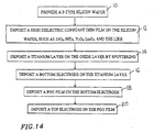
- A method of manufacturing a MFMOS one transistor memory device, comprising the steps of:providing a semiconductor substrate;depositing an oxide layer on said semiconductor substrate, said oxide layer comprising a material chosen from the group consisting of ZrO2, HfO2, Y2O3, La2O3, and mixtures thereof;depositing a bottom electrode on said oxide layer; anddepositing a PGO film on said bottom electrode.
- The method of claim 17 further comprising depositing a barrier layer between said oxide layer and said bottom electrode layer and depositing a top electrode on said PGO film, and wherein said semiconductor substrate comprises P-type Silicon, wherein said barrier layer comprises Titanium, wherein said bottom electrode comprises Iridium, and wherein said top electrode comprises Platinum.
- The method of claim 17 wherein said oxide layer comprises a material that defines a dielectric constant of at least 10.
Applications Claiming Priority (2)
| Application Number | Priority Date | Filing Date | Title |
|---|---|---|---|
| US819879 | 2001-03-27 | ||
| US09/819,879 US6503763B2 (en) | 2001-03-27 | 2001-03-27 | Method of making MFMOS capacitors with high dielectric constant materials |
Publications (2)
| Publication Number | Publication Date |
|---|---|
| EP1246253A2 true EP1246253A2 (en) | 2002-10-02 |
| EP1246253A3 EP1246253A3 (en) | 2004-10-13 |
Family
ID=25229317
Family Applications (1)
| Application Number | Title | Priority Date | Filing Date |
|---|---|---|---|
| EP02006896A Withdrawn EP1246253A3 (en) | 2001-03-27 | 2002-03-26 | MFMOS transistor memory structures with high dielectric constant materials and a method of making the same |
Country Status (5)
| Country | Link |
|---|---|
| US (2) | US6503763B2 (en) |
| EP (1) | EP1246253A3 (en) |
| JP (1) | JP2002353422A (en) |
| KR (1) | KR100479518B1 (en) |
| TW (1) | TW578269B (en) |
Families Citing this family (14)
| Publication number | Priority date | Publication date | Assignee | Title |
|---|---|---|---|---|
| US6664116B2 (en) * | 2001-12-12 | 2003-12-16 | Sharp Laboratories Of America, Inc. | Seed layer processes for MOCVD of ferroelectric thin films on high-k gate oxides |
| US7297602B2 (en) * | 2003-09-09 | 2007-11-20 | Sharp Laboratories Of America, Inc. | Conductive metal oxide gate ferroelectric memory transistor |
| US7008833B2 (en) * | 2004-01-12 | 2006-03-07 | Sharp Laboratories Of America, Inc. | In2O3thin film resistivity control by doping metal oxide insulator for MFMox device applications |
| US7267996B2 (en) * | 2004-08-20 | 2007-09-11 | Sharp Laboratories Of America, Inc. | Iridium etching for FeRAM applications |
| US7378286B2 (en) * | 2004-08-20 | 2008-05-27 | Sharp Laboratories Of America, Inc. | Semiconductive metal oxide thin film ferroelectric memory transistor |
| WO2011043794A2 (en) * | 2009-09-29 | 2011-04-14 | Yale University | Ferroelectric devices including a layer having two or more stable configurations |
| KR101605338B1 (en) * | 2014-10-02 | 2016-03-23 | 서울시립대학교 산학협력단 | Transistor with negative capacitor using topological insulator process for the preferation of the same |
| KR101623380B1 (en) * | 2014-10-02 | 2016-05-24 | 서울시립대학교 산학협력단 | Transistor with negative capacitor using feroelectric insulator and process for the preferation of the same |
| US9679893B2 (en) * | 2015-05-15 | 2017-06-13 | Taiwan Semiconductor Manufacturing Company Limited | Semiconductor device and transistor |
| JP6814915B2 (en) * | 2015-09-18 | 2021-01-20 | アドバンストマテリアルテクノロジーズ株式会社 | Ferroelectric memory and its manufacturing method, ferroelectric film and its manufacturing method |
| US10056393B2 (en) * | 2016-03-01 | 2018-08-21 | Namlab Ggmbh | Application of antiferroelectric like materials in non-volatile memory devices |
| DE102018105953B4 (en) | 2017-10-30 | 2023-09-21 | Taiwan Semiconductor Manufacturing Co. Ltd. | SEMICONDUCTOR COMPONENT AND METHOD FOR THE PRODUCTION THEREOF |
| US10784362B2 (en) * | 2017-10-30 | 2020-09-22 | Taiwan Semiconductor Manufacturing Co., Ltd. | Semiconductor device and manufacturing method thereof |
| KR102874320B1 (en) * | 2024-05-24 | 2025-10-21 | 포항공과대학교 산학협력단 | Ferroelectric transistor |
Family Cites Families (14)
| Publication number | Priority date | Publication date | Assignee | Title |
|---|---|---|---|---|
| US6559469B1 (en) * | 1992-10-23 | 2003-05-06 | Symetrix Corporation | Ferroelectric and high dielectric constant transistors |
| DE69404189T2 (en) * | 1993-03-31 | 1998-01-08 | Texas Instruments Inc | Lightly donor-doped electrodes for materials with a high dielectric constant |
| JP3250465B2 (en) * | 1996-09-06 | 2002-01-28 | ヤマハ株式会社 | How to measure electronic shading damage |
| US5731608A (en) * | 1997-03-07 | 1998-03-24 | Sharp Microelectronics Technology, Inc. | One transistor ferroelectric memory cell and method of making the same |
| US6339238B1 (en) * | 1998-10-13 | 2002-01-15 | Symetrix Corporation | Ferroelectric field effect transistor, memory utilizing same, and method of operating same |
| US6316797B1 (en) * | 1999-02-19 | 2001-11-13 | Advanced Technology Materials, Inc. | Scalable lead zirconium titanate(PZT) thin film material and deposition method, and ferroelectric memory device structures comprising such thin film material |
| US6255121B1 (en) * | 1999-02-26 | 2001-07-03 | Symetrix Corporation | Method for fabricating ferroelectric field effect transistor having an interface insulator layer formed by a liquid precursor |
| US6190925B1 (en) | 1999-04-28 | 2001-02-20 | Sharp Laboratories Of America, Inc. | Epitaxially grown lead germanate film and deposition method |
| US6236076B1 (en) * | 1999-04-29 | 2001-05-22 | Symetrix Corporation | Ferroelectric field effect transistors for nonvolatile memory applications having functional gradient material |
| US6399521B1 (en) * | 1999-05-21 | 2002-06-04 | Sharp Laboratories Of America, Inc. | Composite iridium barrier structure with oxidized refractory metal companion barrier and method for same |
| US6420740B1 (en) * | 1999-05-24 | 2002-07-16 | Sharp Laboratories Of America, Inc. | Lead germanate ferroelectric structure with multi-layered electrode |
| US6495878B1 (en) * | 1999-08-02 | 2002-12-17 | Symetrix Corporation | Interlayer oxide containing thin films for high dielectric constant application |
| US6566148B2 (en) * | 2001-08-13 | 2003-05-20 | Sharp Laboratories Of America, Inc. | Method of making a ferroelectric memory transistor |
| US6531325B1 (en) * | 2002-06-04 | 2003-03-11 | Sharp Laboratories Of America, Inc. | Memory transistor and method of fabricating same |
-
2001
- 2001-03-27 US US09/819,879 patent/US6503763B2/en not_active Expired - Fee Related
-
2002
- 2002-03-22 JP JP2002081733A patent/JP2002353422A/en active Pending
- 2002-03-26 KR KR10-2002-0016462A patent/KR100479518B1/en not_active Expired - Fee Related
- 2002-03-26 TW TW091105877A patent/TW578269B/en not_active IP Right Cessation
- 2002-03-26 EP EP02006896A patent/EP1246253A3/en not_active Withdrawn
- 2002-12-12 US US10/319,314 patent/US6716645B2/en not_active Expired - Lifetime
Also Published As
| Publication number | Publication date |
|---|---|
| US20020142487A1 (en) | 2002-10-03 |
| EP1246253A3 (en) | 2004-10-13 |
| KR100479518B1 (en) | 2005-03-30 |
| US6503763B2 (en) | 2003-01-07 |
| US20030119242A1 (en) | 2003-06-26 |
| TW578269B (en) | 2004-03-01 |
| US6716645B2 (en) | 2004-04-06 |
| JP2002353422A (en) | 2002-12-06 |
| KR20020075735A (en) | 2002-10-05 |
Similar Documents
| Publication | Publication Date | Title |
|---|---|---|
| Tokumitsu et al. | Nonvolatile ferroelectric-gate field-effect transistors using SrBi 2 Ta 2 O 9/Pt/SrTa 2 O 6/SiON/Si structures | |
| US7135736B2 (en) | Semiconductor device | |
| US6503763B2 (en) | Method of making MFMOS capacitors with high dielectric constant materials | |
| US7411237B2 (en) | Lanthanum hafnium oxide dielectrics | |
| US8815695B2 (en) | Methods to improve leakage for ZrO2 based high K MIM capacitor | |
| EP3236487B1 (en) | Method of making semiconductor ferroelectric memory element and semiconductor ferroelectric memory transistor | |
| US20020192975A1 (en) | Dielectric layer forming method and devices formed therewith | |
| KR100319571B1 (en) | Electronic Components With Doped Metal Oxide Dielectric Materials And A Process For Making Electronic Components With Doped Metal Oxide Dielectric Materials | |
| KR20010071697A (en) | Ferroelectric field effect transistor having compositionally graded ferroelectric material and method of making the same | |
| KR100562731B1 (en) | Seed layer processes for mocvd of ferroelectric thin films on high-k gate oxides | |
| US7193280B2 (en) | Indium oxide conductive film structures | |
| Kalkur et al. | Electrical characteristics of ZrO2-based metal-insulator-semiconductor structures on p-Si | |
| Li et al. | Ferroelectric Pb5Ge3O11 MFMOS capacitor for one transistor memory applications | |
| US6475813B1 (en) | MOCVD and annealing processes for C-axis oriented ferroelectric thin films | |
| KR100379245B1 (en) | Field Effect Transistor Using Zirconiumtitanate Thin Film | |
| CN113668062A (en) | Orthorhombic hafnium oxide-based ferroelectric thin film, preparation method and application thereof | |
| EP1011149A2 (en) | Semiconductor memory device and method for producing the same | |
| Gueorguiev et al. | Hysteresis in metal insulator semiconductor structures with high temperature annealed ZrO2/SiOx layers | |
| KR100363393B1 (en) | Ndro-fram memory cell device and the fabrication method there of | |
| Li et al. | The Properties of Mfmos and MFOS Capacitors with High K Gate Oxides for one Transistor Memory Applications | |
| Li et al. | Comparison of MFMOS and MFOS one transistor memory devices | |
| Li et al. | MFMOS Capacitor with Pb5Ge3O11 Thin Film for One Transistor Ferroelectric Memory Applications | |
| WO2025245088A9 (en) | Ferroelectric semiconductor devices and methods of fabricating thereof | |
| Li et al. | Selective Deposition of C-axis Oriented Pb5Ge3O11 on the Patterned High k Gate Oxide by MOCVD Processes | |
| Li et al. | Integration Processes and Properties of Pt/Pb5Ge3O11/(Zr, Hf) O2/Si One Transistor Memory Devices |
Legal Events
| Date | Code | Title | Description |
|---|---|---|---|
| PUAI | Public reference made under article 153(3) epc to a published international application that has entered the european phase |
Free format text: ORIGINAL CODE: 0009012 |
|
| AK | Designated contracting states |
Kind code of ref document: A2 Designated state(s): AT BE CH CY DE DK ES FI FR GB GR IE IT LI LU MC NL PT SE TR |
|
| AX | Request for extension of the european patent |
Free format text: AL;LT;LV;MK;RO;SI |
|
| RIN1 | Information on inventor provided before grant (corrected) |
Inventor name: MA, YANJUN Inventor name: ULRICH, BRUCE DALE Inventor name: YING, HONG Inventor name: HSU, SHENG TENG Inventor name: LI, TINGKAI |
|
| PUAL | Search report despatched |
Free format text: ORIGINAL CODE: 0009013 |
|
| AK | Designated contracting states |
Kind code of ref document: A3 Designated state(s): AT BE CH CY DE DK ES FI FR GB GR IE IT LI LU MC NL PT SE TR |
|
| AX | Request for extension of the european patent |
Extension state: AL LT LV MK RO SI |
|
| 17P | Request for examination filed |
Effective date: 20050406 |
|
| AKX | Designation fees paid |
Designated state(s): DE FR GB |
|
| STAA | Information on the status of an ep patent application or granted ep patent |
Free format text: STATUS: THE APPLICATION IS DEEMED TO BE WITHDRAWN |
|
| 18D | Application deemed to be withdrawn |
Effective date: 20080626 |