EP1245701A2 - A method of fabricating a Group III nitride film - Google Patents
A method of fabricating a Group III nitride film Download PDFInfo
- Publication number
- EP1245701A2 EP1245701A2 EP02006884A EP02006884A EP1245701A2 EP 1245701 A2 EP1245701 A2 EP 1245701A2 EP 02006884 A EP02006884 A EP 02006884A EP 02006884 A EP02006884 A EP 02006884A EP 1245701 A2 EP1245701 A2 EP 1245701A2
- Authority
- EP
- European Patent Office
- Prior art keywords
- nitride
- island
- film
- base
- nitride film
- Prior art date
- Legal status (The legal status is an assumption and is not a legal conclusion. Google has not performed a legal analysis and makes no representation as to the accuracy of the status listed.)
- Ceased
Links
Images

Classifications
-
- C—CHEMISTRY; METALLURGY
- C30—CRYSTAL GROWTH
- C30B—SINGLE-CRYSTAL GROWTH; UNIDIRECTIONAL SOLIDIFICATION OF EUTECTIC MATERIAL OR UNIDIRECTIONAL DEMIXING OF EUTECTOID MATERIAL; REFINING BY ZONE-MELTING OF MATERIAL; PRODUCTION OF A HOMOGENEOUS POLYCRYSTALLINE MATERIAL WITH DEFINED STRUCTURE; SINGLE CRYSTALS OR HOMOGENEOUS POLYCRYSTALLINE MATERIAL WITH DEFINED STRUCTURE; AFTER-TREATMENT OF SINGLE CRYSTALS OR A HOMOGENEOUS POLYCRYSTALLINE MATERIAL WITH DEFINED STRUCTURE; APPARATUS THEREFOR
- C30B29/00—Single crystals or homogeneous polycrystalline material with defined structure characterised by the material or by their shape
- C30B29/10—Inorganic compounds or compositions
- C30B29/40—AIIIBV compounds wherein A is B, Al, Ga, In or Tl and B is N, P, As, Sb or Bi
- C30B29/403—AIII-nitrides
- C30B29/406—Gallium nitride
-
- C—CHEMISTRY; METALLURGY
- C30—CRYSTAL GROWTH
- C30B—SINGLE-CRYSTAL GROWTH; UNIDIRECTIONAL SOLIDIFICATION OF EUTECTIC MATERIAL OR UNIDIRECTIONAL DEMIXING OF EUTECTOID MATERIAL; REFINING BY ZONE-MELTING OF MATERIAL; PRODUCTION OF A HOMOGENEOUS POLYCRYSTALLINE MATERIAL WITH DEFINED STRUCTURE; SINGLE CRYSTALS OR HOMOGENEOUS POLYCRYSTALLINE MATERIAL WITH DEFINED STRUCTURE; AFTER-TREATMENT OF SINGLE CRYSTALS OR A HOMOGENEOUS POLYCRYSTALLINE MATERIAL WITH DEFINED STRUCTURE; APPARATUS THEREFOR
- C30B25/00—Single-crystal growth by chemical reaction of reactive gases, e.g. chemical vapour-deposition growth
- C30B25/02—Epitaxial-layer growth
-
- C—CHEMISTRY; METALLURGY
- C30—CRYSTAL GROWTH
- C30B—SINGLE-CRYSTAL GROWTH; UNIDIRECTIONAL SOLIDIFICATION OF EUTECTIC MATERIAL OR UNIDIRECTIONAL DEMIXING OF EUTECTOID MATERIAL; REFINING BY ZONE-MELTING OF MATERIAL; PRODUCTION OF A HOMOGENEOUS POLYCRYSTALLINE MATERIAL WITH DEFINED STRUCTURE; SINGLE CRYSTALS OR HOMOGENEOUS POLYCRYSTALLINE MATERIAL WITH DEFINED STRUCTURE; AFTER-TREATMENT OF SINGLE CRYSTALS OR A HOMOGENEOUS POLYCRYSTALLINE MATERIAL WITH DEFINED STRUCTURE; APPARATUS THEREFOR
- C30B25/00—Single-crystal growth by chemical reaction of reactive gases, e.g. chemical vapour-deposition growth
- C30B25/02—Epitaxial-layer growth
- C30B25/18—Epitaxial-layer growth characterised by the substrate
-
- C—CHEMISTRY; METALLURGY
- C30—CRYSTAL GROWTH
- C30B—SINGLE-CRYSTAL GROWTH; UNIDIRECTIONAL SOLIDIFICATION OF EUTECTIC MATERIAL OR UNIDIRECTIONAL DEMIXING OF EUTECTOID MATERIAL; REFINING BY ZONE-MELTING OF MATERIAL; PRODUCTION OF A HOMOGENEOUS POLYCRYSTALLINE MATERIAL WITH DEFINED STRUCTURE; SINGLE CRYSTALS OR HOMOGENEOUS POLYCRYSTALLINE MATERIAL WITH DEFINED STRUCTURE; AFTER-TREATMENT OF SINGLE CRYSTALS OR A HOMOGENEOUS POLYCRYSTALLINE MATERIAL WITH DEFINED STRUCTURE; APPARATUS THEREFOR
- C30B29/00—Single crystals or homogeneous polycrystalline material with defined structure characterised by the material or by their shape
- C30B29/10—Inorganic compounds or compositions
- C30B29/40—AIIIBV compounds wherein A is B, Al, Ga, In or Tl and B is N, P, As, Sb or Bi
- C30B29/403—AIII-nitrides
-
- H—ELECTRICITY
- H10—SEMICONDUCTOR DEVICES; ELECTRIC SOLID-STATE DEVICES NOT OTHERWISE PROVIDED FOR
- H10P—GENERIC PROCESSES OR APPARATUS FOR THE MANUFACTURE OR TREATMENT OF DEVICES COVERED BY CLASS H10
- H10P14/00—Formation of materials, e.g. in the shape of layers or pillars
- H10P14/20—Formation of materials, e.g. in the shape of layers or pillars of semiconductor materials
- H10P14/24—Formation of materials, e.g. in the shape of layers or pillars of semiconductor materials using chemical vapour deposition [CVD]
-
- H—ELECTRICITY
- H10—SEMICONDUCTOR DEVICES; ELECTRIC SOLID-STATE DEVICES NOT OTHERWISE PROVIDED FOR
- H10P—GENERIC PROCESSES OR APPARATUS FOR THE MANUFACTURE OR TREATMENT OF DEVICES COVERED BY CLASS H10
- H10P14/00—Formation of materials, e.g. in the shape of layers or pillars
- H10P14/20—Formation of materials, e.g. in the shape of layers or pillars of semiconductor materials
- H10P14/27—Formation of materials, e.g. in the shape of layers or pillars of semiconductor materials using selective deposition, e.g. simultaneous growth of monocrystalline and non-monocrystalline semiconductor materials
- H10P14/276—Lateral overgrowth
-
- H—ELECTRICITY
- H10—SEMICONDUCTOR DEVICES; ELECTRIC SOLID-STATE DEVICES NOT OTHERWISE PROVIDED FOR
- H10P—GENERIC PROCESSES OR APPARATUS FOR THE MANUFACTURE OR TREATMENT OF DEVICES COVERED BY CLASS H10
- H10P14/00—Formation of materials, e.g. in the shape of layers or pillars
- H10P14/20—Formation of materials, e.g. in the shape of layers or pillars of semiconductor materials
- H10P14/29—Formation of materials, e.g. in the shape of layers or pillars of semiconductor materials characterised by the substrates
- H10P14/2901—Materials
-
- H—ELECTRICITY
- H10—SEMICONDUCTOR DEVICES; ELECTRIC SOLID-STATE DEVICES NOT OTHERWISE PROVIDED FOR
- H10P—GENERIC PROCESSES OR APPARATUS FOR THE MANUFACTURE OR TREATMENT OF DEVICES COVERED BY CLASS H10
- H10P14/00—Formation of materials, e.g. in the shape of layers or pillars
- H10P14/20—Formation of materials, e.g. in the shape of layers or pillars of semiconductor materials
- H10P14/29—Formation of materials, e.g. in the shape of layers or pillars of semiconductor materials characterised by the substrates
- H10P14/2901—Materials
- H10P14/2907—Materials being Group IIIA-VA materials
- H10P14/2908—Nitrides
-
- H—ELECTRICITY
- H10—SEMICONDUCTOR DEVICES; ELECTRIC SOLID-STATE DEVICES NOT OTHERWISE PROVIDED FOR
- H10P—GENERIC PROCESSES OR APPARATUS FOR THE MANUFACTURE OR TREATMENT OF DEVICES COVERED BY CLASS H10
- H10P14/00—Formation of materials, e.g. in the shape of layers or pillars
- H10P14/20—Formation of materials, e.g. in the shape of layers or pillars of semiconductor materials
- H10P14/29—Formation of materials, e.g. in the shape of layers or pillars of semiconductor materials characterised by the substrates
- H10P14/2901—Materials
- H10P14/2921—Materials being crystalline insulating materials
-
- H—ELECTRICITY
- H10—SEMICONDUCTOR DEVICES; ELECTRIC SOLID-STATE DEVICES NOT OTHERWISE PROVIDED FOR
- H10P—GENERIC PROCESSES OR APPARATUS FOR THE MANUFACTURE OR TREATMENT OF DEVICES COVERED BY CLASS H10
- H10P14/00—Formation of materials, e.g. in the shape of layers or pillars
- H10P14/20—Formation of materials, e.g. in the shape of layers or pillars of semiconductor materials
- H10P14/32—Formation of materials, e.g. in the shape of layers or pillars of semiconductor materials characterised by intermediate layers between substrates and deposited layers
- H10P14/3202—Materials thereof
- H10P14/3214—Materials thereof being Group IIIA-VA semiconductors
- H10P14/3216—Nitrides
-
- H—ELECTRICITY
- H10—SEMICONDUCTOR DEVICES; ELECTRIC SOLID-STATE DEVICES NOT OTHERWISE PROVIDED FOR
- H10P—GENERIC PROCESSES OR APPARATUS FOR THE MANUFACTURE OR TREATMENT OF DEVICES COVERED BY CLASS H10
- H10P14/00—Formation of materials, e.g. in the shape of layers or pillars
- H10P14/20—Formation of materials, e.g. in the shape of layers or pillars of semiconductor materials
- H10P14/32—Formation of materials, e.g. in the shape of layers or pillars of semiconductor materials characterised by intermediate layers between substrates and deposited layers
- H10P14/3242—Structure
-
- H—ELECTRICITY
- H10—SEMICONDUCTOR DEVICES; ELECTRIC SOLID-STATE DEVICES NOT OTHERWISE PROVIDED FOR
- H10P—GENERIC PROCESSES OR APPARATUS FOR THE MANUFACTURE OR TREATMENT OF DEVICES COVERED BY CLASS H10
- H10P14/00—Formation of materials, e.g. in the shape of layers or pillars
- H10P14/20—Formation of materials, e.g. in the shape of layers or pillars of semiconductor materials
- H10P14/34—Deposited materials, e.g. layers
- H10P14/3402—Deposited materials, e.g. layers characterised by the chemical composition
- H10P14/3414—Deposited materials, e.g. layers characterised by the chemical composition being group IIIA-VIA materials
- H10P14/3416—Nitrides
Definitions
- This invention relates to a method for fabricating a III nitride film, particularly usable as an underfilm for a semiconductor element such as a light-emitting diode or a high velocity IC chip.
- III nitride films are employed as semiconductor films constituting a light-emitting diode, and recently, win a lot of attention as semiconductor films constituting high velocity IC chips to be used in cellular phone system.
- III nitride films are usually fabricated by MOCVD methods. Concretely, a substrate on which III nitride films are formed is set onto a susceptor installed in a given reactor, and then, heated to 1000°C or over with a heater provided in or out of the susceptor. Thereafter, raw material gases are introduced with a carrier gas into the reactor and supplied onto the substrate.
- the raw material gases are dissolved through thermochemical reaction into constituent elements, which are reacted to deposit and fabricate a desired III nitride film on the substrate.
- the lattice constant of the film is changed on a larger scale.
- the difference in lattice constant between the III nitride film and the substrate is enlarged, and thus, more misfit dislocations may be created at the boundary between the III nitride film and the substrate.
- this invention relates to a method for fabricating a III nitride film, including the steps of:
- base means a given substrate and a given underfilm which are made of the first A1 including nitride.
- the inventors had intensely studied to obtain a III nitride film with lower dislocation density through an easy fabricating process without a patterned mask made of SiO 2 .
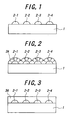
- Figs. 1-3 are conceptual views for the fabricating method of the present invention.
- island-shaped crystal portions 2-1 through 2-4 made of the second nitride, as shown in Fig. 1.
- the island-shaped crystal portions 2-1 through 2-4 are employed as nuclei for epitaxially growth.
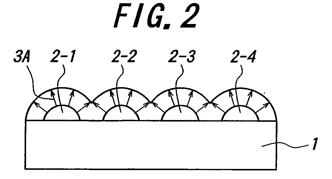
- a III nitride film 3A is epitaxially grown from the island-shaped crystal portions 2-1 through 2-4, as shown in Fig. 2, and thus, a III nitride film 3 as desired is fabricated, as shown in Fig. 3.
- the III nitride film 3A is grown three-dimensionally from the island-shaped crystal portions as nuclei in early growth step. Therefore, dislocations penetrated from the base 1 is curved and propagated laterally. As a result, even though there are many dislocations in the base 1, almost all of the dislocations are not propagated in the direction perpendicular to the surface of the base 1, that is, in the thickness direction of the III nitride film 3.
- the dislocation density of the III nitride film can be reduced. Also, since the dislocation density of the island-shaped crystal portions is very low, the dislocation density of the III nitride film can be much reduced.
- the low dislocation density of the III nitride film can be realized through the total growth process beginning with the early growth step.
- the island-shaped crystal portions can be made by controlling MOCVD condition appropriately. Three kinds of principles as follows are considered as the reason of such growth mode as follows.
- the first principle relates to the difference in lattice constant between the first A1 including nitride to form the base and the second nitride to form the island-shaped crystal portions. That is, if the lattice constant of the second nitride is larger than that of the first nitride, a given film made of the second nitride is grown on SK mode. Therefore, the film can not be formed uniformly, but grown from given nuclei in island-like shape. As a result, the above-mentioned island-shaped crystal portions are made.
- the second principle relates to the oxidation of the main surface of the base which is made of the first A1 including nitride. That is, if a given oxidized film is formed on the base through the oxidation of the main surface of the base, the second nitride is selectively deposited and agglomerated on exposed areas without the oxidized film of the main surface of the base. As a result, a uniform film can not be formed as the second nitride, and are grown three-dimensionally from the exposed areas, which is made of nitride, as nuclei. In this way, the above-mentioned island-shaped crystal portions are made.
- the third principle relates to the agglomeration due to composition fluctuation. That is, the constituents of the base is dispersed ununiformly to some degree therein, not uniformly.
- the second nitride is selectively deposited and agglomerated, correspondent with the composition distribution in the base.
- a uniform film can not be formed as the second nitride, and are grown three-dimensionally from the agglomerated portions. In this way, the above-mentioned island-shaped crystal portions are made.
- the nitride film made of the third nitride is epitaxially grown from the island-shaped crystal portions as nuclei, the nitride film is also epitaxially grown directly on the base to some degree, as shown in Fig. 2.
- the term "the nitride film made of the third nitride” means a single nitride layer and a multilayered structure made of plural nitride films such as distorted superlattice structure. Also, the term means a film of which the composition is continuously or stepwisely inclined in the thickness direction.
- This invention relates to a substrate for epitaxial growth, including;
- base also means a given substrate and a given underfilm which are made of the first A1 including nitride.
- the substrate for epitaxial growth includes the plural island-shaped crystal portions, which are made of the second nitride on the base, which is made of the first nitride. Therefore, if the substrate of the present invention is employed, a III nitride film of low dislocation density can be obtained.
- the resulting III nitride film made of the third nitride may be employed as a semiconductor film to construct a semiconductor element, particularly such as a high velocity IC chip and a semiconductor light emitting element such as light-emitting diode.
- the substrate for epitaxial growth may be employed for such a semiconductor element or a semiconductor light-emitting element. As a result, the luminance efficiency of the semiconductor light-emitting element and the high velocity response of the semiconductor element can be improved.
- plural isolated island-shaped crystal portions which are made of a second nitride, are formed on a base made of a first A1 including nitride.
- the sizes of the island-shaped crystal portions are not limited only if a nitride film made of a third nitride is epitaxially grown from the crystal portions as nuclei.
- the average area of the top surface of each island-shape crystal portion is increased.
- the average area of the top surface is set to about 100 ⁇ m 2 .
- the lower limited value of the average area of the top surface is set to 0.0001 ⁇ m 2 , particularly 1 ⁇ m 2 .
- the desired nitride film with lower dislocation density, which is made of the third nitride can be efficiently fabricated in a shorter period of time.
- the epitaxial growth condition of the nitride film is appropriately set, dependent on the sort of the first A1 including nitride to form the base, the sort of the second nitride to form the island-shaped crystal portions, the sort of the third nitride to form the nitride film as desired and the sizes of the island-shaped crystal portions.
- the first through the third nitride may be different from one another in material and composition, and two or all thereof may be equal.
- the A1 content of the second nitride is set larger than the A1 content of the first nitride.
- a given thinner film made of the second nitride is formed on the base made of the first nitride by a film growth method, such as CVD, MBE and so on, it may be affected by the compression stress from the base. Therefore, the film is grown on SK mode, and divided into plural isolated island-shaped portions.
- the island-shaped crystal portions are easily made by a normal CVD method.
- the relation of x1 ⁇ y1-0.1 is preferably satisfied for the A1 content x1 of the second nitride and the A1 content y1 of the first nitride.
- the dislocation density can be reduced up to 10 9 /cm 2 or below, particularly 10 8 /cm 2 or below.
- the above-mentioned composition relation is defined on the average compositions of the second nitride and the first nitride. Therefore, only if the composition relation is satisfied as mentioned above, particularly, the composition of the first nitride may be continuously or stepwisely inclined in the base. Moreover, the base is constructed of a distorted superlattice structure made of plural nitride films stacked periodically having their respective compositions.
- the first through the third nitrides may include an additive element such as Ge, Si, Mg, Zn, Be, P or B as occasion demands. Moreover, the first through the third nitrides may include a minute impurity contained in the raw material gases and the reactor or contained dependent on the forming condition.
- the FWHM in X-ray rocking curve at (002) reflection of the first nitride to form the base is set to 90 seconds or below, particularly 50 seconds.
- the dislocation density of the desired nitride film made of the third nitride can be much reduced.
- the surface roughness Ra of the nitride film is preferably set to 2 ⁇ or below.
- the base may be made of oxide single crystal such as sapphire single crystal, ZnO single crystal, LiAlO 2 single crystal, LiGaO 2 single crystal, MgAl 2 O 4 single crystal, or MgO single crystal, IV single crystal or IV-IV single crystal such as Si single crystal or SiC single crystal, III-V single crystal such as GaAs single crystal, AlN single crystal, GaN single crystal or AlGaN single crystal, and boride single crystal such as ZrB 2 .
- oxide single crystal such as sapphire single crystal, ZnO single crystal, LiAlO 2 single crystal, LiGaO 2 single crystal, MgAl 2 O 4 single crystal, or MgO single crystal, IV single crystal or IV-IV single crystal such as Si single crystal or SiC single crystal, III-V single crystal such as GaAs single crystal, AlN single crystal, GaN single crystal or AlGaN single crystal, and boride single crystal such as ZrB 2 .
- the base may be composed of an under base made of a single crystal as mentioned above and an epitaxial growth film made of oxide single crystal such as ZnO single crystal or MgO single crystal, IV single crystal or IV-IV single crystal such as Si single crystal or SiC single crystal, III-V single crystal such as GaAs single crystal or InP single crystal and a mixed crystal thereof.
- oxide single crystal such as ZnO single crystal or MgO single crystal
- IV single crystal or IV-IV single crystal such as Si single crystal or SiC single crystal
- III-V single crystal such as GaAs single crystal or InP single crystal and a mixed crystal thereof.
- the base is made of the sapphire single crystal or the under base is made of the sapphire single crystal and then, the epitaxial growth film is formed on the under base, it is desired that the main surface of the base or the under base is nitrided.
- the nitriding process is carried out as follows. First of all, the sapphire single crystal substrate is set in a nitrogen-including atmosphere such as an ammonia atmosphere, and then, heated for a given period. The thickness of the resulting surface nitride layer can be adjusted by controlling the nitrogen concentration, the nitriding temperature and the nitriding period appropriately.
- a nitrogen-including atmosphere such as an ammonia atmosphere
- the nitride film made of the third nitride is partially formed directly on the base, the crystal quality of the nitride film can be much enhanced if the nitride film is formed on the nitride layer of the base.
- the object of the present invention can be sufficiently realized.
- Fig. 4 is a structural view showing a semiconductor light-emitting element including a III nitride film fabricated according to the present invention.
- a semiconductor light-emitting element 10 shown in Fig. 4 includes a substrate 11, an underlayer 12 made of, for example, AIN, a first conductive layer 13 made of, for example, n-AlGaN. Then, the element 10 includes, on the first conductive layer 13, a first cladding layer 14 made of, for example, n-AlGaN which is formed on the first conductive layer 13, a light-emitting layer 15 made of, for example, i-AlGaN which is formed on the first cladding layer 14, a second cladding layer 16 made of, for example, p-AlGaN which is formed on the light-emitting layer 15, and a second conductive layer 17 made of, for example, p-AlGaN which is formed on the second cladding layer 16.
- the first conductive layer 13 is partially removed and exposed, and an n-type electrode 18 of Al/Pt is provided on the exposed surface of the first conductive layer 13. Then, a p-type electrode 19 of Au/Ni is provided on the second conductive layer 17.
- the substrate 11 is defined as the base of the present invention. Therefore, if island-shaped crystal portions are formed on the substrate 11, and then, the underlayer 12 is epitaxially grown from the island-shaped crystal portions as nuclei, the dislocation density and thus, the crystal quality of the underlayer 12 can be remarkably improved. Therefore, the crystal qualities of the first conductive layer 13 through the second conductive layer 17 can be also improved, and thus, the luminance efficiency of the semiconductor light-emitting element 10 can be enhanced.
- the substrate for epitaxial growth is composed of the substrate 11 and the island-shaped crystal portions.
- the underlayer 12 may be defined as the base of the present invention. Therefore, if island-shaped crystal portions are formed on the underlayer 12, and then, the first conductive layer 13 is epitaxially grown from the island-shaped crystal portions as nuclei, the dislocation density and thus, the crystal quality of the first conductive layer 13 can be remarkably improved. Therefore, the crystal qualities of the first cladding layer 14 through the second conductive layer 17 can be also improved, and thus, the luminance efficiency of the semiconductor light-emitting element 10 can be enhanced.
- the underlayer 12 through the second conductive layer 17 may be made by conventional MOCVD methods.
- the MOCVD condition for the layer 12 or 13 is determined on the sizes of the island-shaped crystal portions or the like.
- An under base was made of C-faced sapphire single crystal and then, set and attracted on a susceptor installed in a quartz reactor of a MOCVD apparatus, and heated to 1200°C with a heater built in or out of the susceptor. Then, an ammonia gas (NH 3 ) was flown into the reactor, and the under base was held at 1200°C under the NH 3 atmosphere for pretreatment.
- NH 3 ammonia gas
- TMA/NH 3 0.5sccm/350sccm
- TMA trimethylgallium
- TMG trimethylgallium
- the average area of the top surface of each island-shaped crystal portions was almost 1 ⁇ m 2 .
- the dislocation density of the Al 0.95 Ga 0.05 N film was turned out to be 1 ⁇ 10 9 /cm 2 by TEM observation.
- the base was held at the same temperature, and then, the TMG and the NH 3 gas were supplied onto the AlN film and the island-shaped crystal portions, to epitaxially grow a GaN film in a thickness of 3 ⁇ m.
- the dislocation density off the GaN film was turned out to be 5 ⁇ 10 7 /cm 2 by TEM observation.
- an Al 0.95 Ga 0.05 N film was made in the same manner an in Example 1.
- the dislocation density of the Al 0.95 Ga 0.05 N film was turned out to be 5 ⁇ 10 10 /cm 2 .
- Example 1 As is apparent from Examples and Comparative Example, it is turned out that the dislocation density of the Al 0.95 Ga 0.05 N film as a nitride film fabricated according to the present invention was reduced up to 10 10 /cm 2 or below, and thus, the crystal quality of the Al 0.95 Ga 0.05 N film was improved conspicuously. Moreover, compared Example 1 with Example 2, by developing the crystallinity of the AlN film as an underfilm for the Al 0.95 Ga 0.05 N film, the dislocation density of the Al 0.95 Ga 0.05 N film can be much reduced.
- the island-shaped crystal portions and the Al 0.95 Ga 0.05 N film were made in the same MOCVD apparatus, they may be made in their respective different apparatuses.
- the island-shaped crystal portions were formed directly on the base, they may be formed via a given buffer layer or a distorted superlattice structure.
- the buffer layer and the distorted superlattice structure may be made by controlling base temperature, flow rate of raw material gas, ambient pressure, amount of raw material gas or sort and amount of additive gas at MOCVD.
- a nitride film of low dislocation density and thus, high crystal quality can be easily obtained by a conventional film growth method like MOCVD, MBE and so on. Therefore, if a semiconductor element is constructed of the nitride film, the total crystal quality of the semiconductor element can be improved, and thus, the performance of the semiconductor element can be developed.
- the island-shaped crystal portions are formed on a base.
- the island-shaped crystal portions are made of a second nitride, and the base is made of a first A1 including nitride.
- a nitride film made of a third nitride is epitaxially grown from the island-shaped crystal portions as nuclei.
Landscapes
- Chemical & Material Sciences (AREA)
- Engineering & Computer Science (AREA)
- Crystallography & Structural Chemistry (AREA)
- Materials Engineering (AREA)
- Metallurgy (AREA)
- Organic Chemistry (AREA)
- Chemical Kinetics & Catalysis (AREA)
- General Chemical & Material Sciences (AREA)
- Inorganic Chemistry (AREA)
- Crystals, And After-Treatments Of Crystals (AREA)
Abstract

Description
- This invention relates to a method for fabricating a III nitride film, particularly usable as an underfilm for a semiconductor element such as a light-emitting diode or a high velocity IC chip.
- III nitride films are employed as semiconductor films constituting a light-emitting diode, and recently, win a lot of attention as semiconductor films constituting high velocity IC chips to be used in cellular phone system.
- Such III nitride films are usually fabricated by MOCVD methods. Concretely, a substrate on which III nitride films are formed is set onto a susceptor installed in a given reactor, and then, heated to 1000°C or over with a heater provided in or out of the susceptor. Thereafter, raw material gases are introduced with a carrier gas into the reactor and supplied onto the substrate.
- On the substrate, the raw material gases are dissolved through thermochemical reaction into constituent elements, which are reacted to deposit and fabricate a desired III nitride film on the substrate.
- As the composition of a III nitride film is changed, the lattice constant of the film is changed on a larger scale. In this case, the difference in lattice constant between the III nitride film and the substrate is enlarged, and thus, more misfit dislocations may be created at the boundary between the III nitride film and the substrate.
- Under the condition, if the III nitride film is epitaxially grown, many dislocations of the order of about 1010/cm2 may be created due to the propagation of the misfit dislocations. As a result, the crystal quality may be deteriorated, and thus, the electrical and optical properties of the III nitride film may be deteriorated.
- In order to eliminate the above problem, such an attention is made as making a mask of SiO2, etc., on a substrate, and epitaxially growing a III nitride film laterally on the mask. According to the epitaxially growing method, misfit dislocations, which are created at the boundary between the substrate and the III nitride film to be fabricated, are propagated only in the direction parallel to the top surface of the mask, not in the thickness direction of the III nitride film. Therefore, the dislocation density of the III nitride film can be reduced in between the pattern rods of the mask.
- In the above fabricating method, however, a lithographing process including a given etching process is required so as to fabricate the SiO2 mask, and thus, the number of step for fabricating the III nitride film is increased, causing the total fabricating process for the III nitride film to be complicated.
- It is an object of the present invention to provide a method able to easily fabricate a III nitride film of lower dislocation density, and in addition, a substrate for epitaxial growth.
- In order to achieve the above object, this invention relates to a method for fabricating a III nitride film, including the steps of:
- preparing a given base made of a first A1 including nitride,
- forming plural island-shaped crystal portions made of a second nitride which are isolated one another, and
- epitatially growing a nitride film made a third nitride from the island-shaped crystal portions as nuclei.
-
- In this invention, the term "base" means a given substrate and a given underfilm which are made of the first A1 including nitride.
- The inventors had intensely studied to obtain a III nitride film with lower dislocation density through an easy fabricating process without a patterned mask made of SiO2.
- Figs. 1-3 are conceptual views for the fabricating method of the present invention.
- First of all, on a base 1 made the first A1 including nitride are island-shaped crystal portions 2-1 through 2-4 made of the second nitride, as shown in Fig. 1. The island-shaped crystal portions 2-1 through 2-4 are employed as nuclei for epitaxially growth. Then, a III
nitride film 3A is epitaxially grown from the island-shaped crystal portions 2-1 through 2-4, as shown in Fig. 2, and thus, a III nitride film 3 as desired is fabricated, as shown in Fig. 3. - That is, since the sizes of the island-shaped crystal portions 2-1 through 2-4 are reduced remarkably, the III
nitride film 3A is grown three-dimensionally from the island-shaped crystal portions as nuclei in early growth step. Therefore, dislocations penetrated from the base 1 is curved and propagated laterally. As a result, even though there are many dislocations in the base 1, almost all of the dislocations are not propagated in the direction perpendicular to the surface of the base 1, that is, in the thickness direction of the III nitride film 3. - Accordingly, if the island-shaped crystal portions 2-1 through 2-4 are employed as nuclei for epitaxial growth and then, a III nitride film as desired is epitaxially grown from the crystal portions, the dislocation density of the III nitride film can be reduced. Also, since the dislocation density of the island-shaped crystal portions is very low, the dislocation density of the III nitride film can be much reduced.
- In the present invention, as mentioned above, since the lateral epitaxial growth is enhanced, the low dislocation density of the III nitride film can be realized through the total growth process beginning with the early growth step.
- The above-mentioned tendency becomes conspicuous, on the condition that the full width of half maximum (FWHM) of X-ray rocking curve at (002) reflection of the base 1 or an underfilm instead of the base 1 is set to 90 seconds or below.
- The island-shaped crystal portions can be made by controlling MOCVD condition appropriately. Three kinds of principles as follows are considered as the reason of such growth mode as follows.
- The first principle relates to the difference in lattice constant between the first A1 including nitride to form the base and the second nitride to form the island-shaped crystal portions. That is, if the lattice constant of the second nitride is larger than that of the first nitride, a given film made of the second nitride is grown on SK mode. Therefore, the film can not be formed uniformly, but grown from given nuclei in island-like shape. As a result, the above-mentioned island-shaped crystal portions are made.
- The second principle relates to the oxidation of the main surface of the base which is made of the first A1 including nitride. That is, if a given oxidized film is formed on the base through the oxidation of the main surface of the base, the second nitride is selectively deposited and agglomerated on exposed areas without the oxidized film of the main surface of the base. As a result, a uniform film can not be formed as the second nitride, and are grown three-dimensionally from the exposed areas, which is made of nitride, as nuclei.
In this way, the above-mentioned island-shaped crystal portions are made. - The third principle relates to the agglomeration due to composition fluctuation. That is, the constituents of the base is dispersed ununiformly to some degree therein, not uniformly. In this case, the second nitride is selectively deposited and agglomerated, correspondent with the composition distribution in the base. As a result, a uniform film can not be formed as the second nitride, and are grown three-dimensionally from the agglomerated portions. In this way, the above-mentioned island-shaped crystal portions are made.
- As mentioned above, although the nitride film made of the third nitride is epitaxially grown from the island-shaped crystal portions as nuclei, the nitride film is also epitaxially grown directly on the base to some degree, as shown in Fig. 2.
- In the present invention, the term "the nitride film made of the third nitride" means a single nitride layer and a multilayered structure made of plural nitride films such as distorted superlattice structure. Also, the term means a film of which the composition is continuously or stepwisely inclined in the thickness direction.
- This invention relates to a substrate for epitaxial growth, including;
- a base made of a first A1 including nitride, and
- plural island-shaped crystal portions made of a second nitride which are formed on the base and isolated one another.
-
- In this invention, the term "base" also means a given substrate and a given underfilm which are made of the first A1 including nitride.
- The substrate for epitaxial growth includes the plural island-shaped crystal portions, which are made of the second nitride on the base, which is made of the first nitride. Therefore, if the substrate of the present invention is employed, a III nitride film of low dislocation density can be obtained.
- The resulting III nitride film made of the third nitride may be employed as a semiconductor film to construct a semiconductor element, particularly such as a high velocity IC chip and a semiconductor light emitting element such as light-emitting diode. Also, the substrate for epitaxial growth may be employed for such a semiconductor element or a semiconductor light-emitting element. As a result, the luminance efficiency of the semiconductor light-emitting element and the high velocity response of the semiconductor element can be improved.
- For better understanding of the present invention, reference is made to the attached drawings, wherein
- Fig. 1 is a conceptual views for the fabricating method of the present invention,
- Fig. 2 is a conceptual views for the fabricating method of the present invention,
- Fig. 3 is a conceptual views for the fabricating method of the present invention, and
- Fig. 4 is a structural view showing a semiconductor light-emitting element including a III nitride film fabricated according to the present invention.
-
- This invention will be described in detail, hereinafter.
- In the present invention, it is required that plural isolated island-shaped crystal portions, which are made of a second nitride, are formed on a base made of a first A1 including nitride. The sizes of the island-shaped crystal portions are not limited only if a nitride film made of a third nitride is epitaxially grown from the crystal portions as nuclei.
- However, it is more preferable as the average area of the top surface of each island-shape crystal portion is increased. Concretely, it is desired that the average area of the top surface is set to about 100 µm2. Moreover, it is desired that the lower limited value of the average area of the top surface is set to 0.0001 µm2, particularly 1 µm2. In this case, the desired nitride film with lower dislocation density, which is made of the third nitride, can be efficiently fabricated in a shorter period of time.
- The epitaxial growth condition of the nitride film is appropriately set, dependent on the sort of the first A1 including nitride to form the base, the sort of the second nitride to form the island-shaped crystal portions, the sort of the third nitride to form the nitride film as desired and the sizes of the island-shaped crystal portions.
- The first through the third nitride may be different from one another in material and composition, and two or all thereof may be equal.
- It is also desired that the A1 content of the second nitride is set larger than the A1 content of the first nitride. In this case, if a given thinner film made of the second nitride is formed on the base made of the first nitride by a film growth method, such as CVD, MBE and so on, it may be affected by the compression stress from the base. Therefore, the film is grown on SK mode, and divided into plural isolated island-shaped portions.
- As a result, by adjusting the compositions of the first nitride and the second nitride appropriately, the island-shaped crystal portions are easily made by a normal CVD method.
- Concretely, on the condition that the composition of the second nitride is set to Alx1Gax2Inx3N (x1+x2+x3=1, x1, x2, x3≥0) and the composition of the first nitride is set to Aly1Gay2Iny3N (y1+y2+y3=1, y1>0, y2, y3≥0), the relation of x1≤y1-0.1 is preferably satisfied for the A1 content x1 of the second nitride and the A1 content y1 of the first nitride. Thereby, the dislocation density of the nitride film as desired can be easily reduced up to 1010/cm2 or below.
- Moreover, if the relation of x1≤y1-0.5 is satisfied, the dislocation density can be reduced up to 109/cm2 or below, particularly 108/cm2 or below.
- Herein, the above-mentioned composition relation is defined on the average compositions of the second nitride and the first nitride. Therefore, only if the composition relation is satisfied as mentioned above, particularly, the composition of the first nitride may be continuously or stepwisely inclined in the base. Moreover, the base is constructed of a distorted superlattice structure made of plural nitride films stacked periodically having their respective compositions.
- The first through the third nitrides may include an additive element such as Ge, Si, Mg, Zn, Be, P or B as occasion demands. Moreover, the first through the third nitrides may include a minute impurity contained in the raw material gases and the reactor or contained dependent on the forming condition.
- Moreover, it is desired that the FWHM in X-ray rocking curve at (002) reflection of the first nitride to form the base is set to 90 seconds or below, particularly 50 seconds. In this case, the dislocation density of the desired nitride film made of the third nitride can be much reduced. Similarly, the surface roughness Ra of the nitride film is preferably set to 2Å or below.
- The base may be made of oxide single crystal such as sapphire single crystal, ZnO single crystal, LiAlO2 single crystal, LiGaO2 single crystal, MgAl2O4 single crystal, or MgO single crystal, IV single crystal or IV-IV single crystal such as Si single crystal or SiC single crystal, III-V single crystal such as GaAs single crystal, AlN single crystal, GaN single crystal or AlGaN single crystal, and boride single crystal such as ZrB2.
- Moreover, the base may be composed of an under base made of a single crystal as mentioned above and an epitaxial growth film made of oxide single crystal such as ZnO single crystal or MgO single crystal, IV single crystal or IV-IV single crystal such as Si single crystal or SiC single crystal, III-V single crystal such as GaAs single crystal or InP single crystal and a mixed crystal thereof.
- Particularly, in the case that the sapphire single crystal is employed, that is, the base is made of the sapphire single crystal or the under base is made of the sapphire single crystal and then, the epitaxial growth film is formed on the under base, it is desired that the main surface of the base or the under base is nitrided.
- The nitriding process is carried out as follows. First of all, the sapphire single crystal substrate is set in a nitrogen-including atmosphere such as an ammonia atmosphere, and then, heated for a given period. The thickness of the resulting surface nitride layer can be adjusted by controlling the nitrogen concentration, the nitriding temperature and the nitriding period appropriately.
- As mentioned above, since the nitride film made of the third nitride is partially formed directly on the base, the crystal quality of the nitride film can be much enhanced if the nitride film is formed on the nitride layer of the base. However, without the nitriding process, the object of the present invention can be sufficiently realized.
- Fig. 4 is a structural view showing a semiconductor light-emitting element including a III nitride film fabricated according to the present invention.
- A semiconductor light-emitting
element 10 shown in Fig. 4 includes asubstrate 11, anunderlayer 12 made of, for example, AIN, a firstconductive layer 13 made of, for example, n-AlGaN. Then, theelement 10 includes, on the firstconductive layer 13, afirst cladding layer 14 made of, for example, n-AlGaN which is formed on the firstconductive layer 13, a light-emitting layer 15 made of, for example, i-AlGaN which is formed on thefirst cladding layer 14, asecond cladding layer 16 made of, for example, p-AlGaN which is formed on the light-emitting layer 15, and a secondconductive layer 17 made of, for example, p-AlGaN which is formed on thesecond cladding layer 16. - The first
conductive layer 13 is partially removed and exposed, and an n-type electrode 18 of Al/Pt is provided on the exposed surface of the firstconductive layer 13. Then, a p-type electrode 19 of Au/Ni is provided on the secondconductive layer 17. - In this case, the
substrate 11 is defined as the base of the present invention. Therefore, if island-shaped crystal portions are formed on thesubstrate 11, and then, theunderlayer 12 is epitaxially grown from the island-shaped crystal portions as nuclei, the dislocation density and thus, the crystal quality of theunderlayer 12 can be remarkably improved. Therefore, the crystal qualities of the firstconductive layer 13 through the secondconductive layer 17 can be also improved, and thus, the luminance efficiency of the semiconductor light-emittingelement 10 can be enhanced. - In this case, the substrate for epitaxial growth is composed of the
substrate 11 and the island-shaped crystal portions. - Moreover, the
underlayer 12 may be defined as the base of the present invention. Therefore, if island-shaped crystal portions are formed on theunderlayer 12, and then, the firstconductive layer 13 is epitaxially grown from the island-shaped crystal portions as nuclei, the dislocation density and thus, the crystal quality of the firstconductive layer 13 can be remarkably improved. Therefore, the crystal qualities of thefirst cladding layer 14 through the secondconductive layer 17 can be also improved, and thus, the luminance efficiency of the semiconductor light-emittingelement 10 can be enhanced. - Herein, the
underlayer 12 through the secondconductive layer 17 may be made by conventional MOCVD methods. In the case of epitaxially growing theunderlayer 12 or the firstconductive layer 13 from the island-shaped crystal portions, the MOCVD condition for thelayer - This invention will be concretely described hereinafter, with reference to Examples.
- An under base was made of C-faced sapphire single crystal and then, set and attracted on a susceptor installed in a quartz reactor of a MOCVD apparatus, and heated to 1200°C with a heater built in or out of the susceptor. Then, an ammonia gas (NH3) was flown into the reactor, and the under base was held at 1200°C under the NH3 atmosphere for pretreatment.
- Then, a trimethyaluminum (TMA) and an NH3 gas were employed as an A1 raw material gas and a nitrogen raw material gas, respectively, and were introduced with a H2 carrier gas into the reactor at a flow ratio of TMA/NH3= 0.5sccm/350sccm and supplied onto the substrate, to form an AlN film in a thickness of 1 µm through epitaxial growth for 60 minutes. In this way, a given base, which is composed of the under base made of sapphire single crystal and the AlN film, was fabricated. The crystallinity of the AlN film was examined by X-ray analysis, and as a result, it turned out to be 50 seconds in the FWHM.
- Then, the base temperature is lowered up to 1070°C, a trimethylgallium (TMG) was additionally employed as a Ga raw material gas. Then, the TMA, the TMG and the NH3 gas were supplied onto the AlN film at a flow ratio of TMA/TMG/NH3=0.1sccm/0.9sccm/3000sccm, to form island-shaped crystal portions made of Al0.1Ga0.9N. Herein, the average area of the top surface of each island-shaped crystal portions was almost 1 µm2.
- Then, the base temperature was increased up to 1200°C, and the raw material gases were supplied onto the base at a flow ratio of TMA/TMG/NH3= 0.95sccm/0.05sccm/350sccm, to epitaxially grow an Al0.95Ga0.05N film in a thickness of 1 µm from the island-shaped crystal portions as nuclei. The dislocation density of the Al0.95Ga0.05N film was turned out to be 1 × 10⁹/cm2 by TEM observation.
- A under base was made of C-faced sapphire single crystal, pretreated and the AlN film was formed in a thickness of 1 µm, in the same manner as in Example 1. Then, the thus obtained base was heated up to 1080°C, and the TMG and the NH3 gas were supplied onto the base at a flow rate of TMG/NH3= 1sccm/3000sccm, to form island-shaped crystal portions on the AIN film of the base. In this case, the average area top surface of each of the island-shaped crystal portions was 1 µm2.
- Then, the base was held at the same temperature, and then, the TMG and the NH3 gas were supplied onto the AlN film and the island-shaped crystal portions, to epitaxially grow a GaN film in a thickness of 3 µm. The dislocation density off the GaN film was turned out to be 5×10⁷/cm2 by TEM observation.
- Except that an AlN film was epitaxially grown on the under base heated at 900°C, island-shaped crystal portions and an Al0.95Ga0.05N film were made in the same manner as in Example 1. When the crystallinity of the Al0.95Ga0.05N film was examined by X-ray analysis, the FWHM in X-ray rocking curve at (002) reflection was about 300 seconds. Also, the dislocation density of the Al0.95Ga0.05N film was turned out to be 8×10⁹/cm2 by TEM observation.
- Except that the island-shaped crystal portions were not made, an Al0.95Ga0.05N film was made in the same manner an in Example 1. The dislocation density of the Al0.95Ga0.05N film was turned out to be 5×10¹⁰/cm2.
- As is apparent from Examples and Comparative Example, it is turned out that the dislocation density of the Al0.95Ga0.05N film as a nitride film fabricated according to the present invention was reduced up to 1010/cm2 or below, and thus, the crystal quality of the Al0.95Ga0.05N film was improved conspicuously. Moreover, compared Example 1 with Example 2, by developing the crystallinity of the AlN film as an underfilm for the Al0.95Ga0.05N film, the dislocation density of the Al0.95Ga0.05N film can be much reduced.
- As a result, if a semiconductor light-emitting element is constructed of the Al0.95Ga0.05N film, the luminance efficiency thereof can be enhanced. Similarly, if a semiconductor element such as a high velocity IC chip was constructed of the Al0.95Ga0.05N film, the response performance thereof can be enhanced.
- Although the present invention was described in detail with reference to the above examples, this invention is not limited to the above disclosure and every kind of variation and modification may be made without departing from the scope of the present invention.
- For example, in the above Examples, although the island-shaped crystal portions and the Al0.95Ga0.05N film were made in the same MOCVD apparatus, they may be made in their respective different apparatuses. Moreover, in the above embodiments, although the island-shaped crystal portions were formed directly on the base, they may be formed via a given buffer layer or a distorted superlattice structure. The buffer layer and the distorted superlattice structure may be made by controlling base temperature, flow rate of raw material gas, ambient pressure, amount of raw material gas or sort and amount of additive gas at MOCVD.
- As mentioned above, according to the present invention, a nitride film of low dislocation density and thus, high crystal quality can be easily obtained by a conventional film growth method like MOCVD, MBE and so on. Therefore, if a semiconductor element is constructed of the nitride film, the total crystal quality of the semiconductor element can be improved, and thus, the performance of the semiconductor element can be developed.
- Plural island-shaped crystal portions are formed on a base. The island-shaped crystal portions are made of a second nitride, and the base is made of a first A1 including nitride. Then, a nitride film made of a third nitride is epitaxially grown from the island-shaped crystal portions as nuclei.
Claims (15)
- A method for fabricating a III nitride film, comprising the steps of:preparing a given base made of a first A1 including nitride,forming plural island-shaped crystal portions made of a second nitride which are isolated one another, andepitatially growing a nitride film made a third nitride from said island-shaped crystal portions as nuclei.
- A fabricating method as defined in claim 1, wherein the average area of the top surface of each of said island-shaped crystal portions is set within 0.0001-1000 µm2.
- A fabricating method as defined in claim 1 or 2, wherein the A1 content of said second nitride is set smaller than the A1 content of said first A1 including nitride.
- A fabricating method as defined in claim 3, wherein said second nitride has a composition of Alx1Gax2Inx3N (x1+x2+x3=1, x1, x2, x3≥0) and said first A1 including nitride has a composition of Aly1Gay2Iny3N (y1+y2+y3=1, yl>0, y2, y3≥0), and the relation of x1≤y1-0.1 is satisfied for the A1 content x1 of said second nitride and the A1 content y1 of said first nitride.
- A fabricating method as defined on claim 4, wherein the dislocation density of said nitride film made of said third nitride is 1010/cm2 or below.
- A fabricating method as defined in claim 4, wherein the relation of x1≤y1-0.5 is satisfied for the A1 content x1 of said second nitride and the A1 content y1 of said first nitride.
- A fabricating method as defined on claim 6, wherein the dislocation density of said nitride film made of said third nitride is 109/cm2 or below.
- A fabricating method as defined in any one of claims 1-7, wherein the full width of half maximum (FWHM) in X-ray rocking curve at (002) reflection of said first A1 including nitride is 90 seconds or below.
- A substrate for epitaxial growth, comprising;a base made of a first A1 including nitride, andplural island-shaped crystal portions made of a second nitride which are formed on said base and isolated one another.
- A substrate as defined in claim 9, wherein the average area of the top surface of each of said island-shaped crystal portions is set within 0.0001-1000 µm2.
- A substrate as defined in claim 9 or 10, wherein the A1 content of said second nitride is set smaller than the A1 content of said first A1 including nitride.
- A substrate as defined in claim 11, wherein said second nitride has a composition of Alx1Gax2Inx3N (x1+x2+x3=1, x1, x2, x3≥0) and said first A1 including nitride has a composition of Aly1Gay2Iny3N (y1+y2+y3=1, yl>0, y2, y3≥0), and the relation of x1≤y1-0.1 is satisfied for the A1 content x1 of said second nitride and the A1 content y1 of said first nitride.
- A substrate as defined in any one of claims 9-12, wherein the full width of half maximum (FWHM) in X-ray rocking curve at (002) reflection of said first A1 including nitride is 90 seconds or below.
- A semiconductor element comprising a nitride film fabricated by a method as defined in any one of claims 1-8.
- A semiconductor element comprising a substrate for epitaxial growth as defined in any one of claims 9-13.
Applications Claiming Priority (6)
| Application Number | Priority Date | Filing Date | Title |
|---|---|---|---|
| JP2001091837 | 2001-03-28 | ||
| JP2001091837 | 2001-03-28 | ||
| US30312701P | 2001-07-05 | 2001-07-05 | |
| US303127P | 2001-07-05 | ||
| JP2001353212 | 2001-11-19 | ||
| JP2001353212 | 2001-11-19 |
Publications (2)
| Publication Number | Publication Date |
|---|---|
| EP1245701A2 true EP1245701A2 (en) | 2002-10-02 |
| EP1245701A3 EP1245701A3 (en) | 2009-03-04 |
Family
ID=27346371
Family Applications (1)
| Application Number | Title | Priority Date | Filing Date |
|---|---|---|---|
| EP02006884A Ceased EP1245701A3 (en) | 2001-03-28 | 2002-03-26 | A method of fabricating a Group III nitride film |
Country Status (1)
| Country | Link |
|---|---|
| EP (1) | EP1245701A3 (en) |
Cited By (3)
| Publication number | Priority date | Publication date | Assignee | Title |
|---|---|---|---|---|
| CN100477303C (en) * | 2006-01-24 | 2009-04-08 | 新世纪光电股份有限公司 | Growth method of gallium nitride semiconductor |
| US7879697B2 (en) | 2006-06-05 | 2011-02-01 | Regents Of The University Of Minnesota | Growth of low dislocation density Group-III nitrides and related thin-film structures |
| TWI728713B (en) * | 2019-02-26 | 2021-05-21 | 中國商蘇州晶湛半導體有限公司 | Method for roughening the surface of light-emitting device and light-emitting device |
Family Cites Families (2)
| Publication number | Priority date | Publication date | Assignee | Title |
|---|---|---|---|---|
| JP3587081B2 (en) * | 1999-05-10 | 2004-11-10 | 豊田合成株式会社 | Method of manufacturing group III nitride semiconductor and group III nitride semiconductor light emitting device |
| JP3786544B2 (en) * | 1999-06-10 | 2006-06-14 | パイオニア株式会社 | Nitride semiconductor device manufacturing method and device manufactured by the method |
-
2002
- 2002-03-26 EP EP02006884A patent/EP1245701A3/en not_active Ceased
Non-Patent Citations (4)
| Title |
|---|
| "Stranski-Krastanov growth", 22 April 2011 (2011-04-22), Retrieved from the Internet <URL:http://en.wikipedia.org/wiki/Stranski%E2%80%93Krastanov_growth> [retrieved on 20110606] * |
| KAWAKAMI H ET AL: "Epitaxial growth of AlN film with an initial-nitriding layer on [alpha]-Al2O3 substrate", JAPANESE JOURNAL OF APPLIED PHYSICS, PART 2 (LETTERS) JAPAN, vol. 27, no. 2, February 1988 (1988-02-01), pages L161 - L163, ISSN: 0021-4922 * |
| SUETSUGU T ET AL: "ALN EPITAXIAL GROWTH ON ATOMICALLY FLAT INITIALLY NITRIDED ALPHA-AL2O3 WAFER", APPLIED SURFACE SCIENCE, ELSEVIER, AMSTERDAM, NL, vol. 117/118, 28 October 1996 (1996-10-28), pages 540 - 545, XP009049738, ISSN: 0169-4332, DOI: 10.1016/S0169-4332(97)80139-0 * |
| UCHIDA K ET AL: "Nature of nitridated layers formed on the sapphire surface and their effect on the growth of GaN", PROCEEDINGS OF INTERNATIONAL SYMPOSIUM ON BLUE LASER AND LIGHT EMITTING DIODES - 5-7 MARCH 1996 - CHIBA, JAPAN,, 5 March 1966 (1966-03-05), pages 48 - 53, XP009148222, ISBN: 4-274-90096-7 * |
Cited By (3)
| Publication number | Priority date | Publication date | Assignee | Title |
|---|---|---|---|---|
| CN100477303C (en) * | 2006-01-24 | 2009-04-08 | 新世纪光电股份有限公司 | Growth method of gallium nitride semiconductor |
| US7879697B2 (en) | 2006-06-05 | 2011-02-01 | Regents Of The University Of Minnesota | Growth of low dislocation density Group-III nitrides and related thin-film structures |
| TWI728713B (en) * | 2019-02-26 | 2021-05-21 | 中國商蘇州晶湛半導體有限公司 | Method for roughening the surface of light-emitting device and light-emitting device |
Also Published As
| Publication number | Publication date |
|---|---|
| EP1245701A3 (en) | 2009-03-04 |
Similar Documents
| Publication | Publication Date | Title |
|---|---|---|
| EP1343927B1 (en) | Gallium nitride materials and methods for forming layers thereof | |
| EP1211715B1 (en) | A method for fabricating a III-V nitride film | |
| EP1223234B1 (en) | Epitaxial base substrate and epitaxial substrate | |
| EP1267393B1 (en) | Method of forming a group iii nitride semiconductor substrate for epitaxial lateral overgrowth (elo) | |
| US6051847A (en) | Gallium nitride compound-based semiconductor light emitting device and process for producing gallium nitride compound-based semiconductor thin film | |
| US6703255B2 (en) | Method for fabricating a III nitride film | |
| US20020175389A1 (en) | Semiconductor light-detecting element | |
| JP3946976B2 (en) | Semiconductor device, epitaxial substrate, semiconductor device manufacturing method, and epitaxial substrate manufacturing method | |
| JP2003218045A (en) | Method for producing group III nitride film | |
| JP4170269B2 (en) | Method for producing group III nitride film | |
| EP1235282A2 (en) | Method for fabricating a nitride film |
Legal Events
| Date | Code | Title | Description |
|---|---|---|---|
| PUAI | Public reference made under article 153(3) epc to a published international application that has entered the european phase |
Free format text: ORIGINAL CODE: 0009012 |
|
| AK | Designated contracting states |
Kind code of ref document: A2 Designated state(s): AT BE CH CY DE DK ES FI FR GB GR IE IT LI LU MC NL PT SE TR |
|
| AX | Request for extension of the european patent |
Free format text: AL;LT;LV;MK;RO;SI |
|
| PUAL | Search report despatched |
Free format text: ORIGINAL CODE: 0009013 |
|
| AK | Designated contracting states |
Kind code of ref document: A3 Designated state(s): AT BE CH CY DE DK ES FI FR GB GR IE IT LI LU MC NL PT SE TR |
|
| AX | Request for extension of the european patent |
Extension state: AL LT LV MK RO SI |
|
| 17P | Request for examination filed |
Effective date: 20090729 |
|
| 17Q | First examination report despatched |
Effective date: 20090904 |
|
| AKX | Designation fees paid |
Designated state(s): DE FR GB |
|
| STAA | Information on the status of an ep patent application or granted ep patent |
Free format text: STATUS: THE APPLICATION HAS BEEN REFUSED |
|
| 18R | Application refused |
Effective date: 20110608 |