EP1243956A2 - Shock proof package for an optical waveguide module - Google Patents
Shock proof package for an optical waveguide module Download PDFInfo
- Publication number
- EP1243956A2 EP1243956A2 EP02251825A EP02251825A EP1243956A2 EP 1243956 A2 EP1243956 A2 EP 1243956A2 EP 02251825 A EP02251825 A EP 02251825A EP 02251825 A EP02251825 A EP 02251825A EP 1243956 A2 EP1243956 A2 EP 1243956A2
- Authority
- EP
- European Patent Office
- Prior art keywords
- optical waveguide
- optical
- circuit chip
- waveguide
- elastic member
- Prior art date
- Legal status (The legal status is an assumption and is not a legal conclusion. Google has not performed a legal analysis and makes no representation as to the accuracy of the status listed.)
- Withdrawn
Links
- 230000003287 optical effect Effects 0.000 title claims abstract description 235
- 230000035939 shock Effects 0.000 title 1
- 239000000758 substrate Substances 0.000 claims abstract description 9
- 230000002093 peripheral effect Effects 0.000 claims abstract description 5
- 229920001973 fluoroelastomer Polymers 0.000 claims description 6
- 239000013307 optical fiber Substances 0.000 description 31
- 238000010276 construction Methods 0.000 description 13
- 230000000694 effects Effects 0.000 description 9
- 230000005540 biological transmission Effects 0.000 description 5
- 239000000853 adhesive Substances 0.000 description 4
- 230000001070 adhesive effect Effects 0.000 description 4
- 229920002449 FKM Polymers 0.000 description 3
- 238000004891 communication Methods 0.000 description 3
- XUIMIQQOPSSXEZ-UHFFFAOYSA-N Silicon Chemical compound [Si] XUIMIQQOPSSXEZ-UHFFFAOYSA-N 0.000 description 2
- 239000003795 chemical substances by application Substances 0.000 description 2
- 238000000034 method Methods 0.000 description 2
- 239000003921 oil Substances 0.000 description 2
- 230000002040 relaxant effect Effects 0.000 description 2
- 229910052710 silicon Inorganic materials 0.000 description 2
- 239000010703 silicon Substances 0.000 description 2
- RYGMFSIKBFXOCR-UHFFFAOYSA-N Copper Chemical compound [Cu] RYGMFSIKBFXOCR-UHFFFAOYSA-N 0.000 description 1
- 230000008602 contraction Effects 0.000 description 1
- 229910052802 copper Inorganic materials 0.000 description 1
- 239000010949 copper Substances 0.000 description 1
- 230000001419 dependent effect Effects 0.000 description 1
- 239000006185 dispersion Substances 0.000 description 1
- 229920001971 elastomer Polymers 0.000 description 1
- 239000003822 epoxy resin Substances 0.000 description 1
- -1 for example Polymers 0.000 description 1
- 229920000647 polyepoxide Polymers 0.000 description 1
- 230000001902 propagating effect Effects 0.000 description 1
- 230000000452 restraining effect Effects 0.000 description 1
- 239000000126 substance Substances 0.000 description 1
Images


Classifications
-
- G—PHYSICS
- G02—OPTICS
- G02B—OPTICAL ELEMENTS, SYSTEMS OR APPARATUS
- G02B6/00—Light guides; Structural details of arrangements comprising light guides and other optical elements, e.g. couplings
- G02B6/10—Light guides; Structural details of arrangements comprising light guides and other optical elements, e.g. couplings of the optical waveguide type
- G02B6/12—Light guides; Structural details of arrangements comprising light guides and other optical elements, e.g. couplings of the optical waveguide type of the integrated circuit kind
- G02B6/12007—Light guides; Structural details of arrangements comprising light guides and other optical elements, e.g. couplings of the optical waveguide type of the integrated circuit kind forming wavelength selective elements, e.g. multiplexer, demultiplexer
- G02B6/12009—Light guides; Structural details of arrangements comprising light guides and other optical elements, e.g. couplings of the optical waveguide type of the integrated circuit kind forming wavelength selective elements, e.g. multiplexer, demultiplexer comprising arrayed waveguide grating [AWG] devices, i.e. with a phased array of waveguides
- G02B6/12014—Light guides; Structural details of arrangements comprising light guides and other optical elements, e.g. couplings of the optical waveguide type of the integrated circuit kind forming wavelength selective elements, e.g. multiplexer, demultiplexer comprising arrayed waveguide grating [AWG] devices, i.e. with a phased array of waveguides characterised by the wavefront splitting or combining section, e.g. grooves or optical elements in a slab waveguide
-
- G—PHYSICS
- G02—OPTICS
- G02B—OPTICAL ELEMENTS, SYSTEMS OR APPARATUS
- G02B6/00—Light guides; Structural details of arrangements comprising light guides and other optical elements, e.g. couplings
- G02B6/10—Light guides; Structural details of arrangements comprising light guides and other optical elements, e.g. couplings of the optical waveguide type
- G02B6/12—Light guides; Structural details of arrangements comprising light guides and other optical elements, e.g. couplings of the optical waveguide type of the integrated circuit kind
- G02B6/12007—Light guides; Structural details of arrangements comprising light guides and other optical elements, e.g. couplings of the optical waveguide type of the integrated circuit kind forming wavelength selective elements, e.g. multiplexer, demultiplexer
- G02B6/12009—Light guides; Structural details of arrangements comprising light guides and other optical elements, e.g. couplings of the optical waveguide type of the integrated circuit kind forming wavelength selective elements, e.g. multiplexer, demultiplexer comprising arrayed waveguide grating [AWG] devices, i.e. with a phased array of waveguides
- G02B6/12026—Light guides; Structural details of arrangements comprising light guides and other optical elements, e.g. couplings of the optical waveguide type of the integrated circuit kind forming wavelength selective elements, e.g. multiplexer, demultiplexer comprising arrayed waveguide grating [AWG] devices, i.e. with a phased array of waveguides characterised by means for reducing the temperature dependence
- G02B6/1203—Light guides; Structural details of arrangements comprising light guides and other optical elements, e.g. couplings of the optical waveguide type of the integrated circuit kind forming wavelength selective elements, e.g. multiplexer, demultiplexer comprising arrayed waveguide grating [AWG] devices, i.e. with a phased array of waveguides characterised by means for reducing the temperature dependence using mounting means, e.g. by using a combination of materials having different thermal expansion coefficients
-
- G—PHYSICS
- G02—OPTICS
- G02B—OPTICAL ELEMENTS, SYSTEMS OR APPARATUS
- G02B6/00—Light guides; Structural details of arrangements comprising light guides and other optical elements, e.g. couplings
- G02B6/24—Coupling light guides
- G02B6/36—Mechanical coupling means
Definitions
- the present invention relates to an optical waveguide module formed by storing an optical waveguide circuit chip mainly used for optical communication into a package.
- optical waveguide circuit chips each having an optical waveguide forming area formed on a substrate are used for optical communication.
- an optical waveguide circuit chip such as a splitter and a coupler is conventionally used.
- These optical waveguide circuit chips approximately have a chip size from several mm to several ten mm.
- the optical waveguide circuit chip is generally used by connecting the chip to an optical fiber.
- the optical waveguide circuit chip and the optical fiber are connected to each other by fixing the optical waveguide circuit chip and an optical fiber block by an adhesive, etc.
- the optical fiber block is formed by fixing the optical fiber to an optical fiber arranging tool.
- the optical waveguide circuit chip normally has a thickness approximately from 0.5 mm to 1 mm, and is weak in external force. As mentioned above, when the optical waveguide circuit chip and the optical fiber block are connected to each other, the strength of a connecting portion of the optical fiber block and the optical waveguide circuit chip is also weak. Therefore, the optical waveguide circuit chip and the connecting portion of the optical waveguide circuit chip and the optical fiber block are often stored to a package and are used.
- Optical wavelength division multiplexing is vigorously researched and developed as a method for greatly increasing transmission capacity in the optical communications, and its practical use is advanced.
- the optical wavelength division multiplexing for example, a plurality of lights having wavelengths different from each other are multiplexed and transmitted.
- the optical waveguide circuit chip such as an arrayed waveguide grating and an optical switch, and an optical waveguide circuit chip of a high function integral type constructed by combining the arrayed waveguide grating and the optical switch are used for the practical use of the wavelength division multiplexing.
- the optical waveguide circuit chip such as the arrayed waveguide grating, and the optical waveguide circuit chip of a high function integral type have sizes ranging approximately from 30x30 mm to 80x80 mm and larger than the size of the conventional optical waveguide circuit chip such as a splitter and a coupler.
- An optical waveguide module of the present invention comprises:
- the arrayed waveguide grating and the optical waveguide circuit chip of a high function integral type are large in mass in comparison with the conventional optical waveguide circuit chip. Therefore, the following problem exists in an optical waveguide module in which the arrayed waveguide grating and the optical waveguide circuit chip of the high function integral type are stored into a package. Namely, no optical waveguide module of this kind can resist vibrations at a conveying time and impact applied when the optical waveguide module is dropped. Therefore, there is a case in which the optical waveguide circuit chip is damaged and a connecting portion of the optical waveguide circuit chip and the optical fiber block is damaged.
- the following results were obtained when the present inventors stored the optical waveguide circuit chip of 32mm x 34mm in size into the package and made an impact resisting test.
- the connecting portion of the optical waveguide circuit chip and the optical fiber block was cracked in 200G x 1ms (8 times/direction, 3 directions of x,y,z-axis), and an optical transmission loss was increased by 0.25 dB.
- the result cannot satisfy GR-1221-CORE as an index standard as a passive optical component, which is a serious problem.
- One aspect of the present invention resides in an optical waveguide module having a high impact resisting property and a high vibration resisting property and able to restrain a crack, etc. from being caused in the optical waveguide circuit chip and the connecting portion of the optical waveguide circuit chip and the optical fiber block even when the optical waveguide module is vibrated at a conveying time and is dropped.
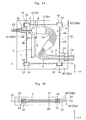
- Fig. 1A shows the main construction of a first embodiment of the optical waveguide module in the invention.
- the optical waveguide module of the first embodiment has a package having an upper cover
- Fig. 1A shows a plan view of the optical waveguide module in a state in which the package upper cover is omitted.
- Fig. 1B is a sectional view cut along a line A-A' of Fig. 1A.
- Fig. 1B is shown in a mounting state of the package upper cover.
- the optical waveguide module of the first embodiment is formed by storing an optical waveguide circuit chip 11 to a storing portion 28 within a package 30.
- the optical waveguide circuit chip 11 is supported and stored in the package 30 in at least a peripheral portion of an edge portion.
- the package 30 has a package box body 30a and a package upper cover 30b.
- the storing portion 28 of the optical waveguide circuit chip 11 is formed in the package box body 30a, and the storing portion 28 is filled with silicon oil functioning as a refractive index matching agent.
- the optical waveguide circuit chip 11 is constructed by forming an optical waveguide forming area 10 on a substrate 1, and its weight is about 10g.
- a planar shape of the optical waveguide circuit chip 11 is set to a quadrilateral shape, and the optical waveguide circuit chip 11 has 50mm in width (length in the Y-direction), and 70mm in length in the X-direction.
- the first embodiment is characterized in that an elastic member 12 for impact relaxation of the optical waveguide circuit chip 11 is arranged in the vicinity of each of three or more (here four) corner portions of the optical waveguide circuit chip 11.
- the elastic member 12 is arranged in the vicinity of each of two sets of opposite corners of the optical waveguide circuit chip 11.
- the elastic member 12 is formed in a U-like shape in section in which the optical waveguide circuit chip 11 is nipped from front and rear sides of the optical waveguide circuit chip 11.
- the elastic member 12 is formed by fluoro-elastomer,for example, viton.
- Figs. 2A to 2C show the construction of one elastic member 12 among the four elastic members 12 applied to the first embodiment.
- the constructions of the four elastic members 12 applied to the first embodiment are similar to each other.
- Fig. 2A shows a sectional view of the elastic member 12.
- Fig. 2B shows a plan view of the elastic member 12.
- Fig. 2C shows a perspective view of the elastic member 12.
- a fitting concave portion 14 for fitting the elastic member 12 thereinto is formed in the package box body 30a of the package 30.
- a clearance of about 80 ⁇ m is formed between the optical waveguide circuit chip 11 and the elastic member 12, and is also formed between the elastic member 12 and the fitting concave portion 14 of the package 30. These clearances are set to plays for moving the optical waveguide circuit chip 11 more or less within the package 30.
- the optical waveguide circuit chip 11 is an arrayed waveguide grating having a function for demultiplexing or multiplexing wavelength multiplex light having a wavelength number of 50 at an interval of 100 GHz.
- the following waveguide structure is formed in the optical waveguide forming area 10.
- the waveguide structure has at least one optical input waveguide 2, a first slab waveguide 3 connected to an output side of at least one optical input waveguide 2, an arrayed waveguide 4 connected to an output side of the first slab waveguide 3, a second slab waveguide 5 connected to an output side of the arrayed waveguide 4, and a plurality of optical output waveguides 6 connected to an output side of the second slab waveguide 5 and arranged side by side.
- the arrayed waveguide 4 includes a plurality of channel waveguides 4a for propagating light transmitted from the first slab waveguide 3 and having lengths different from each other by set amounts.
- At least one of the first slab waveguide 3 and the second slab waveguide 5 (here the first slab waveguide 3) is separated on a face (cross separating face 8) crossing a path of light passing through the first slab waveguide 3 so that separating slab waveguides 3a, 3b are formed.
- the cross separating face 8 is formed from one end side (an upper end side of Fig. 1A) of the optical waveguide forming area 10 to an intermediate portion of the optical waveguide forming area.
- a non-cross separating face 18 not crossing the first slab waveguide 3 is formed in connection with this cross separating face 8.
- the non-cross separating face 18 is arranged perpendicularly to the cross separating face 8. It is not necessary to set the non-cross separating face 18 to be perpendicular to the cross separating face 8, but Fig. 1A shows a mode in which the non-cross separating face 18 is perpendicular to the cross separating face 8.
- the optical waveguide forming area 10 is separated into a first optical waveguide forming area 10a including the separating slab waveguide 3a on one side and a second optical waveguide forming area 10b including the separating slab waveguide 3b on the other side by the cross separating face 8 and the non-cross separating face 18.
- the substrate 1 is also separated by the cross separating face 8 and the non-cross separating face 18 in accordance with the optical waveguide forming areas 10a, 10b.
- a slide moving member 7 having a coefficient of thermal expansion larger than that of the substrate 1 and the optical waveguide forming area 10 is formed in a mode crossing the first optical waveguide forming area 10a and the second optical waveguide forming area 10b. End sides of the slide moving member 7 are respectively fixed to the first optical waveguide forming area 10a and the second optical waveguide forming area 10b by a fixing portion 13.
- the slide moving member 7 slides and moves at least one side of the separating slab waveguides 3a, 3b (here the separating slab waveguide 3a) along the cross separating face 8 in accordance with the temperature of the arrayed waveguide drating.
- the slide moving member 7 slides and moves the first optical waveguide forming area 10a along the cross separating face 8 with respect to the second optical waveguide forming area 10b.
- the slide moving member 7 is arranged on surfaces of the optical waveguide forming areas 10a, 10b, and is arranged in a mode crossing the first optical waveguide forming area 10a and the second optical waveguide forming area 10b so that the following effects are obtained. Namely, the slide moving member 7 has the effect of restraining the first optical waveguide forming area 10a from being displaced in the Z-direction perpendicular to a substrate face at a slide moving time of the first optical waveguide forming area 10a.
- the slide moving member 7 is formed by a copper plate having a coefficient of thermal expansion of 1.65x10 -5 (1/K), and is formed such that the slide moving member 7 has a length able to compensate a center wavelength dependent on the temperature of the arrayed waveguide grating.
- the present inventors noticed a linear dispersion property of the arrayed waveguide grating and variously studied this property. The present inventors have then considered that the center wavelength of the arrayed waveguide grating is compensated by moving the separating slab waveguide 3a by the slide moving member 7 in accordance with temperature and shifting an output end position of the optical input waveguide 2.
- a focal center of the first slab waveguide 3 is set to a point O', and a point shifted from this point O' by a distance dx' in the X-direction is set to P'.
- P' a distance dx' in the X-direction
- an output wavelength outputted from the optical output waveguide 6 is shifted by d ⁇ ' from the output waveguide in a case in which the light is inputted from the point O'. Therefore, the output wavelength from the optical output waveguide 6 can be shifted by shifting the output end position of the optical input waveguide 2.
- L f ' shows a focal length of the first slab waveguide 3
- ⁇ L shows a difference in length between adjacent channel waveguides 4a
- n s shows an equivalent refractive index of each of the first slab waveguide 3 and the second slab waveguide 5.
- d shows a distance between adjacent channel waveguides
- n g shows a group refractive index of the arrayed waveguide.
- n g is given by the following formula 2 by using an equivalent refractive index n c of the arrayed waveguide 4 and the center wavelength ⁇ of light outputted from the optical output waveguide 6.
- the coefficient of thermal expansion and a fixing position interval (E of Fig. 1A) of the slide moving member 7 are suitably set, and the center wavelength of the arrayed waveguide grating is compensated by extending and contracting the slide moving member 7 in accordance with the temperature.
- the slide moving member 7 is constructed such that the slide moving member 7 is extended and contracted in accordance with the coefficient of thermal expansion by a length corresponding to a moving amount of the separating slab waveguide 3a according to a temperature dependence shifting amount of the center wavelength of the arrayed waveguide grating.
- the slide moving member 7 moves output ends of the separating slab waveguide 3a and the optical input waveguide 2 in the X-direction, and compensates the temperature dependence of the center wavelength of the arrayed waveguide grating.
- an optical fiber block 21 is connected to one end side of the optical waveguide circuit chip 11, and an optical fiber block 22 is connected to the other end side of the optical waveguide circuit chip 11.
- At least one optical fiber 23, 24 are respectively arranged and fixed to the optical fiber blocks 21, 22 in accordance with the optical input waveguides 2 and the optical output waveguides 6 of the arrayed waveguide grating.
- the optical fiber 23 corresponding to each optical input waveguide 2 is aligned and the optical fiber 24 corresponding to each optical output waveguide 6 is also aligned, and the optical waveguide circuit chip 11 and the optical fiber blocks 21, 22 are fixed.
- the optical fibers 23, 24 are fixed in the vicinity of a pulling-out port from the package 30 by a cemedine high super 5 (trade name) as an adhesive of an epoxy resin.
- the first embodiment is constructed as mentioned above, and this optical waveguide module is formed by arranging the elastic member 12 for impact relaxation of the optical waveguide circuit chip 11 in the vicinity of each of four corners of the vicinity of an edge portion of the optical waveguide circuit chip 11. Accordingly, even when the optical waveguide module of the first embodiment is vibrated at a conveying time and is dropped, it is possible to restrain a crack, etc. from being caused in the optical waveguide circuit chip 11 and connecting portions of the optical waveguide circuit chip 11 and the optical fiber blocks 21, 22 so that the optical waveguide module can be set to have a high impact resisting property.
- the above effects are obtained by arranging the elastic member 12 for impact relaxation of the optical waveguide circuit chip 11 in at least one portion of the vicinity of the edge portion of the optical waveguide circuit chip 11 in the construction in which the package 30 supports and stores the optical waveguide circuit chip 11 in at least a peripheral portion of the edge portion.
- the impact resisting property of the optical waveguide module can be raised if the elastic member 12 is arranged in at least one portion of the vicinity of the edge portion of the optical waveguide circuit chip 11.
- the construction of the first embodiment can further reliably show the impact resisting property improving effect.
- the impact relaxing effect of the optical waveguide circuit chip 11 can be further preferably shown.
- the elastic member 12 is formed in a U-like shape in section in which the optical waveguide circuit chip 11 is nipped from its front and rear sides. Accordingly, in the first embodiment, the impact of the optical waveguide circuit chip 11 is preferably relaxed so that a preferable impact resisting property and a preferable vibration resisting property can be set.
- the elastic member 12 is formed by fluoro-elastomer,for example, viton.
- the fluoro-elastomer is excellent in humidity resisting property and chemical resisting property, and is not easily deteriorated even when the interior of the package 30 is filled with a refractive index matching agent such as silicon oil. Therefore, the optical waveguide module of the first embodiment can be set to an optical waveguide module with high reliability able to maintain the above effects for a long period.
- the fitting concave portion 14 for fitting the elastic member 12 thereinto is arranged in the package 30 in the optical waveguide module of the first embodiment, the elastic member 12 can be more easily arranged by fitting the elastic member 12 into the fitting concave portion 12.
- a clearance for a play for moving the optical waveguide circuit chip 11 more or less within the package 30 is formed between the optical waveguide circuit chip 11 and the elastic member 12, and is also formed between the elastic member 12 and the fitting concave portion 14 of the package 30. Therefore, in the optical waveguide module of the first embodiment, the application of excessive stress to connecting portions of the optical waveguide circuit chip 11 and optical parts such as the optical fiber blocks 21, 22 can be relaxed by a play amount of this clearance so that damage of the connecting portions and an increase in transmission loss in the connecting portions can be restrained.
- the optical waveguide forming area of the optical waveguide circuit chip 11 is set to the arrayed waveguide grating, and the first slab waveguide 3 is separated into the separating slab waveguides 3a, 3b.
- the temperature dependence of the center wavelength of the arrayed waveguide grating can be reduced by moving the separating slab waveguide 3a along the cross separating face 8 by the slide moving member 7.
- the optical waveguide module of the first embodiment when applied as an optical waveguide module for wavelength division multiplexing, light at a set wavelength can be stably multiplexed and demultiplexed irrespective of the temperature so that the wavelength division multiplexing can be practically used.
- the above effect can be shown when the separating slab waveguides are formed by separating at least one of the first slab waveguide 3 and the second slab waveguide 5 on a face crossing a path of light passing through the slab waveguides, and a slide moving member for sliding and moving at least one side of the separating slab waveguides along the separating face in accordance with the temperature is arranged.
- the optical waveguide module of the second embodiment is formed approximately similarly to the first embodiment.
- the second embodiment characteristically differs from the first embodiment in that no optical waveguide circuit chip 11 is separated on the separating face in the arrayed waveguide grating as shown in Fig. 3. Further, the slide moving member 7 arranged in the first embodiment is also omitted in the second embodiment.
- the second embodiment is constructed as mentioned above. Accordingly, similar to the first embodiment, it is possible to set an optical waveguide module with high reliability having an impact resisting property and an vibration resisting property by the effect of the elastic member 12 in the second embodiment.
- the present inventors prepared the optical waveguide module of the second embodiment and an optical waveguide module having a construction approximately similar to that of this optical waveguide module and having optical fibers 23, 24 unfixed by an adhesive in a pulling-out port from the package 30. The present inventors then made an impact resisting test with respect to each of the optical waveguide modules. In the optical waveguide module in which no optical fibers 23, 24 are fixed by the adhesive in the pulling-out port from the package 30, both flexible optical fibers 23, 24 and inflexible optical fibers 23, 24 within the package 30 were prepared.
- each of the optical waveguide modules could resist 1000G x 1ms (10 times/direction, 3 directions of x,y,z-axis) in the impact resisting property irrespective of a fixing method of pulling-out portions of the optical fibers 23, 24 from the package 30.
- these optical waveguide modules satisfied GR-1221-CORE as an index standard as the above passive optical component.
- each of the optical waveguide modules could resist 20G x 10 to 2000 Hz ⁇ min/cy (6 min/cy, 6cy/axis) in the vibration resisting property.
- These optical waveguide modules also satisfied GR-1221-CORE.
- a change in optical transmission loss before and after the impact resisting test and the vibration resisting test is 0.004 dB and has no problem at all. Accordingly, reliability of these optical waveguide modules could be confirmed.
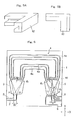
- Fig. 4 shows a sectional view of a third embodiment of the optical waveguide module in the invention.
- the same term portions as the first and second embodiments are designated by the same reference numerals, and their overlapping explanations are omitted here.
- the third embodiment is constructed approximately similarly to the second embodiment.
- the third embodiment characteristically differs from the second embodiment in the following two points.
- a first point is that a heat 40 is arranged on a lower side of the substrate 1 of the optical waveguide circuit chip 11.
- a second point is that an elastic member 12a for impact relaxation of the optical waveguide circuit chip 11 is arranged on each of upper and under sides of the optical waveguide circuit chip 11.
- the optical waveguide circuit chip 11 has 40 mm in width and 50 mm in length and the heater 40 has 28 mm in width, 35 mm in length and 100 g in weight.
- the heater 40 is set such that the temperature of the optical waveguide circuit chip 11 is held at a constant temperature such as 70 °C higher than the room temperature.
- the center wavelength of the arrayed waveguide grating is constantly held by this construction, and the third embodiment can have effects approximately similar to those in the first embodiment.
- the optical waveguide module becomes heavier in weight by arranging the heater 40. Therefore, in the third embodiment, the optical waveguide module with high reliability in the impact resisting property and the vibration resisting property is realized by arranging the elastic members 12a on the upper and under sides of the optical waveguide circuit chip 11.
- the present inventors made the impact resisting test and the vibration resisting test with respect to the third embodiment.
- the optical waveguide module of the third embodiment could resist 500G x 1ms (8 times/direction, 3 directions of x,y,z-axis) in the impact resisting property. Further, the optical waveguide module of the third embodiment could resist 20G x 10 to 2000 Hz ⁇ min/cy (6 min/cy, 6 cy/axis) in the vibration resisting property. Thus, the optical waveguide module of the third embodiment satisfied GR-1221-CORE. Further, the change in optical transmission loss before and after the impact resisting test and the vibration resisting test is 0.006 dB and has no problem at all.
- the invention is not limited to each of the above embodiments, but various embodiment modes can be adopted.
- the elastic members 12 are arranged at the four corners of the optical waveguide circuit chip 11 in each of the above embodiments, but it is sufficient to arrange the elastic member 12 in at least one portion of the vicinity of an edge portion of the optical waveguide circuit chip 11.
- the impact relaxing effect of the optical waveguide circuit chip 11 using the elastic members 12 is high when the elastic members 12 are arranged in corner portions (particularly the four corners when the optical waveguide circuit chip 11 has a quadrilateral shape) of the optical waveguide circuit chip 11.
- the elastic member 12 arranged in each of the corner portions of the optical waveguide circuit chip 11 has a shape shown in Fig. 2, but the shape of the elastic member 12 is not particularly limited, but is suitably set.
- the elastic member 12 may be also formed in shapes shown in Figs. 5A and 5B.
- the elastic members 12a are arranged on both the front and rear sides of the optical waveguide circuit chip 11, but the elastic member 12a may be also arranged on one of the front and rear sides of the optical waveguide circuit chip 11.
- the elastic members 12 and 12a are formed by fluoro-elastomer, but may be also formed by an elastic body of rubber, etc. except for the fluoro-elastomer, for example, viton.
- the clearance of about 80 ⁇ m is formed between the optical waveguide circuit chip 11 and the elastic member 12 and is also formed between the elastic member 12 and the fitting concave portion 14 of the package 30.
- this clearance is not limited to 80 ⁇ m, but may be set to range from several ⁇ m to several hundred ⁇ m. It is not necessary to form this clearance. However, it is preferable to form the clearance since the damage of connecting portions of the optical waveguide circuit chip 11 and the optical fiber blocks 21, 22 and an increase in splice loss can be restrained by forming the clearance.
- the optical waveguide circuit chip 11 is set to the arrayed waveguide grating, but the construction of the optical waveguide circuit chip 11 is not particularly limited, but is suitably set.
- the invention can be applied to an optical waveguide module in which various optical waveguide circuit chips 11 are stored and formed within the package 30.
- the optical waveguide module having a high impact resisting property and a high vibration resisting property can be realized by this application.
Landscapes
- Physics & Mathematics (AREA)
- Engineering & Computer Science (AREA)
- Microelectronics & Electronic Packaging (AREA)
- General Physics & Mathematics (AREA)
- Optics & Photonics (AREA)
- Optical Integrated Circuits (AREA)
- Optical Couplings Of Light Guides (AREA)
Abstract
Description
Claims (10)
- An optical waveguide module comprising:wherein an elastic member for impact relaxation of said optical waveguide circuit chip is arranged in at least one portion of the vicinity of the edge portion of said optical waveguide circuit chip.an optical waveguide circuit chip having an optical waveguide forming area formed on a substrate; anda package for supporting and storing the optical waveguide circuit chip in at least a peripheral portion of an edge portion;
- An optical waveguide module according to claim 1,
wherein the elastic member is formed in a U-like shape in section in which the optical waveguide circuit chip is nipped from its front and rear sides. - An optical waveguide module according to claim 1,
wherein the elastic member is arranged in the vicinity of at least one set of opposite corners of the optical waveguide circuit chip. - An optical waveguide module according to claim 1,
wherein the optical waveguide circuit chip has a quadrilateral planar shape, and
the elastic member is arranged in the vicinity of each of three or more corner portions of said optical waveguide circuit chip. - An optical waveguide module according to claim 1,
wherein the elastic member for impact relaxation of said optical waveguide circuit chip is arranged on at least one of front and rear sides of the optical waveguide circuit chip. - An optical waveguide module according to claim 1,
wherein a fitting concave portion for fitting the elastic member thereinto is arranged in the package. - An optical waveguide module according to claim 1,
wherein a clearance is formed in at least one of a portion between the optical waveguide circuit chip and the elastic member, and a portion between the elastic member and the package. - An optical waveguide module according to claim 1,
wherein the elastic member is formed by fluoro-elastomer. - An optical waveguide module according to claim 1,
wherein the optical waveguide forming area of the optical waveguide chip has:at least one optical input waveguide;a first slab waveguide connected to an output side of the optical input waveguide;an arrayed waveguide connected to an output side of the first slab waveguide and constructed by plural channel waveguides having lengths different from each other by set amounts and arranged side by side;a second slab waveguide connected to an output side of the arrayed waveguide; andone or more optical output waveguides connected to an output side of the second slab waveguide. - An optical waveguide module according to claim 1, wherein the optical waveguide forming area of the optical waveguide circuit chip has:at least one optical input waveguide;a first slab waveguide connected to an output side of the optical input waveguide;an arrayed waveguide connected to an output side of the first slab waveguide and constructed by plural channel waveguides having lengths different from each other by set amounts and arranged side by side;a second slab waveguide connected to an output side of the arrayed waveguide; andone or more optical output waveguides connected to an output side of the second slab waveguide;
wherein separating slab waveguides are formed by separating at least one of said first and second slab waveguides on a face crossing a path of light passing through the slab waveguides; anda slide moving member for sliding and moving at least one side of the separating slab waveguide along said separating face in accordance with temperature is arranged.
Applications Claiming Priority (2)
| Application Number | Priority Date | Filing Date | Title |
|---|---|---|---|
| JP2001078606 | 2001-03-19 | ||
| JP2001078606A JP4652594B2 (en) | 2001-03-19 | 2001-03-19 | Optical module |
Publications (2)
| Publication Number | Publication Date |
|---|---|
| EP1243956A2 true EP1243956A2 (en) | 2002-09-25 |
| EP1243956A3 EP1243956A3 (en) | 2004-12-01 |
Family
ID=18935199
Family Applications (1)
| Application Number | Title | Priority Date | Filing Date |
|---|---|---|---|
| EP02251825A Withdrawn EP1243956A3 (en) | 2001-03-19 | 2002-03-14 | Shock proof package for an optical waveguide module |
Country Status (4)
| Country | Link |
|---|---|
| US (1) | US6757453B2 (en) |
| EP (1) | EP1243956A3 (en) |
| JP (1) | JP4652594B2 (en) |
| CN (1) | CN1375711A (en) |
Families Citing this family (6)
| Publication number | Priority date | Publication date | Assignee | Title |
|---|---|---|---|---|
| US7418174B2 (en) * | 2002-04-26 | 2008-08-26 | Ibiden Co., Ltd. | Optical transmission structural body, optical waveguide, optical waveguide formation method, and optical wiring connection body |
| US6937783B2 (en) * | 2002-06-07 | 2005-08-30 | Charles Chu | 2-D optical switch with lens mount |
| JP2007065562A (en) * | 2005-09-02 | 2007-03-15 | Furukawa Electric Co Ltd:The | Arrayed waveguide grating |
| US8755655B2 (en) * | 2009-09-22 | 2014-06-17 | Oracle America, Inc. | Edge-coupled optical proximity communication |
| JP5281058B2 (en) * | 2010-09-24 | 2013-09-04 | 日本電信電話株式会社 | Optical parts |
| CN102495040B (en) * | 2011-11-11 | 2014-05-07 | 厦门大学 | Raman spectrometer chip adopting arrayed waveguide grating |
Family Cites Families (13)
| Publication number | Priority date | Publication date | Assignee | Title |
|---|---|---|---|---|
| JPH02166788A (en) * | 1988-12-20 | 1990-06-27 | Fujitsu Ltd | Socket for chip component |
| JPH06258220A (en) * | 1993-03-09 | 1994-09-16 | Hajime Etani | Electrolytic chemiluminescence method |
| US5335304A (en) * | 1993-04-30 | 1994-08-02 | The United States Of America As Represented By The Secretary Of The Army | Connector distribution assembly for a fiber optic detector system |
| JPH08171029A (en) | 1994-12-20 | 1996-07-02 | Hitachi Cable Ltd | Waveguide optical device |
| JPH08271756A (en) * | 1995-04-03 | 1996-10-18 | Hitachi Cable Ltd | Waveguide optical device |
| JPH09101430A (en) * | 1995-10-04 | 1997-04-15 | Hitachi Cable Ltd | Optical module |
| IL121704A (en) * | 1996-01-26 | 2000-12-06 | Sumitomo Electric Industries | Optical waveguide module |
| JP2885693B2 (en) * | 1996-04-23 | 1999-04-26 | 静岡日本電気株式会社 | LCD holding structure for small electronic devices |
| TW355752B (en) * | 1996-09-27 | 1999-04-11 | Siemens Ag | Optical coupling-device to couple the light between two waveguide-end-face |
| US5935292A (en) * | 1997-01-08 | 1999-08-10 | 3M Innovative Properties Company | Annealing mold and retainer for making a fiber optic current sensor |
| FR2770307B1 (en) * | 1997-10-27 | 1999-11-26 | Commissariat Energie Atomique | PHASE ARRAY OR PHASAR DEVICE AND MANUFACTURING METHOD THEREOF |
| US5905824A (en) * | 1997-12-09 | 1999-05-18 | Delisle; Vincent | Temperature compensated insensitive optical multiplexor/demultiplexor |
| JP2000357811A (en) * | 1999-06-15 | 2000-12-26 | Kanegafuchi Chem Ind Co Ltd | Solar cell module |
-
2001
- 2001-03-19 JP JP2001078606A patent/JP4652594B2/en not_active Expired - Fee Related
-
2002
- 2002-03-14 EP EP02251825A patent/EP1243956A3/en not_active Withdrawn
- 2002-03-18 US US10/098,532 patent/US6757453B2/en not_active Expired - Fee Related
- 2002-03-19 CN CN02108233.2A patent/CN1375711A/en active Pending
Also Published As
| Publication number | Publication date |
|---|---|
| US20020159674A1 (en) | 2002-10-31 |
| CN1375711A (en) | 2002-10-23 |
| JP4652594B2 (en) | 2011-03-16 |
| EP1243956A3 (en) | 2004-12-01 |
| US6757453B2 (en) | 2004-06-29 |
| JP2002277652A (en) | 2002-09-25 |
Similar Documents
| Publication | Publication Date | Title |
|---|---|---|
| CA2255386C (en) | Temperature compensated insensitive optical multiplexor/demultiplexor | |
| CA2320538C (en) | Arrayed waveguide grating and method for compensating optical transmitting center wavelength of light travelling through the same | |
| US7912330B2 (en) | Packaging method of temperature insensitive arrayed waveguide grating | |
| JP4665240B2 (en) | Optical transmission equipment | |
| JP3378203B2 (en) | Optical device | |
| US4756587A (en) | Optical multi/demultiplexer | |
| US6668116B2 (en) | Arrayed waveguide grating type optical multiplexer/demultiplexer | |
| US20030091289A1 (en) | Planar lightwave circuit module and method for manufacturing the same | |
| EP1326109A2 (en) | Optical fiber block with a V- groove array | |
| US20100278483A1 (en) | Athermal awg module | |
| US20020085808A1 (en) | Arrayed waveguide grating | |
| US6668117B2 (en) | Arrayed waveguide grating optical multiplexer demultiplexer | |
| US6757453B2 (en) | Optical waveguide module | |
| US20030039441A1 (en) | Arrayed waveguide grating optical multiplexer/demultiplexer and method for manufacturing the same | |
| US6769817B2 (en) | Optical fiber module | |
| US6798952B2 (en) | Optical multiplexer/demultiplexer | |
| US6829418B2 (en) | Optical waveguide circuit device | |
| US20120195552A1 (en) | Arrayed waveguide grating type optical multiplexer and demultiplexer | |
| US20040223682A1 (en) | Hybrid optical circuits with thin film filters | |
| US20020164128A1 (en) | Optical device | |
| US6724960B1 (en) | Optical coupling device | |
| JP2003021734A (en) | Optical waveguide module | |
| US20030198470A1 (en) | WDM assembly | |
| US20030012494A1 (en) | Compact optical beam separator and method | |
| WO2025173084A1 (en) | Optical module |
Legal Events
| Date | Code | Title | Description |
|---|---|---|---|
| PUAI | Public reference made under article 153(3) epc to a published international application that has entered the european phase |
Free format text: ORIGINAL CODE: 0009012 |
|
| 17P | Request for examination filed |
Effective date: 20020404 |
|
| AK | Designated contracting states |
Kind code of ref document: A2 Designated state(s): AT BE CH CY DE DK ES FI FR GB GR IE IT LI LU MC NL PT SE TR |
|
| AX | Request for extension of the european patent |
Free format text: AL;LT;LV;MK;RO;SI |
|
| PUAL | Search report despatched |
Free format text: ORIGINAL CODE: 0009013 |
|
| AK | Designated contracting states |
Kind code of ref document: A3 Designated state(s): AT BE CH CY DE DK ES FI FR GB GR IE IT LI LU MC NL PT SE TR |
|
| AX | Request for extension of the european patent |
Extension state: AL LT LV MK RO SI |
|
| 17Q | First examination report despatched |
Effective date: 20050121 |
|
| AKX | Designation fees paid |
Designated state(s): DE GB |
|
| STAA | Information on the status of an ep patent application or granted ep patent |
Free format text: STATUS: THE APPLICATION IS DEEMED TO BE WITHDRAWN |
|
| 18D | Application deemed to be withdrawn |
Effective date: 20050601 |