EP1241896A2 - Colour image pickup device with improved colour filter array - Google Patents
Colour image pickup device with improved colour filter array Download PDFInfo
- Publication number
- EP1241896A2 EP1241896A2 EP02075737A EP02075737A EP1241896A2 EP 1241896 A2 EP1241896 A2 EP 1241896A2 EP 02075737 A EP02075737 A EP 02075737A EP 02075737 A EP02075737 A EP 02075737A EP 1241896 A2 EP1241896 A2 EP 1241896A2
- Authority
- EP
- European Patent Office
- Prior art keywords
- pixel values
- light
- color
- pixel
- photosites
- Prior art date
- Legal status (The legal status is an assumption and is not a legal conclusion. Google has not performed a legal analysis and makes no representation as to the accuracy of the status listed.)
- Granted
Links
- 230000003595 spectral effect Effects 0.000 claims abstract description 4
- 238000000034 method Methods 0.000 claims description 13
- 238000012935 Averaging Methods 0.000 claims description 3
- 238000010586 diagram Methods 0.000 description 13
- 229920006395 saturated elastomer Polymers 0.000 description 5
- 238000005070 sampling Methods 0.000 description 4
- 238000003384 imaging method Methods 0.000 description 3
- 239000003086 colorant Substances 0.000 description 1
- 238000012986 modification Methods 0.000 description 1
- 230000004048 modification Effects 0.000 description 1
- 230000003287 optical effect Effects 0.000 description 1
Images




Classifications
-
- A—HUMAN NECESSITIES
- A61—MEDICAL OR VETERINARY SCIENCE; HYGIENE
- A61B—DIAGNOSIS; SURGERY; IDENTIFICATION
- A61B1/00—Instruments for performing medical examinations of the interior of cavities or tubes of the body by visual or photographical inspection, e.g. endoscopes; Illuminating arrangements therefor
- A61B1/06—Instruments for performing medical examinations of the interior of cavities or tubes of the body by visual or photographical inspection, e.g. endoscopes; Illuminating arrangements therefor with illuminating arrangements
- A61B1/0638—Instruments for performing medical examinations of the interior of cavities or tubes of the body by visual or photographical inspection, e.g. endoscopes; Illuminating arrangements therefor with illuminating arrangements providing two or more wavelengths
-
- H—ELECTRICITY
- H04—ELECTRIC COMMUNICATION TECHNIQUE
- H04N—PICTORIAL COMMUNICATION, e.g. TELEVISION
- H04N23/00—Cameras or camera modules comprising electronic image sensors; Control thereof
- H04N23/80—Camera processing pipelines; Components thereof
- H04N23/84—Camera processing pipelines; Components thereof for processing colour signals
- H04N23/843—Demosaicing, e.g. interpolating colour pixel values
-
- H—ELECTRICITY
- H04—ELECTRIC COMMUNICATION TECHNIQUE
- H04N—PICTORIAL COMMUNICATION, e.g. TELEVISION
- H04N25/00—Circuitry of solid-state image sensors [SSIS]; Control thereof
- H04N25/10—Circuitry of solid-state image sensors [SSIS]; Control thereof for transforming different wavelengths into image signals
- H04N25/11—Arrangement of colour filter arrays [CFA]; Filter mosaics
- H04N25/13—Arrangement of colour filter arrays [CFA]; Filter mosaics characterised by the spectral characteristics of the filter elements
- H04N25/133—Arrangement of colour filter arrays [CFA]; Filter mosaics characterised by the spectral characteristics of the filter elements including elements passing panchromatic light, e.g. filters passing white light
-
- H—ELECTRICITY
- H04—ELECTRIC COMMUNICATION TECHNIQUE
- H04N—PICTORIAL COMMUNICATION, e.g. TELEVISION
- H04N25/00—Circuitry of solid-state image sensors [SSIS]; Control thereof
- H04N25/10—Circuitry of solid-state image sensors [SSIS]; Control thereof for transforming different wavelengths into image signals
- H04N25/11—Arrangement of colour filter arrays [CFA]; Filter mosaics
- H04N25/13—Arrangement of colour filter arrays [CFA]; Filter mosaics characterised by the spectral characteristics of the filter elements
- H04N25/134—Arrangement of colour filter arrays [CFA]; Filter mosaics characterised by the spectral characteristics of the filter elements based on three different wavelength filter elements
Definitions
- the invention relates generally to the field of image capture, and more specifically to an image sensing device with different color types of photosites.
- Electronic image sensing devices have employed a technique of sparsely sampling photographic images with an arrangement of photosites having different color responses to light.
- sparsely sampling refers to the fact that all colors are not sensed at all photosites in the image sensing device.
- Bayer disclosed a sparsely sampled image sensing device in the form of a color filter array of photosites in US Patent 3,971,065 issued July 20, 1976 to Bayer.
- the image sensing device described by Bayer was configured in a rectangular array of photosites with luminance sensitive photosites occurring every other photosite of every row of photosite with the pattern of luminance sensitive photosites staggered by one pixel in adjacent rows of photosite.
- the luminance sensitive photosites formed a checkerboard pattern.
- the other photosites of Bayer's image sensing device used two types of chrominance, or color, sensitive photosites with a first chrominance photosite type used in the odd rows of photosites, and a second chrominance photosite type used in the even rows of photosites.
- Bayer also disclosed an alternative configuration for a sparsely sampling image sensing device in US Patent 3,971,065 that over time has proven to be more useful.
- this alternative configuration green sensitive photosites are used to sense the luminance signal and red and blue sensitive photosites are used for the two chrominance types of photosites as shown in Fig. 2a.
- the advantage of Bayer's alternative configuration is a sensor with nearly equalized photo response between the three types of photo elements, i.e. the three types of photosites saturate at nearly the same incident light level when exposed to white light.
- a disadvantage of both the Bayer configurations is evident when over exposure conditions arise. Since the green sensitive photosites have a closer relationship to the image luminance signal, many real world objects have more green image content than red or blue image content.
- the green sensitive photosites generally saturate (reach the maximum possible signal strength) faster than the red or blue sensitive photosites.
- the resulting pixel values corresponding to the saturated photosites are clipped (reach a maximum pixel value) resulting in a loss of spatial detail.
- Fig. 2b shows the Bayer pattern with X's at the locations of the saturated green photosites. These saturated green photosites may obscure image detail. Not only is there a loss of spatial detail but there is also a loss of green color information at these photosites.
- US Patent 5,323,233 issued June 21, 1994 to Yamagami et al. discloses an image sensing device color filter array of photosites with a different configuration as a variation on Bayer's pattern.
- the Yamagami pattern of photosites is shown in Fig. 3a with the Y labeled photosites responding to luminance light, and R, G, and B labeled photosites responding to red, green, and blue light respectively.
- the Yamagami pattern contains 50% luminance photosites, 25% green photosites, 121 ⁇ 2 % red photosites, and 121 ⁇ 2 % blue photosites.
- the Yamagami pattern for overexposed conditions is shown in Fig. 3b with saturated luminance photosites indicated by X's. The red, green, and blue photosites may still produce modulated signals.
- the Yamagami pattern does suffer a loss of spatial resolution due to the fact that 50% of the array are luminance response photosites.
- an image sensing device having an array of light-sensitive elements, including a first type of element sensitive to a spectral region corresponding to luminance; a second type of element sensitive primarily to red light; a third type of element sensitive primarily to green light; and a fourth type of element sensitive primarily to blue light, the four types of elements occurring in repeating patterns.
- the four types of elements of the image sensing device which occur in repeating patterns can be configured such that over at least a major portion of the array all four types of elements occur at every other element position along both of two orthogonal directions of the array of light-sensitive elements.
- An advantage of the present invention that the image sensing device minimizes the loss of spatial detail for overexposed conditions.
- Image sensing devices such as a charge-coupled device (CCD) and CMOS image sensors, are commonly found in such products as digital cameras, scanners, and video cameras.
- CCD charge-coupled device
- CMOS image sensors are commonly found in such products as digital cameras, scanners, and video cameras.
- Many image sensing devices employ an array of color filters (color filter array (CFA)), to alter the color response to light of different light sensitive elements or photosites. Thus for the geometrical locations of the photosites in a sensed image, only one characteristic response to light or color is sampled.
- CFA color filter array
- the image sensing devices which employ a color filter array are termed sparsely sampled image sensing devices.
- Digital pixel values are derived from the electronic signals produced by the photosites with electronic analog-to-digital converting circuitry.
- Pixels derived from the signal produced by a photosite type that has a primarily red color response to light are termed red pixels.
- green and blue pixels have corresponding photosite types responsive primarily to green and blue light respectively.
- Luminance pixels have corresponding photosite types responsive to red, green, and blue (white) light.
- the present invention employs a color filter array CFA pattern of light sensitive elements as shown in Fig. 1.
- the photosite locations labeled with an L are sensitive to white light and generate luminance pixel data.
- the photosite locations labeled with R, G, and B are sensitive primarily to red, green, and blue light and correspondingly generate red, green, and blue pixel data.
- Each of the four types of photosites are arranged in a rectangular pattern of every other photosite of every other row of photosites such that over at least a major portion of the array, all four types of elements occur at every other element position along both of two orthogonal directions of the array of light-sensitive elements. Note that each of the four photosite types are represented with equal frequency, i.e. each photosite type constitutes 25% of the total of photosites.
- Fig. 4 shows the CFA pattern of photosites for a local region of the image sensing device that has driven the luminance photosites into saturation by overexposure.
- the overexposed photosites are labeled with X's. Note that the red, green, and blue photosites may still record signal variations as they may not have been saturated by overexposure.
- the present invention minimizes the loss of spatial detail for overexposed conditions by virtue of the fact that only 25% of the photosites are luminance photosites.
- Imaging devices employing electronic sensors are well known, therefore the present description will be directed in particular to elements forming part of, or cooperating more directly with, apparatus in accordance with the present invention. Elements not specifically shown or described herein may be selected from those known in the art.
- image is a two dimensional array of pixel values. An image may be a two dimensional subset of another image.
- the present invention can be implemented in whole or in part within a digital camera.
- the essential elements of the present invention are shown as a functional block diagram in Fig. 5.
- a lens 2 forming a photographic image on the image sensing device 10 such as a charged-coupled device (CCD).
- CCD charged-coupled device
- An optical low pass filter 6 placed between the lens 2 and the image sensing device 10 performs a slight blurring of the imaged light in order to reduce the occurrence of aliasing.
- An A/D converter 14 receives the voltage signal corresponding to the imaged light from the image sensing device 10 and produces an image signal corresponding to the voltage signal.
- the output of the A/D converter 14 is a sparsely sampled digital image 201 .
- a sparsely sampled digital image is defined as a digital image that was captured with an image sensing device having a single image sensor with multiple types of photosites.
- the CFA interpolator 26 receives the sparsely sampled digital image 201 from the A/D converter 14 and generates an interpolated color digital image 202 by applying a color filter array CFA interpolation filter to the sparsely sampled digital image 201 .
- the CFA interpolator 26 generates color pixel values for pixel locations for which the corresponding color was not sensed by the image sensing device 10 .
- the CFA interpolator 26 generates red pixel values for pixel locations corresponding to green photosites.
- the interpolated color digital image 202 has defined red, green, and blue pixel values for all pixel locations.
- the A/D converter 14 shown in Fig. 5 converts the voltage signal produced by the image sensing device 10 into an image signal, i.e. a stream of digital pixel values corresponding to the voltage signal produced by the photosites of the image sensing device 10. More specifically, the A/D converter 14 converts the voltage signal, nearly linear with respect to the intensity of the incident light, from the image sensing device 10 to a discrete digital image signal, e.g. a 10 bit signal where the linear encoded values range from 0 to 1023.
- the A/D converter 14 may also perform processing to convert the linear code value domain image signal to a nonlinear code value domain image signal, such as an 8 bit logarithmic signal as is commonly performed in the art.
- the CFA interpolator 26 operates by considering the pixel values of the corresponding photosite and the pixel values of associated surrounding photosites. While a variety of known CFA interpolation filters may be used, the present invention uses a modified version of the CFA interpolation filter disclosed by Adams et al. in US Patent 5,652,621 issued July 29, 1997.
- the CFA interpolator 26 produces the interpolated color digital image 202 from the sparsely sampled digital image 201 in a three step procedure. In the first interpolation step, a first interpolated pixel value for all four types of pixels is generated.
- the present invention uses the first interpolated pixel values in a second interpolation step to generate color difference pixel values.
- the color difference pixel values and the first interpolated luminance pixel values are used to generate second, or final, interpolation pixel values for improved results.
- a first interpolation pixel value or missing color pixel value i.e. a color pixel value not generated directly by a photosite sensing the corresponding color of light, is generated by considering neighboring pixel values.
- This interpolation step is performed for each missing pixel value at each pixel location. Therefore, first interpolated red R', green G', and blue B' pixel values are generated at pixel locations corresponding to the luminance photosites. Similarly, first interpolated luminance L', green G', and blue B' pixel values are generated at pixel locations corresponding to the red photosites. First interpolated luminance L', red R', and blue B' pixel values are generated at pixel locations corresponding to the green photosites. First interpolated luminance L', red R', and green G' pixel values are generated at pixel locations corresponding to the blue photosites.
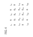
- Fig. 6 shows the pattern of pixels for generating first interpolating pixel values for red R', green G' and blue B' pixels at a pixel location corresponding to a luminance photosite.
- the first interpolated red pixel value R' 13 corresponding to the pixel location at L 13 is calculated in two terms.
- the first term is an average of two nearest neighboring red pixel values R 12 and R 14 .
- the second term is a Laplacian pixel value given by subtracting the average of the two nearest neighboring luminance pixel values L 11 and L 15 from the center luminance pixel value L 13 that are in a line, in this case a horizontal line, as the nearest neighboring red pixels.
- the first interpolated blue pixel value B' 13 corresponding to the pixel location L 13 is calculated in similar fashion with the luminance and blue pixel values sampled in the vertical direction about the center luminance pixel L 13 .
- the green photosites do not line up in either a horizontal or vertical line about the luminance photosites. However, the green photosites do lineup with the luminance photosites along the two diagonal directions.
- One of the diagonal sets of pixels is used to calculate the first interpolated green pixel value based on the magnitude of the gradients along the two diagonal directions. Specifically, the absolute value of the difference between pixels G 7 an G 19 (gradient pixel value) is compared with the absolute value of the difference between pixels G 9 an G 17 (gradient pixel value) shown in Fig. 6.
- pixels L 1 , L 13 , L 25 , G 7 , and G 19 are used in to calculate the green first interpolated pixel value G 13 corresponding to the pixel location L 13 . Otherwise, pixels L 5 , L 13 , L 21 , G 9 , and G 17 are used in to calculate the first interpolated green pixel value G' 13 corresponding to the pixel location L 13 .
- Equation (1) describes the mathematical formula for the first interpolated red, green, and blue pixel values R' 13 , G' 13 , and B' 13 respectively corresponding to the pixel location L 13
- R' 13 (R 12 + R 14 )/2 + (-L 11 - 2 L 13 -L 15 )/4
- B' 13 (B 8 + B 18 )/2 + (-L 3 - 2L 13 - L 23 )/4
- G' 13 (G 7 + G 19 )/2 + (-L 1 - 2 L 13 - L 25 )/4 for
- G' 13 (G 9 + G 17 )/2 + (-L 5 - 2L 13 - L 21 )/4 for
- ⁇
- Fig. 7 shows the pattern of pixels used for interpolating the first interpolated luminance L' 13 , green G' 13 , and blue B' 13 pixel values corresponding to the pixel location R 13 .
- the red and green pixels line up along the vertical direction while the red and luminance pixels line up along the horizontal direction.
- the blue and red pixels line up along the two diagonal directions.
- Equation (2) describes the mathematical formula for the first interpolated luminance, green, and blue pixel values L' 13 , G' 13 , and B' 13 respectively, corresponding to the pixel location R 13 .
- Fig. 8 shows the pattern of pixels used for interpolating the first interpolated luminance L' 13 , green G' 13 , and red R' 13 pixel values corresponding to the pixel location B 13 .
- the luminance and blue pixels line up along the vertical direction while the green and blue pixels line up along the horizontal direction.
- the blue and red pixels line up along the two diagonal directions.
- Equation (3) describes the mathematical formula for the first interpolated red, green, and luminance pixel values R' 13 , G' 13 , and L' 13 respectively corresponding to the pixel location B 13 .
- G' 13 (G 12 + G 14 )/2 + (-B 11 - 2 B 13 - B 15 )/4
- L' 13 (L 8 + L 18 )/2 + (-B 3 - 2B 13 -B 23 )/4
- R' 13 (R 7 + R 19 )/2 + (-B 1 - 2B 13 - B 25 )/4 for
- R' 13 (R 9 + R 17 )/2 + (-B 5 - 2B 13 -B 21 )/4 for
- ⁇
- Fig. 9 shows the pattern of pixels used for interpolating the first interpolated luminance L' 13 , red R' 13 , and blue B' 13 pixel values corresponding to the pixel location G 13 .
- the red and green pixels line up along the vertical direction while the green and blue pixels line up along the horizontal direction.
- the green and luminance pixels line up along the two diagonal directions.
- Equation (4) describes the mathematical formula for the first interpolated red, blue, and luminance pixel values R' 13 , B' 13 , and L' 13 respectively corresponding to the pixel location G 13 .
- B' 13 (B 12 + B 14 )/2 + (-G 11 - 2 G 13 - G 15 )/4
- R' 13 (R 8 + R 18 )/2 + (-G 3 - 2 G 13 - G 23 ) / 4
- L' 13 (L 7 + L 19 )/2 + (-G 1 - 2 G 13 - G 25 )/4 for
- L' 13 (L 9 + L 17 )/2 + (-G5 - 2 G 13 - G 21 )/4 for
- ⁇
- GM' green-magenta pixel value
- ILL' illuminant pixel value
- Equation (5) is used to calculate a GM' and ILL' pixel value, however, when possible, the original pixel values rather than the first interpolated pixel values are used. For example, at the red photosites, the original red pixel values R and the interpolated green G' and blue B' pixel values are used in Equation (5).
- an L', GM', and ILL' pixel is defined for all pixel locations.
- the L', GM', and ILL' pixel values are used to generate the set of second interpolated red, green, and blue pixel values R", G", and B" respectively.
- the inverse transform of Equation (5) is used to generate the R", G"", and B"" pixel values given by Equation (6).
- the original L pixel values are used in Equation (6) in place of the L' variable.
- the original pixel values R, G, and B are uses as the final interpolated pixel values at the locations of the red, green, and blue photosites respectively.
- the second interpolated red pixel values R" form the red pixel values of the interpolated color digital image 202 for the luminance, green, and blue photosite pixel locations.
- the imaging sensing device 10 experiences an overexposure condition resulting from too much light received, the luminance pixel values clip to the maximum allowable pixel value as produced by the A/D converter 26 .
- the present invention remedies the overexposure condition by using a nearest neighbor interpolation method.
- the second interpolated blue pixel value B" is calculated by averaging the two adjacent vertical original blue pixel values.
- the second interpolated red pixel value R" is calculated by averaging the two adjacent horizontal original red pixel values.
- the second interpolated green pixel value G" is calculated by first comparing the magnitude of the different between the two sets of diagonal green pixel values.
- Equation (7) describes the mathematical calculation of second interpolated red R", green G", and blue B" pixel values for the clipped pixel corresponding to the pixel location X 5 shown in Fig. 10.
- R 5 " (R 4 + R 6 ) /2
- B 5 " (B 2 + B 8 )/2
- G 5 " (G 1 + G 9 )/2 for
- G 5 " (G 3 + G 7 )/2 for
- ⁇
- the first interpolated pixel values are used. For example, at pixel location G 1 , R' and B' are used as the final interpolated pixel values R" and B" respectively. Similarly, at pixel location R 1 , G' and B' are used as the second interpolated pixel values G" and B" respectively. At pixel location B 1 , G' and R' are used as the second interpolated pixel values G" and R" respectively.
Landscapes
- Engineering & Computer Science (AREA)
- Life Sciences & Earth Sciences (AREA)
- Health & Medical Sciences (AREA)
- Physics & Mathematics (AREA)
- Multimedia (AREA)
- Signal Processing (AREA)
- Surgery (AREA)
- Spectroscopy & Molecular Physics (AREA)
- Medical Informatics (AREA)
- Animal Behavior & Ethology (AREA)
- Pathology (AREA)
- Radiology & Medical Imaging (AREA)
- Nuclear Medicine, Radiotherapy & Molecular Imaging (AREA)
- Biomedical Technology (AREA)
- Heart & Thoracic Surgery (AREA)
- Biophysics (AREA)
- Optics & Photonics (AREA)
- General Health & Medical Sciences (AREA)
- Molecular Biology (AREA)
- Public Health (AREA)
- Veterinary Medicine (AREA)
- Color Television Image Signal Generators (AREA)
- Optical Filters (AREA)
- Image Input (AREA)
- Solid State Image Pick-Up Elements (AREA)
Abstract
Description
Claims (10)
- An image sensing device having an array of light-sensitive elements, comprising a first type of element sensitive to a spectral region corresponding to luminance; a second type of element sensitive primarily to red light; a third type of element sensitive primarily to green light; and a fourth type of element sensitive primarily to blue light, the four types of elements occurring in repeating patterns.
- The image sensing device claimed in claim 1, wherein the four types of elements occurring in repeating patterns are such that over at least a major portion of the array all four types of elements occur at every other element position along both of two orthogonal directions of the array of light-sensitive elements.
- A method of capturing a color digital image, comprising the steps of:a) providing an image sensing device having an array of light-sensitive elements, which array includes at least a first type of element sensitive to a spectral region corresponding to luminance; a second type of element sensitive primarily to red light; a third type of element sensitive primarily to green light; and a fourth type of element sensitive primarily to blue light, the four types of elements occurring in repeating patterns;b) employing the image sensing device to produce a sparsely sampled digital image; andc) interpolating missing color pixel values in the sparsely sampled digital image to generate the color digital image having a color pixel value of each type for each pixel.
- The method claimed in claim 3, wherein the four types of elements occurring in repeating patterns are such that over at least a major portion of the array all four types of elements occur at every other element position along both of two orthogonal directions of the array of light-sensitive elements.
- The method claimed in claim 3, wherein the image sensing device is in a camera.
- The method claimed in claim 5, wherein the interpolation step is performed in the camera.
- The method claimed in claim 3, wherein the interpolation step includes the steps of:c1) calculating a first set of interpolated pixel values for each color at each pixel location;c2) calculating color difference pixel values for each pixel location using the first set of interpolated pixel values; andc3) calculate a final set of interpolated pixel values using the color difference pixel values.
- The method claimed in claim 7, wherein the first set of interpolated pixel values are calculated by computing a Laplacian pixel value for pixels of one color and adding the Laplacian pixel value to a pixel value of a different color.
- The method claimed in claim 7, wherein the final set of interpolated pixel values are calculated for clipped pixels using a nearest neighbor averaging technique.
- The method claimed in claim 7, wherein the luminance pixel values and the color difference pixel values are used to calculate the final set of interpolated pixel values.
Applications Claiming Priority (2)
| Application Number | Priority Date | Filing Date | Title |
|---|---|---|---|
| US800875 | 1985-11-22 | ||
| US09/800,875 US6476865B1 (en) | 2001-03-07 | 2001-03-07 | Sparsely sampled image sensing device with color and luminance photosites |
Publications (3)
| Publication Number | Publication Date |
|---|---|
| EP1241896A2 true EP1241896A2 (en) | 2002-09-18 |
| EP1241896A3 EP1241896A3 (en) | 2004-12-15 |
| EP1241896B1 EP1241896B1 (en) | 2012-10-10 |
Family
ID=25179609
Family Applications (1)
| Application Number | Title | Priority Date | Filing Date |
|---|---|---|---|
| EP02075737A Expired - Lifetime EP1241896B1 (en) | 2001-03-07 | 2002-02-22 | Colour image pickup device with improved colour filter array |
Country Status (3)
| Country | Link |
|---|---|
| US (1) | US6476865B1 (en) |
| EP (1) | EP1241896B1 (en) |
| JP (1) | JP4351825B2 (en) |
Cited By (17)
| Publication number | Priority date | Publication date | Assignee | Title |
|---|---|---|---|---|
| EP1594321A3 (en) * | 2004-05-07 | 2006-01-25 | Dialog Semiconductor GmbH | Extended dynamic range in color imagers |
| WO2008063351A1 (en) * | 2006-11-10 | 2008-05-29 | Eastman Kodak Company | Noise reduction of panchromatic and color image |
| WO2008066703A3 (en) * | 2006-11-29 | 2008-09-12 | Eastman Kodak Co | Providing a desired resolution color image |
| WO2008066699A3 (en) * | 2006-11-30 | 2008-12-04 | Eastman Kodak Co | Processing images having color and panchromatic pixels |
| WO2008150021A1 (en) * | 2007-06-06 | 2008-12-11 | Kabushiki Kaisha Toshiba | Solid-state image sensing device |
| WO2009025825A1 (en) * | 2007-08-23 | 2009-02-26 | Eastman Kodak Company | Image sensor having a color filter array with panchromatic checkerboard pattern |
| US8139130B2 (en) | 2005-07-28 | 2012-03-20 | Omnivision Technologies, Inc. | Image sensor with improved light sensitivity |
| US8194296B2 (en) | 2006-05-22 | 2012-06-05 | Omnivision Technologies, Inc. | Image sensor with improved light sensitivity |
| US8224085B2 (en) | 2007-05-23 | 2012-07-17 | Omnivision Technologies, Inc. | Noise reduced color image using panchromatic image |
| WO2012102941A1 (en) * | 2011-01-24 | 2012-08-02 | Eastman Kodak Company | Camera with multiple color sensors |
| US8274715B2 (en) | 2005-07-28 | 2012-09-25 | Omnivision Technologies, Inc. | Processing color and panchromatic pixels |
| US8416339B2 (en) | 2006-10-04 | 2013-04-09 | Omni Vision Technologies, Inc. | Providing multiple video signals from single sensor |
| US8594451B2 (en) | 2007-03-30 | 2013-11-26 | Omnivision Technologies, Inc. | Edge mapping incorporating panchromatic pixels |
| EP2926718A1 (en) * | 2014-03-31 | 2015-10-07 | Fujifilm Corporation | Endoscope system and method for operating endoscope system |
| EP3547680A1 (en) * | 2018-03-28 | 2019-10-02 | Blackmagic Design Pty Ltd | Image processing method and filter array |
| US10531067B2 (en) | 2017-03-26 | 2020-01-07 | Apple Inc. | Enhancing spatial resolution in a stereo camera imaging system |
| US20210192742A1 (en) * | 2019-12-18 | 2021-06-24 | Realtek Semiconductor Corp. | Method and system for image correction |
Families Citing this family (48)
| Publication number | Priority date | Publication date | Assignee | Title |
|---|---|---|---|---|
| JP4162111B2 (en) * | 1999-07-27 | 2008-10-08 | 富士フイルム株式会社 | Image processing method and apparatus, and recording medium |
| US6900838B1 (en) * | 1999-10-14 | 2005-05-31 | Hitachi Denshi Kabushiki Kaisha | Method of processing image signal from solid-state imaging device, image signal processing apparatus, image signal generating apparatus and computer program product for image signal processing method |
| GB9925902D0 (en) * | 1999-11-03 | 1999-12-29 | Vlsi Vision Ltd | Colour image restoration with anti-alias |
| US7053908B2 (en) * | 2001-04-12 | 2006-05-30 | Polaroid Corporation | Method and apparatus for sensing and interpolating color image data |
| US7583279B2 (en) * | 2004-04-09 | 2009-09-01 | Samsung Electronics Co., Ltd. | Subpixel layouts and arrangements for high brightness displays |
| JP2006165975A (en) * | 2004-12-07 | 2006-06-22 | Konica Minolta Photo Imaging Inc | Image pickup element, image pickup device and image processing method |
| US7570290B2 (en) | 2004-12-27 | 2009-08-04 | Sony Corporation | Drive method for solid-state imaging device, solid-state imaging device, and imaging apparatus |
| US7568628B2 (en) | 2005-03-11 | 2009-08-04 | Hand Held Products, Inc. | Bar code reading device with global electronic shutter control |
| US7611060B2 (en) | 2005-03-11 | 2009-11-03 | Hand Held Products, Inc. | System and method to automatically focus an image reader |
| US7780089B2 (en) | 2005-06-03 | 2010-08-24 | Hand Held Products, Inc. | Digital picture taking optical reader having hybrid monochrome and color image sensor array |
| US7770799B2 (en) | 2005-06-03 | 2010-08-10 | Hand Held Products, Inc. | Optical reader having reduced specular reflection read failures |
| US20070046807A1 (en) * | 2005-08-23 | 2007-03-01 | Eastman Kodak Company | Capturing images under varying lighting conditions |
| JP5118047B2 (en) * | 2005-10-13 | 2013-01-16 | アール・ジェイ・エス・テクノロジー・インコーポレイテッド | System and method for high performance color filter mosaic array |
| US7821553B2 (en) * | 2005-12-30 | 2010-10-26 | International Business Machines Corporation | Pixel array, imaging sensor including the pixel array and digital camera including the imaging sensor |
| US20070159542A1 (en) * | 2006-01-12 | 2007-07-12 | Gang Luo | Color filter array with neutral elements and color image formation |
| CN101150731B (en) * | 2006-09-22 | 2012-05-23 | 罗罡 | Color filtering array for digital imaging and its imaging method |
| WO2007082289A2 (en) * | 2006-01-12 | 2007-07-19 | Gang Luo | Color filter array with neutral elements and color image formation |
| US7688368B2 (en) * | 2006-01-27 | 2010-03-30 | Eastman Kodak Company | Image sensor with improved light sensitivity |
| JP4796871B2 (en) * | 2006-03-06 | 2011-10-19 | 富士フイルム株式会社 | Imaging device |
| JP5011814B2 (en) * | 2006-05-15 | 2012-08-29 | ソニー株式会社 | Imaging apparatus, image processing method, and computer program |
| JP4616794B2 (en) * | 2006-05-18 | 2011-01-19 | 富士フイルム株式会社 | Image data noise reduction apparatus and control method therefor |
| US7769230B2 (en) * | 2006-11-30 | 2010-08-03 | Eastman Kodak Company | Producing low resolution images |
| US7893976B2 (en) * | 2006-12-01 | 2011-02-22 | Eastman Kodak Company | Light sensitivity in image sensors |
| JP5222625B2 (en) * | 2007-06-01 | 2013-06-26 | 富士フイルム株式会社 | Imaging device |
| US8045022B2 (en) * | 2007-06-12 | 2011-10-25 | Fujifilm Corporation | Imaging apparatus for correcting a luminance signal |
| JP5033711B2 (en) * | 2007-06-13 | 2012-09-26 | 富士フイルム株式会社 | Imaging device and driving method of imaging device |
| US8199230B2 (en) * | 2007-06-28 | 2012-06-12 | Fujifilm Corporation | Signal processing apparatus, image pickup apparatus and computer readable medium |
| US8896712B2 (en) * | 2007-07-20 | 2014-11-25 | Omnivision Technologies, Inc. | Determining and correcting for imaging device motion during an exposure |
| US7855740B2 (en) * | 2007-07-20 | 2010-12-21 | Eastman Kodak Company | Multiple component readout of image sensor |
| US8452082B2 (en) * | 2007-09-27 | 2013-05-28 | Eastman Kodak Company | Pattern conversion for interpolation |
| US8164651B2 (en) * | 2008-04-29 | 2012-04-24 | Omnivision Technologies, Inc. | Concentric exposure sequence for image sensor |
| US8350952B2 (en) * | 2008-06-04 | 2013-01-08 | Omnivision Technologies, Inc. | Image sensors with improved angle response |
| US7859033B2 (en) | 2008-07-09 | 2010-12-28 | Eastman Kodak Company | Wafer level processing for backside illuminated sensors |
| US7915067B2 (en) * | 2008-07-09 | 2011-03-29 | Eastman Kodak Company | Backside illuminated image sensor with reduced dark current |
| US8111307B2 (en) * | 2008-10-25 | 2012-02-07 | Omnivision Technologies, Inc. | Defective color and panchromatic CFA image |
| US8587681B2 (en) | 2008-11-21 | 2013-11-19 | Omnivision Technologies, Inc. | Extended depth of field for image sensor |
| TW201035909A (en) * | 2009-03-25 | 2010-10-01 | Altek Corp | Compensation method for removing image noise |
| US8218068B2 (en) | 2009-04-01 | 2012-07-10 | Omnivision Technologies, Inc. | Exposing pixel groups in producing digital images |
| US20110115954A1 (en) | 2009-11-19 | 2011-05-19 | Eastman Kodak Company | Sparse color pixel array with pixel substitutes |
| JP5585208B2 (en) * | 2010-05-20 | 2014-09-10 | ソニー株式会社 | Solid-state imaging device and electronic apparatus |
| US20120105584A1 (en) | 2010-10-28 | 2012-05-03 | Gallagher Andrew C | Camera with sensors having different color patterns |
| JP6196900B2 (en) * | 2013-12-18 | 2017-09-13 | オリンパス株式会社 | Endoscope device |
| CN103714751B (en) * | 2013-12-30 | 2016-06-22 | 北京京东方光电科技有限公司 | Pel array and driving method, display floater and display device |
| US9225889B1 (en) | 2014-08-18 | 2015-12-29 | Entropix, Inc. | Photographic image acquisition device and method |
| KR102547655B1 (en) | 2015-11-18 | 2023-06-23 | 삼성전자주식회사 | Image sensor and electronic device including the same |
| US9998695B2 (en) * | 2016-01-29 | 2018-06-12 | Ford Global Technologies, Llc | Automotive imaging system including an electronic image sensor having a sparse color filter array |
| US10644073B2 (en) | 2016-12-19 | 2020-05-05 | Samsung Electronics Co., Ltd. | Image sensors and electronic devices including the same |
| KR20240114118A (en) * | 2023-01-16 | 2024-07-23 | 에스케이하이닉스 주식회사 | Image processing device and image processing method |
Family Cites Families (14)
| Publication number | Priority date | Publication date | Assignee | Title |
|---|---|---|---|---|
| US3971065A (en) | 1975-03-05 | 1976-07-20 | Eastman Kodak Company | Color imaging array |
| US4630307A (en) * | 1984-09-10 | 1986-12-16 | Eastman Kodak Company | Signal processing method and apparatus for sampled image signals |
| US4724395A (en) * | 1985-08-05 | 1988-02-09 | Polaroid Corporation | Median filter for reconstructing missing color samples |
| US5323233A (en) | 1990-07-31 | 1994-06-21 | Canon Kabushiki Kaisha | Image signal processing apparatus having a color filter with offset luminance filter elements |
| US5382976A (en) * | 1993-06-30 | 1995-01-17 | Eastman Kodak Company | Apparatus and method for adaptively interpolating a full color image utilizing luminance gradients |
| JPH08186761A (en) * | 1994-12-30 | 1996-07-16 | Sony Corp | Video camera device and video camera exposure control method |
| US5629734A (en) * | 1995-03-17 | 1997-05-13 | Eastman Kodak Company | Adaptive color plan interpolation in single sensor color electronic camera |
| US5652621A (en) | 1996-02-23 | 1997-07-29 | Eastman Kodak Company | Adaptive color plane interpolation in single sensor color electronic camera |
| US5808674A (en) * | 1996-09-09 | 1998-09-15 | Eastman Kodak Company | Producing and improved digital image from digital signals corresponding to pairs of photosites |
| JP3925588B2 (en) * | 1997-11-25 | 2007-06-06 | セイコーエプソン株式会社 | Image processing apparatus, image processing method, and medium on which image processing control program is recorded |
| US5990950A (en) * | 1998-02-11 | 1999-11-23 | Iterated Systems, Inc. | Method and system for color filter array multifactor interpolation |
| US6958772B1 (en) * | 1999-01-20 | 2005-10-25 | Canon Kabushiki Kaisha | Image sensing apparatus and image processing method therefor |
| US6714243B1 (en) * | 1999-03-22 | 2004-03-30 | Biomorphic Vlsi, Inc. | Color filter pattern |
| JP4317619B2 (en) * | 1999-07-22 | 2009-08-19 | メディア・テック・ユーエスエイ・インコーポレーテッド | Image processing device |
-
2001
- 2001-03-07 US US09/800,875 patent/US6476865B1/en not_active Expired - Lifetime
-
2002
- 2002-02-22 EP EP02075737A patent/EP1241896B1/en not_active Expired - Lifetime
- 2002-03-05 JP JP2002059225A patent/JP4351825B2/en not_active Expired - Lifetime
Cited By (27)
| Publication number | Priority date | Publication date | Assignee | Title |
|---|---|---|---|---|
| EP1594321A3 (en) * | 2004-05-07 | 2006-01-25 | Dialog Semiconductor GmbH | Extended dynamic range in color imagers |
| US8330839B2 (en) | 2005-07-28 | 2012-12-11 | Omnivision Technologies, Inc. | Image sensor with improved light sensitivity |
| US8711452B2 (en) | 2005-07-28 | 2014-04-29 | Omnivision Technologies, Inc. | Processing color and panchromatic pixels |
| US8274715B2 (en) | 2005-07-28 | 2012-09-25 | Omnivision Technologies, Inc. | Processing color and panchromatic pixels |
| US8139130B2 (en) | 2005-07-28 | 2012-03-20 | Omnivision Technologies, Inc. | Image sensor with improved light sensitivity |
| US8194296B2 (en) | 2006-05-22 | 2012-06-05 | Omnivision Technologies, Inc. | Image sensor with improved light sensitivity |
| US8416339B2 (en) | 2006-10-04 | 2013-04-09 | Omni Vision Technologies, Inc. | Providing multiple video signals from single sensor |
| WO2008063351A1 (en) * | 2006-11-10 | 2008-05-29 | Eastman Kodak Company | Noise reduction of panchromatic and color image |
| US7876956B2 (en) | 2006-11-10 | 2011-01-25 | Eastman Kodak Company | Noise reduction of panchromatic and color image |
| WO2008066703A3 (en) * | 2006-11-29 | 2008-09-12 | Eastman Kodak Co | Providing a desired resolution color image |
| WO2008066699A3 (en) * | 2006-11-30 | 2008-12-04 | Eastman Kodak Co | Processing images having color and panchromatic pixels |
| US7769229B2 (en) | 2006-11-30 | 2010-08-03 | Eastman Kodak Company | Processing images having color and panchromatic pixels |
| US8594451B2 (en) | 2007-03-30 | 2013-11-26 | Omnivision Technologies, Inc. | Edge mapping incorporating panchromatic pixels |
| US8224085B2 (en) | 2007-05-23 | 2012-07-17 | Omnivision Technologies, Inc. | Noise reduced color image using panchromatic image |
| WO2008150021A1 (en) * | 2007-06-06 | 2008-12-11 | Kabushiki Kaisha Toshiba | Solid-state image sensing device |
| US8045033B2 (en) | 2007-06-06 | 2011-10-25 | Kabushiki Kaisha Toshiba | Solid-state image sensing device |
| WO2009025825A1 (en) * | 2007-08-23 | 2009-02-26 | Eastman Kodak Company | Image sensor having a color filter array with panchromatic checkerboard pattern |
| WO2012102941A1 (en) * | 2011-01-24 | 2012-08-02 | Eastman Kodak Company | Camera with multiple color sensors |
| EP2926718A1 (en) * | 2014-03-31 | 2015-10-07 | Fujifilm Corporation | Endoscope system and method for operating endoscope system |
| US10335014B2 (en) | 2014-03-31 | 2019-07-02 | Fujifilm Corporation | Endoscope system, processor device, and method for operating endoscope system |
| US10531067B2 (en) | 2017-03-26 | 2020-01-07 | Apple Inc. | Enhancing spatial resolution in a stereo camera imaging system |
| EP3547680A1 (en) * | 2018-03-28 | 2019-10-02 | Blackmagic Design Pty Ltd | Image processing method and filter array |
| US11258992B2 (en) | 2018-03-28 | 2022-02-22 | Blackmagic Design Pty Ltd | Image processing method and filter array including wideband filter elements and narrowband filter elements |
| US11632525B2 (en) | 2018-03-28 | 2023-04-18 | Blackmagic Design Pty Ltd | Image processing method and filter array including wideband filter elements and narrowband filter elements |
| US12047693B2 (en) | 2018-03-28 | 2024-07-23 | Blackmagic Design Pty Ltd | Image processing system and filter array including wideband filter elements and narrowband filter elements |
| US20210192742A1 (en) * | 2019-12-18 | 2021-06-24 | Realtek Semiconductor Corp. | Method and system for image correction |
| US11651495B2 (en) * | 2019-12-18 | 2023-05-16 | Realtek Semiconductor Corp. | Method and system for image correction |
Also Published As
| Publication number | Publication date |
|---|---|
| JP4351825B2 (en) | 2009-10-28 |
| EP1241896A3 (en) | 2004-12-15 |
| EP1241896B1 (en) | 2012-10-10 |
| US6476865B1 (en) | 2002-11-05 |
| JP2002369212A (en) | 2002-12-20 |
Similar Documents
| Publication | Publication Date | Title |
|---|---|---|
| US6476865B1 (en) | Sparsely sampled image sensing device with color and luminance photosites | |
| EP1209903B1 (en) | Method and system of noise removal for a sparsely sampled extended dynamic range image | |
| CN106161890B (en) | Imaging device, imaging system and signal processing method | |
| US7602418B2 (en) | Digital image with reduced object motion blur | |
| JP3735867B2 (en) | Luminance signal generator | |
| JP4668185B2 (en) | Image processing method | |
| EP2047670A1 (en) | Producing an extended dynamic range digital image | |
| JP2002204389A (en) | Exposure control method | |
| KR20210018136A (en) | Method and apparatus for image processing | |
| JP7755402B2 (en) | Image processing device and method, and imaging device | |
| JP4730082B2 (en) | Image signal processing apparatus, imaging apparatus, image signal processing method, and computer program | |
| JP2002064754A (en) | Method and apparatus for extending the effective dynamic range of an imaging device | |
| US20030151685A1 (en) | Digital video camera having only two CCDs | |
| KR20020023238A (en) | Camera with color filter | |
| KR100765751B1 (en) | Color interpolation method and apparatus thereof for interlaced scanning CMC color format | |
| EP1011262A1 (en) | Method and device for determining corrected colour aspects of a pixel in an imaging device | |
| JPS6048953B2 (en) | Color solid-state imaging device | |
| US6747698B2 (en) | Image interpolating device | |
| JPH10189930A (en) | Solid-state imaging device | |
| JP4178571B2 (en) | Image processing apparatus, image processing method, and camera | |
| JP3079839B2 (en) | Solid-state imaging device | |
| JP3274704B2 (en) | Solid-state imaging device | |
| JP3410638B2 (en) | Video camera system | |
| KR100727838B1 (en) | Camera system with focusing function | |
| Lin et al. | Resolution characterization for digital still cameras |
Legal Events
| Date | Code | Title | Description |
|---|---|---|---|
| PUAI | Public reference made under article 153(3) epc to a published international application that has entered the european phase |
Free format text: ORIGINAL CODE: 0009012 |
|
| AK | Designated contracting states |
Kind code of ref document: A2 Designated state(s): AT BE CH CY DE DK ES FI FR GB GR IE IT LI LU MC NL PT SE TR |
|
| AX | Request for extension of the european patent |
Free format text: AL;LT;LV;MK;RO;SI |
|
| PUAL | Search report despatched |
Free format text: ORIGINAL CODE: 0009013 |
|
| AK | Designated contracting states |
Kind code of ref document: A3 Designated state(s): AT BE CH CY DE DK ES FI FR GB GR IE IT LI LU MC NL PT SE TR |
|
| AX | Request for extension of the european patent |
Extension state: AL LT LV MK RO SI |
|
| 17P | Request for examination filed |
Effective date: 20050523 |
|
| AKX | Designation fees paid |
Designated state(s): DE FR GB |
|
| RAP1 | Party data changed (applicant data changed or rights of an application transferred) |
Owner name: OMNIVISION TECHNOLOGIES, INC. |
|
| GRAP | Despatch of communication of intention to grant a patent |
Free format text: ORIGINAL CODE: EPIDOSNIGR1 |
|
| GRAS | Grant fee paid |
Free format text: ORIGINAL CODE: EPIDOSNIGR3 |
|
| GRAA | (expected) grant |
Free format text: ORIGINAL CODE: 0009210 |
|
| AK | Designated contracting states |
Kind code of ref document: B1 Designated state(s): DE FR GB |
|
| REG | Reference to a national code |
Ref country code: GB Ref legal event code: FG4D |
|
| REG | Reference to a national code |
Ref country code: DE Ref legal event code: R082 Ref document number: 60243831 Country of ref document: DE Representative=s name: LEINWEBER & ZIMMERMANN, DE |
|
| REG | Reference to a national code |
Ref country code: DE Ref legal event code: R096 Ref document number: 60243831 Country of ref document: DE Effective date: 20121206 |
|
| PLBE | No opposition filed within time limit |
Free format text: ORIGINAL CODE: 0009261 |
|
| STAA | Information on the status of an ep patent application or granted ep patent |
Free format text: STATUS: NO OPPOSITION FILED WITHIN TIME LIMIT |
|
| 26N | No opposition filed |
Effective date: 20130711 |
|
| REG | Reference to a national code |
Ref country code: DE Ref legal event code: R097 Ref document number: 60243831 Country of ref document: DE Effective date: 20130711 |
|
| REG | Reference to a national code |
Ref country code: FR Ref legal event code: PLFP Year of fee payment: 15 |
|
| REG | Reference to a national code |
Ref country code: FR Ref legal event code: PLFP Year of fee payment: 16 |
|
| REG | Reference to a national code |
Ref country code: FR Ref legal event code: PLFP Year of fee payment: 17 |
|
| PGFP | Annual fee paid to national office [announced via postgrant information from national office to epo] |
Ref country code: FR Payment date: 20210120 Year of fee payment: 20 |
|
| PGFP | Annual fee paid to national office [announced via postgrant information from national office to epo] |
Ref country code: GB Payment date: 20210129 Year of fee payment: 20 Ref country code: DE Payment date: 20210113 Year of fee payment: 20 |
|
| REG | Reference to a national code |
Ref country code: DE Ref legal event code: R071 Ref document number: 60243831 Country of ref document: DE |
|
| REG | Reference to a national code |
Ref country code: GB Ref legal event code: PE20 Expiry date: 20220221 |
|
| PG25 | Lapsed in a contracting state [announced via postgrant information from national office to epo] |
Ref country code: GB Free format text: LAPSE BECAUSE OF EXPIRATION OF PROTECTION Effective date: 20220221 |