EP1241845A2 - Control of decision thresholds in a receiver of an optical transmission system - Google Patents
Control of decision thresholds in a receiver of an optical transmission system Download PDFInfo
- Publication number
- EP1241845A2 EP1241845A2 EP02005365A EP02005365A EP1241845A2 EP 1241845 A2 EP1241845 A2 EP 1241845A2 EP 02005365 A EP02005365 A EP 02005365A EP 02005365 A EP02005365 A EP 02005365A EP 1241845 A2 EP1241845 A2 EP 1241845A2
- Authority
- EP
- European Patent Office
- Prior art keywords
- decision
- input data
- threshold voltage
- clock
- data signal
- Prior art date
- Legal status (The legal status is an assumption and is not a legal conclusion. Google has not performed a legal analysis and makes no representation as to the accuracy of the status listed.)
- Withdrawn
Links
Images










Classifications
-
- H—ELECTRICITY
- H04—ELECTRIC COMMUNICATION TECHNIQUE
- H04L—TRANSMISSION OF DIGITAL INFORMATION, e.g. TELEGRAPHIC COMMUNICATION
- H04L25/00—Baseband systems
- H04L25/02—Details ; arrangements for supplying electrical power along data transmission lines
- H04L25/06—DC level restoring means; Bias distortion correction ; Decision circuits providing symbol by symbol detection
- H04L25/061—DC level restoring means; Bias distortion correction ; Decision circuits providing symbol by symbol detection providing hard decisions only; arrangements for tracking or suppressing unwanted low frequency components, e.g. removal of DC offset
- H04L25/063—Setting decision thresholds using feedback techniques only
-
- H—ELECTRICITY
- H04—ELECTRIC COMMUNICATION TECHNIQUE
- H04B—TRANSMISSION
- H04B10/00—Transmission systems employing electromagnetic waves other than radio-waves, e.g. infrared, visible or ultraviolet light, or employing corpuscular radiation, e.g. quantum communication
- H04B10/60—Receivers
- H04B10/66—Non-coherent receivers, e.g. using direct detection
- H04B10/69—Electrical arrangements in the receiver
- H04B10/695—Arrangements for optimizing the decision element in the receiver, e.g. by using automatic threshold control
-
- H—ELECTRICITY
- H04—ELECTRIC COMMUNICATION TECHNIQUE
- H04L—TRANSMISSION OF DIGITAL INFORMATION, e.g. TELEGRAPHIC COMMUNICATION
- H04L7/00—Arrangements for synchronising receiver with transmitter
- H04L7/02—Speed or phase control by the received code signals, the signals containing no special synchronisation information
- H04L7/033—Speed or phase control by the received code signals, the signals containing no special synchronisation information using the transitions of the received signal to control the phase of the synchronising-signal-generating means, e.g. using a phase-locked loop
Definitions
- the present invention relates to a control circuit for feeding an optimum decision threshold voltage to a clock and data recovery circuit, a decision threshold voltage controlling method, and a decision threshold voltage control program in the clock and data recovery circuit with a function of feeding a decision threshold voltage.
- a factor that deteriorates an optical waveform is increased much more than in the conventional optical transmission system.
- the factor includes, by way of example, accumulation of noises caused by ASE (amplified spontaneous emission) by an optical amplifier, waveform distortion caused by dispersion and nonlinear effects in an optical fiber, which remarkably affects the quality of optical transmission with an increase of the optical power in the optical fiber, and crosstalk from the adjacent channels in the wavelength division multiplexing transmission.
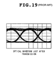
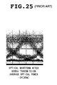
- an eye opening the area where an optical input signal can be surely distinguished into 1 or 0, is large, as shown in Fig. 19, while in the optical waveform after transmission of 600 km, the eye opening becomes very small, as shown in Fig. 25.
- the optimum decision threshold position for identifying 1 or 0 in the optical waveform varies depending on the light receiving power.
- the conventional optical transmission line has some tolerance of the decision threshold position to the distortion of the optical waveform, and even if the decision threshold position is fixed at a value adjusted by a maker at a shipment of the product, it is no problem practically.
- a first object of the present invention is to provide a decision threshold voltage control circuit of a decision threshold voltage feeding-capable clock and data recovery circuit and its decision threshold voltage controlling method, free from the occurrence of floor, capable of controlling a decision threshold position to the optimum one at each optical receiving level and improving the error rate characteristic much more than the conventional decision circuit where a decision point is fixed, by use of the digital calculation processing for the decision threshold voltage control circuit.
- a second object of the present invention is to provide a decision threshold voltage control circuit of a decision threshold voltage feeding-capable clock and data recovery circuit and its decision threshold voltage controlling method, capable of controlling a central decision point to the optimum position, by detecting an inner margin of the eye opening.
- a third object of the present invention is to provide a decision threshold voltage control circuit of a decision threshold voltage feeding-capable clock and data recovery circuit and its decision threshold voltage controlling method, capable of increasing measurement accuracy and escaping from a bad situation quickly, by adjusting the measurement time based on the measurement result of an error count unit.
- a fourth object of the present invention is to provide a decision threshold voltage control circuit of a decision threshold voltage feeding-capable clock and data recovery circuit and its decision threshold voltage controlling method, free from the necessity of using a large-sized counter in vain, by changing the measurement time depending on the number of the measured errors.
- a decision threshold voltage controlling method to feed an optimum decision threshold voltage to a clock and data recovery circuit which inputs an electric signal converted from an optical input signal and amplified with a predetermined amplitude as an input data signal, extracts a clock frequency component from the input data signal, and identifies 1 or 0 in the input data signal at a timing of the clock, the method comprising the steps of:
- a decision threshold voltage controlling method to feed an optimum decision threshold voltage to a clock and data recovery circuit which inputs an electric signal converted from an optical input signal and amplified with a predetermined amplitude as an input data signal, extracts a clock frequency component from the input data signal, and identifies 1 or 0 in the input data signal at a timing of the clock, the method comprising the steps of:
- a decision threshold voltage controlling method to feed an optimum decision threshold voltage to a clock and data recovery circuit which inputs an electric signal converted from an optical input signal and amplified with a predetermined amplitude as an input data signal, extracts a clock frequency component from the input data signal, and identifies 1 or 0 in the input data signal at a timing of the clock, the method comprising the steps of:
- a decision threshold voltage controlling method to feed an optimum decision threshold voltage to a clock and data recovery circuit which inputs an electric signal converted from an optical input signal and amplified with a predetermined amplitude as an input data signal, extracts a clock frequency component from the input data signal, and identifies 1 or 0 in the input data signal at a timing of the clock, the method comprising the steps of:
- a decision threshold voltage controlling method to feed an optimum decision threshold voltage to a clock and data recovery circuit which inputs an electric signal converted from an optical input signal and amplified with a predetermined amplitude as an input data signal, extracts a clock frequency component from the input data signal, and identifies 1 or 0 in the input data signal at a timing of the clock, the method comprising the steps of:
- the decision threshold voltage controlling method further comprises a step of moving the three decision points simultaneously, with the spaces between the respective upper and lower decision points and the central decision point kept as they are, depending on the measurement result of the errors.
- the decision threshold voltage controlling method further comprises a step of changing a time of measuring the number of the errors, depending on the measurement result of the errors.
- the decision threshold voltage controlling method further comprises a step of moving the three decision points simultaneously, with the spaces between the respective upper and lower decision points and the central decision point kept as they are, depending on the measurement result of the errors, and a step of changing a time of measuring the number of the errors, depending on the measurement result of the errors.
- a decision threshold voltage control circuit for feeding an optimum decision threshold voltage to a clock and data recovery circuit which inputs an electric signal converted from an optical input signal and amplified with a predetermined amplitude as an input data signal, extracts a clock frequency component from the input data signal, and identifies 1 or 0 in the input data signal at a timing of the clock, the circuit comprises means for controlling three decision points suitably, by selectively performing processing of controlling spaces of the three decision points, processing of moving the three decision points with their spaces kept as they are, and processing of changing an error pulse measurement time, depending on a measurement result of the error pulse.
- a decision threshold voltage control circuit for feeding an optimum decision threshold voltage to a clock and data recovery circuit which inputs an electric signal converted from an optical input signal and amplified with a predetermined amplitude as an input data signal, extracts a clock frequency component from the input data signal, and identifies 1 or 0 in the input data signal at a timing of the clock, the circuit comprises means for controlling three decision points suitably, by selectively performing processing of controlling spaces of the three decision points and processing of changing an error pulse measurement time, depending on a measurement result of the error pulse.
- a decision threshold voltage control circuit for feeding an optimum decision threshold voltage to a clock and data recovery circuit which inputs an electric signal converted from an optical input signal and amplified with a predetermined amplitude as an input data signal, extracts a clock frequency component from the input data signal, and identifies 1 or 0 in the input data signal at a timing of the clock, the circuit comprises means for controlling three decision points suitably, by selectively performing processing of controlling spaces of the three decision points and processing of moving the three decision points with their spaces kept as they are, depending on a measurement result of an error pulse.
- a decision threshold voltage control circuit for feeding an optimum decision threshold voltage to a clock and data recovery circuit which inputs an electric signal converted from an optical input signal and amplified with a predetermined amplitude as an input data signal, extracts a clock frequency component from the input data signal, and identifies 1 or 0 in the input data signal at a timing of the clock, the circuit comprises means for controlling three decision points suitably by controlling spaces of the three decision points, depending on a measurement result of an error pulse.
- a decision threshold voltage control circuit for feeding an optimum decision threshold voltage to a clock and data recovery circuit which inputs an electric signal converted from an optical input signal and amplified with a predetermined amplitude as an input data signal, extracts a clock frequency component from the input data signal, and identifies 1 or 0 in the input data signal at a timing of the clock
- the circuit comprises an error count unit of counting the number of errors at nearby H level and the number of errors at nearby L level of the input data signal, and a processing unit of changing a space between an upper decision point at the nearby H level and a central decision point, or a space between a lower decision point at the nearby L level and the central decision point, depending on the measurement result of the errors, wherein the central decision point is set at an optimum position while detecting an inner margin of an eye opening of the input data signal.
- the processing unit moves the three decision points simultaneously, with the spaces between the respective upper and lower decision points and the central decision point kept as they are, depending on the measurement result of the errors.
- the processing unit changes a time of measuring the number of the errors, depending on the measurement result of the errors.
- the processing unit moves the three decision points simultaneously, with the spaces between the respective upper and lower decision points and the central decision point kept as they are, depending on the measurement result of the errors, and changes a time of measuring the number of the errors, depending on the measurement result of the errors.
- a decision threshold voltage feeding-capable clock and data recovery circuit where a function of feeding a decision threshold voltage is added to a clock and data recovery circuit which inputs an electric signal converted from an optical input signal and amplified with a predetermined amplitude as an input data signal, extracts a clock frequency component from the input data signal, and identifies 1 or 0 in the input data signal at a timing of the clock, the circuit comprises a decision threshold voltage control circuit of controlling three decision points suitably, by selectively performing processing of controlling spaces of the three decision points, processing of moving the three decision points with their spaces kept as they are, and processing of changing an error pulse measurement time, depending on a measurement result of the error pulse.
- a decision threshold voltage feeding-capable clock and data recovery circuit where a function of feeding a decision threshold voltage is added to a clock and data recovery circuit which inputs an electric signal converted from an optical input signal and amplified with a predetermined amplitude as an input data signal, extracts a clock frequency component from the input data signal, and identifies 1 or 0 in the input data signal at a timing of the clock, the circuit comprises a decision threshold voltage control circuit of controlling three decision points suitably, by selectively performing processing of controlling spaces of the three decision points and processing of changing an error pulse measurement time, depending on a measurement result of the error pulse.
- a decision threshold voltage feeding-capable clock and data recovery circuit where a function of feeding a decision threshold voltage is added to a clock and data recovery circuit which inputs an electric signal converted from an optical input signal and amplified with a predetermined amplitude as an input data signal, extracts a clock frequency component from the input data signal, and identifies 1 or 0 in the input data signal at a timing of the clock, the circuit comprises a decision threshold voltage control circuit of controlling three decision points suitably, by selectively performing processing of controlling spaces of the three decision points and processing of moving the three decision points with their spaces kept as they are, depending on a measurement result of an error pulse.
- a decision threshold voltage feeding-capable clock and data recovery circuit where a function of feeding a decision threshold voltage is added to a clock and data recovery circuit which inputs an electric signal converted from an optical input signal and amplified with a predetermined amplitude as an input data signal, extracts a clock frequency component from the input data signal, and identifies 1 or 0 in the input data signal at a timing of the clock, the circuit comprises a decision threshold voltage control circuit of controlling three decision points suitably by controlling spaces of the three decision points, depending on a measurement result of an error pulse.
- a decision threshold voltage feeding-capable clock and data recovery circuit where a function of feeding a decision threshold voltage is added to a clock and data recovery circuit which inputs an electric signal converted from an optical input signal and amplified with a predetermined amplitude as an input data signal, extracts a clock frequency component from the input data signal, and identifies 1 or 0 in the input data signal at a timing of the clock, the circuit comprises an error count unit of counting the number of errors at nearby H level and the number of errors at nearby L level of the input data signal, a processing unit of changing a space between an upper decision point at the nearby H level and a central decision point, or a space between a lower decision point at the nearby L level and the central decision point, depending on the measurement result of the errors, and a decision threshold voltage control circuit of setting the central decision point at an optimum position while detecting an inner margin of an eye opening of the input data signal.
- the processing unit moves the three decision points simultaneously, with the spaces between the respective upper and lower decision points and the central decision point kept as they are, depending on the measurement result of the errors.
- the processing unit changes a time of measuring the number of the errors, depending on the measurement result of the errors.
- the processing unit moves the three decision points simultaneously, with the spaces between the respective upper and lower decision points and the central decision point kept as they are, depending on the measurement result of the errors, and changes a time of measuring the number of the errors, depending on the measurement result of the errors.
- a decision threshold voltage control program to feed an optimum decision threshold voltage to a clock and data recovery circuit which inputs an electric signal converted from an optical input signal and amplified with a predetermined amplitude as an input data signal, extracts a clock frequency component from the input data signal, and identifies 1 or 0 in the input data signal at a timing of the clock
- the program comprises a function of counting the number of errors at nearby H level and the number of errors at nearby L level of the input data signal, and a function of changing a space between an upper decision point at the nearby H level and a central decision point, or a space between a lower decision point at the nearby L level and the central decision point, depending on the measurement result of the errors, wherein the central decision point is set at an optimum position while detecting an inner margin of an eye opening of the input data signal.
- an optical receiver having an optical-to-electric converter of converting an optical input signal into an electric signal to supply it as an input data signal and a decision threshold voltage feeding-capable clock and data recovery circuit where a function of feeding a decision threshold voltage is added to a clock and data recovery circuit of extracting a clock component from the input data signal amplified with a predetermined amplitude and identifying 1 or 0 of the input data signal at a timing of the clock, the optical receiver comprises a decision threshold voltage control circuit of controlling three decision points suitably, by selectively performing processing of controlling spaces of the three decision points, processing of moving the three decision points with their spaces kept as they are, and processing of changing an error pulse measurement time, depending on a measurement result of the error pulse.
- an optical receiver having an optical-to-electric converter of converting an optical input signal into an electric signal to supply it as an input data signal and a decision threshold voltage feeding-capable clock and data recovery circuit where a function of feeding a decision threshold voltage is added to a clock and data recovery circuit of extracting a clock component from the input data signal amplified with a predetermined amplitude and identifying 1 or 0 of the input data signal at a timing of the clock, the optical receiver comprises a decision threshold voltage control circuit of controlling three decision points suitably, by selectively performing processing of controlling spaces of the three decision points and processing of changing an error pulse measurement time, depending on a measurement result of the error pulse.
- an optical receiver having an optical-to-electric converter of converting an optical input signal into an electric signal to supply it as an input data signal and a decision threshold voltage feeding-capable clock and data recovery circuit where a function of feeding a decision threshold voltage is added to a clock and data recovery circuit of extracting a clock component from the input data signal amplified with a predetermined amplitude and identifying 1 or 0 of the input data signal at a timing of the clock, the optical receiver comprises a decision threshold voltage control circuit of controlling three decision points suitably, by selectively performing processing of controlling spaces of the three decision points and processing of moving the three decision points with their spaces kept as they are, depending on a measurement result of an error pulse.
- an optical receiver having an optical-to-electric converter of converting an optical input signal into an electric signal to supply it as an input data signal and a decision threshold voltage feeding-capable clock and data recovery circuit where a function of feeding a decision threshold voltage is added to a clock and data recovery circuit of extracting a clock component from the input data signal amplified with a predetermined amplitude and identifying 1 or 0 of the input data signal at a timing of the clock, the optical receiver comprises a decision threshold voltage control circuit of controlling three decision points suitably by controlling spaces of the three decision points, depending on a measurement result of an error pulse.
- an optical receiver having an optical-to-electric converter of converting an optical input signal into an electric signal to supply it as an input data signal and a decision threshold voltage feeding-capable clock and data recovery circuit where a function of feeding a decision threshold voltage is added to a clock and data recovery circuit of extracting a clock component from the input data signal amplified with a predetermined amplitude and identifying 1 or 0 of the input data signal at a timing of the clock, the optical receiver comprises an error count unit of counting the number of errors at nearby H level and the number of errors at nearby L level of the input data signal, a processing unit of changing a space between an upper decision point at the nearby H level and a central decision point, or a space between a lower decision point at the nearby L level and the central decision point, depending on the measurement result of the errors, and a decision threshold voltage control circuit of setting the central decision point at an optimum position while detecting an inner margin of an eye opening of the input data signal.
- the processing unit moves the three decision points simultaneously, with the spaces between the respective upper and lower decision points and the central decision point kept as they are, depending on the measurement result of the errors, and changes a time of measuring the number of the errors, depending on the measurement result of the errors.
- a decision threshold voltage control circuit for feeding an optimum decision threshold voltage to a clock and data recovery circuit which inputs an electric signal converted from an optical input signal and amplified with a predetermined amplitude as an input data signal, extracts a clock frequency component from the input data signal, and identifies 1 or 0 in the input data signal at a timing of the clock
- the circuit comprises a D/A converter of generating a voltage depending on the number of errors at nearby H level and the number of errors at nearby L level of the input data signal, and a processing unit of changing a space between an upper decision point at the nearby H level and a central decision point, or a space between a lower decision point at the nearby L level and the central decision point, according to a voltage depending on the number of the errors, wherein the central decision point is set at an optimum position while detecting an inner margin of an eye opening of the input data signal.
- the processing unit further includes a first operational amplifier of determining a voltage in proportion to a difference voltage between a voltage corresponding to the number of the H level errors and a voltage corresponding to the number of the L level errors as a voltage corresponding to the central decision point, and a second operational amplifier of determining a voltage in inverse proportion to a voltage corresponding to the number of HL level errors as a voltage corresponding to the upper decision point and a voltage in proportion to the voltage corresponding to the number of the HL level errors as a voltage corresponding to the lower decision point.
- the processing unit includes a voltage divider of dividing the voltage corresponding to the upper decision point at the nearby H level and the voltage corresponding to the lower decision point at the nearly L level by some dividing ratio so as to supply a voltage corresponding to the central decision point.
- a decision threshold voltage control circuit for feeding an optimum decision threshold voltage to a clock and data recovery circuit which inputs an electric signal converted from an optical input signal and amplified with a predetermined amplitude as an input data signal, extracts a clock frequency component from the input data signal, and identifies 1 or 0 in the input data signal at a timing of the clock
- the circuit comprises a D/A converter of generating a voltage depending on the number of errors at nearby H level and the number of errors at nearby L level of the input data signal, and a processing unit of supplying each voltage corresponding to an upper decision point at nearby H level, a central decision point, and a lower decision point at nearby L level, according to a voltage corresponding to the number of the errors, while changing the spaces between the respective upper and lower decision points and the central decision point and moving the three decision points simultaneously with their spaces kept as they are, wherein the central decision point is set at an optimum position while detecting an inner margin of an eye opening of the input data signal.
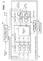
- Fig. 1 is a block diagram showing the structure of a decision threshold voltage control circuit of a decision threshold voltage feeding-capable CDR according to a first embodiment of the present invention.
- the reference numeral 100 designates decision threshold voltage feeding-capable CDR (clock and data recovery circuit) in which a function of feeding a decision threshold voltage is added to CDR that converts an optical input signal into an electric signal, extracts a clock component from the input data signal amplified to a predetermined amplitude, and discriminates 1 or 0 in the input data signal at the timing of the clock, and the reference numeral 10 designates a decision threshold voltage control circuit for feeding an optimum decision threshold voltage to the CDR according to a control algorithm, in the decision threshold voltage feeding-capable CDR 100.
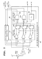
- the decision threshold voltage feeding-capable CDR 100 has been hitherto provided, and one example of its structure is shown in Fig. 2.
- error is detected by checking agreement or disagreement between the respective decision results of the adjacent decision points through the EXCLUSIVE-OR operation, and in the case of disagreement, an error pulse is supplied.
- the decision threshold voltage control circuit 10 comprises an error count unit 20, a processing unit 30 having a processing circuit 31, a measurement time setting unit 40, and a D/A converter 50.
- the error count unit 20 includes an H level error counter 21 and an L level error counter 22.
- An error pulse at nearby H level (hereinafter, referred to as H level error pulse) from the decision threshold voltage feeding-capable CDR 100 is counted by the H level error counter 21 and an error pulse at nearby L level (hereinafter, referred to as L level error pulse) therefrom is counted by the L level error counter 22.
- the processing circuit 31 of the processing unit 30 performs one or some of the following processes, depending on the number of the H level error pulses and the number of the L level error pulses.
- the measurement time setting unit 40 sets the measurement time of the error count unit at the optimum measurement time, depending on the number of the H level error pulses and the number of the L level error pulses.
- the D/A converter 50 converts a voltage at the upper decision point Vm, a voltage at the central decision point Vth, and a voltage at the lower decision point Vs respectively supplied from the processing unit, into respective analog voltages.
- the D/A converter 50 includes a D/A converting circuit 51 for converting the upper decision point voltage Vm into analog voltage, a D/A converting circuit 52 for converting the central decision point voltage Vth into analog voltage, and a D/A converting circuit 53 for converting the lower decision point voltage Vs into analog voltage.
- the decision threshold voltage control circuit and the decision threshold voltage feeding-capable CDR 100 have been described as separate circuits, needless to say, the decision threshold voltage control circuit may be built in the decision threshold voltage feeding-capable CDR 100.
- the decision threshold voltage feeding-capable CDR 100 includes three-value decision circuit 101 for identifying the upper decision point at nearby H level, the central decision point at nearby central level, and the lower decision point at nearby L level of the input data signal, a level fluctuation detecting circuit 102 for detecting level fluctuation and supplying the detected result to the decision threshold voltage control circuit 10, and a PLL circuit 103.
- the three-value decision circuit 101 is formed by comparators 110a, 110b, and 110c and flip-flops 120a, 120b, and 120c, and the level fluctuation detecting circuit 102 is formed by EXCLUSIVE-OR circuits 130a and 130b.
- the structure of an optical receiver to which the decision threshold voltage control circuit 10 according to the present invention is adopted is shown in Fig. 3.
- the optical receiver 200 includes an optical-to-electric converter 210 of receiving an optical data signal for converting it into an electric signal and supplying it as an input data signal, the above-mentioned decision threshold voltage feeding-capable CDR 100, and the decision threshold voltage control circuit 10, wherein a data signal having been identified is supplied from the decision threshold voltage feeding-capable CDR 100.
- Fig. 4 is a view showing the basic concept of a control algorithm in the processing unit 30 of the decision threshold voltage control circuit 10 which is characteristic of the present invention
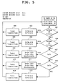
- Fig. 5 is one example of a flow chart by use of the control algorithm of the present invention
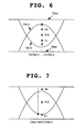
- Figs. 6 to 9 are views respectively showing the positional relationship among the eye opening, the upper decision point voltage Vm, the central decision point voltage Vth, and the lower decision point voltage Vs in each process of the flow chart of Fig. 5.
- the value of the central decision point voltage Vth may be set freely, being adjusted depending on the level and the data quality of an input optical data signal, namely, depending on a system adopting the decision threshold voltage feeding-capable CDR 100.
- Step 401 the first check in Step 401 is judged to be Y (Yes), and an operation of raising Vm by ⁇ Vm and lowering Vs by ⁇ Vs (widening the spaces between each decision point) is performed, in order to detect the margin of the eye opening (Step 402).
- This operation results in the state of Fig. 7.
- the measurement time Tsamp is extended by ⁇ Tsamp in order to increase the number of the error pulses counted within the measurement time for the purpose of enhancing the measuring accuracy (Step 403).
- the measurement time Tsamp is extended by ⁇ Tsamp in order to enhance the measurement accuracy (Step 409).
- the central decision point voltage Vth is near the optimum position in Fig. 8, the upper decision point voltage Vm and the lower decision point voltage Vs don't necessarily mean to detect the margin of the eye opening.
- the upper decision point voltage Vm is lowered by ⁇ Vm and the lower decision point voltage Vs is raised by ⁇ Vs in order to detect the margin of the eye opening (the space between each decision point is shrunken) (Step 413).
- the measurement time Tsamp is extended by ⁇ Tsamp similarly (Step 414).
- the embodiment can improve an error rate better than the conventional case of fixing the decision point, as illustrated in Fig. 26.
- the respective controls of the decision points and the respective controls of the error measurement time may be performed separately or simultaneously.
- a control of lowering the upper decision point voltage Vm by ⁇ Vm and raising the lower decision point voltage Vs by ⁇ Vs (the space between each decision point is shrunken) and a control of lowering the three points; the upper decision point voltage Vm, the central decision point voltage Vth, and the lower decision point voltage Vs by ⁇ Vth simultaneously may be performed at once.
- the upper decision point voltage Vm is lowered by ⁇ Vm and the lower decision point voltage Vs is raised by ⁇ Vs (the space between each decision point is shrunken), and the measurement time Tsamp is shortened by ⁇ Tsamp.
- the control of lowering the three points; the upper decision point voltage Vm, the central decision point voltage Vth, and the lower decision point voltage Vs by ⁇ Vth simultaneously is performed at the same time, this would enable a quicker escape from a bad state.
- the measurement time may be left as it is because the both numbers are adequate as the measured number.
- the order of the first check and the second check may be inverted and similarly the order of the third check and the fourth check may be inverted.
- the check may be performed in the order of the fist check (Step 401), the third check (Step 407) and the fourth check (Step 410) (or the fourth check and the third check), and the second check (Step 404). Or it may be performed in the order of the second check (Step 404), the third check (Step 407) and the fourth check (Step 410) (or the fourth check and the third check), and the first check (Step 401).
- the value ⁇ Vm need not be equal to the value ⁇ Vs.
- the central decision point voltage Vth proves to be in the middle of the upper decision point voltage Vm and the lower decision point voltage Vs.
- the values ⁇ Vm, ⁇ Vs, ⁇ Vth vary depending on how much degree to set the control accuracy.
- the values are set within the range of 1/10 to 1/1000 of an input data signal.
- the values of the Tsamp and ⁇ Tsamp also vary depending on how much degree to set the control accuracy.
- ⁇ Tsamp is set per 1/10 to 1/1000 of the above-mentioned time range, by way of example.
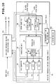
- Fig. 10 is a view showing the structure of the decision threshold voltage control circuit according to the second embodiment of the present invention
- Fig. 11 is a view showing the basic concept of a control algorithm according to the second embodiment
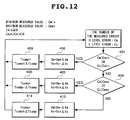
- Fig. 12 is one example of a flow chart by use of the control algorithm according to the second embodiment.
- the second embodiment is formed by simplifying the first embodiment, and it omits the process of simultaneously moving the three decision points with the spaces between the central decision point voltage Vth and the respective upper and lower decision point voltages Vm and Vs kept as they are, from the first embodiment.
- the step of moving the upper decision point voltage Vm and the lower decision point voltage Vs and the step of changing the error measurement time Tsamp are the same as the corresponding steps of Fig. 5.
- the central decision point voltage Vth is set at any point fixed between the upper decision point Vm and the lower decision point Vs by the processing unit 30. More specifically, after conversion into analog voltage, the central decision point voltage Vth is set at any point between the upper decision point voltage Vm and the lower decision point voltage Vs by using a voltage divider 60.
- Fig. 13 is a view showing the structure of the decision threshold voltage control circuit according to the third embodiment of the present invention
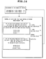
- Fig. 14 a view showing the basic concept of a control algorithm according to the third embodiment
- Fig. 15 is one example of a flow chart using the control algorithm according to the third embodiment.
- the third embodiment is constituted in that a fixed measurement time is set in the measurement time setting unit 40a, a count time is fixed in the error count unit 20, and that the error measurement time Tsamp is not changed, in the decision threshold voltage control circuit 10 according to the first embodiment.
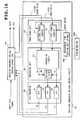
- FIG. 16 is a view showing the structure of the decision threshold voltage control circuit according to the fourth embodiment of the present invention
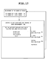
- Fig. 17 is a view showing the basic concept of a control algorithm according to the fourth embodiment
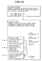
- Fig. 18 is one example of a flow chart using the control algorithm according to the fourth embodiment.
- the fourth embodiment is constituted in that the count time is fixed in the error count unit 20 and that the error measurement time Tsamp is not changed, in addition to the structure of the decision threshold voltage control circuit 10 according to the second embodiment.
- the controls of the decision threshold voltage control circuit 10 can be realized by forming each function of the control circuit by way of hardware. Further, they may be realized, by loading a decision threshold voltage control program that is a computer program having each function, into a memory of a computer.
- the decision threshold voltage control program is stored in a storing medium 600 such as a magnetic disk, a semiconductor memory, and the like. It is loaded from the storing medium into a computer, so to control the operation of the computer, thereby realizing each function of the above decision threshold voltage control circuit 10.
- Fig. 20 is a view showing the structure of the decision threshold voltage control circuit according to the fifth embodiment of the present invention
- Fig. 21 is a view showing the basic concept of a control algorithm according to the fifth embodiment.
- the upper decision point voltage Vm, the lower decision point voltage Vs, the central decision point voltage Vth are controlled in an analog fashion so as to be positioned at the optimum intervals.
- the decision threshold voltage control circuit 10A comprises a D/A converter 50A for converting the H level error pulses and the L level error pulses into the direct current voltages depending on the numbers of the respective level errors and a processing unit 30A.
- the processing unit 30A includes operational amplifiers 301A and 302A and the D/A converter 50A includes average value detecting circuits 501A to 503A and an OR-circuit 504A.
- the average value detecting circuit 501A converts the H level error pulses into the direct current voltages (H level error voltage Cm) depending on the number of the same error pulses
- the average value detecting circuit 502A converts the L level error pulses into the direct current voltages (L level error voltage Cs) depending on the number of the same error pulses
- the average value detecting circuit 503A converts the logical OR of the H level and the L level error pulses into the direct current voltages (HL level error voltage C) depending on the number of the error pulses of the logical OR, and the above direct current voltages are supplied to the processing unit 30A.
- the operational amplifier 301A determines a voltage in proportion to the difference voltage between the H level error voltage Cm and the L level error voltage Cs as the central decision point voltage Vth, and the operational amplifier 302A determines a voltage in inverse proportion to the HL level error voltage C as the upper decision point voltage Vm and a voltage in proportion to the HL level error voltage C as the lower decision point voltage Vs.
- the above processing is performed at once.
- the spaces of the three decision points; the upper decision point voltage Vm, the lower decision point voltage Vs, and the central decision point voltage Vth are controlled, thereby making it possible to adjust the respective decision points at the optimum positions.
- Fig. 22 is a view showing the structure of the decision threshold voltage control circuit according to the sixth embodiment of the present invention.
- the spaces between the respective upper and lower decision point voltages Vm and Vs and the central decision point voltage Vth are controlled and the three decision points are moved with their spaces kept as they are, hence to control the respective decision points to be placed at the optimum positions in an analog fashion.
- the decision threshold voltage control circuit 10B includes a D/A converter 50B for converting the H level error pulses and the L level error pulses into the direct current voltages depending on the numbers of the respective level errors and a processing unit 30B.
- the processing unit 30B includes operational amplifiers 301B, 302B, and 303B, and the D/A converter 50A includes average value detecting circuits 501B to 503B and an OR circuit 504B.
- the structure other than the processing unit 30B is the same as that of the fifth embodiment.
- the operational amplifier 301B determines a voltage in proportion to the difference voltage between the H level error voltage Cm and the L level error voltage Cs as the central decision point voltage Vth
- the operational amplifier 302B determines a voltage in proportion to the difference voltage between the HL level error voltage C and the central decision point voltage Vth as the upper decision point voltage Vm
- the operational amplifier 303B determines a voltage in proportion to the difference voltage between the HL level error voltage C and the voltage in inverse proportion to the difference voltage between the H level error voltage Cm and the L level error voltage Cs as the lower decision point voltage Vs.
- the upper decision point voltage Vm and the lower decision point voltage Vs also vary upward and downward accordingly.
- the spaces of the three decision points; the upper decision point voltage Vm, the lower decision point voltage Vs, and the central decision point voltage Vth are thus controlled and the three decision points are controlled to move while keeping the spaces thereof, thereby making it possible to adjust the decision points at the optimum positions.
- Fig. 23 is a view showing the structure of the decision threshold voltage control circuit according to the seventh embodiment of the present invention
- Fig. 24 is a view showing the basic concept of a control algorithm according to the seventh embodiment.
- the upper decision point voltage Vm, the lower decision point voltage Vs, and the central decision point voltage Vth are controlled to be placed at the optimum intervals in an analog fashion.
- the decision threshold voltage control circuit 10C comprises a D/A converter 50C for converting the H level error pulses and the L level error pulses into the direct current voltages depending on the numbers of the respective level errors, and a processing unit 30C.
- the processing unit 30C includes operational amplifiers 301C and 302C and a voltage divider 303C, and the D/A converter 50A includes average value detecting circuits 501C and 502C.
- the decision threshold voltage control circuit 10C only controls the space between the upper decision point voltage Vm and the lower decision point voltage Vs, and determines the central decision point voltage Vth through proportional distribution of the upper decision point voltage Vm and the lower decision point voltage Vs by the voltage divider 303C.
- the dividing ratio of the voltage divider 303C can be set at any value.
- the upper decision point voltage Vm when the H level error voltage Cm occurs, the upper decision point voltage Vm is controlled to be lowered, and when the L level error voltage Cs occurs, the lower decision point voltage Vs is controlled to be raised.
- the upper decision point voltage Vm, the lower decision point voltage Vs, and the central decision point voltage Vth are controlled to be placed at the optimum intervals.
- the measurement time may be set, depending on the power of the H level error voltage Cm and the L level error voltage Cs, similarly to the first embodiment.
- the present invention has been described by taking preferred embodiments for example, the present invention is not restricted to the above-mentioned embodiments, but it can be modified within the range of the technical sprit.
- the decision threshold voltage control circuit of the decision threshold voltage feeding-capable CDR and the decision threshold voltage control method of the present invention can achieve the following effects.
- the present invention can improve the error rate characteristic better than the conventional decision circuit in which the decision point is fixed, and it can prevent from floor.
- the measurement time is adjusted depending on the measurement result of the error count unit, it can enhance the measurement accuracy and escape from a bad state quickly.
Landscapes
- Engineering & Computer Science (AREA)
- Computer Networks & Wireless Communication (AREA)
- Signal Processing (AREA)
- Power Engineering (AREA)
- Physics & Mathematics (AREA)
- Electromagnetism (AREA)
- Dc Digital Transmission (AREA)
- Optical Communication System (AREA)
- Synchronisation In Digital Transmission Systems (AREA)
Abstract
Description
Claims (40)
- A decision threshold voltage controlling method to feed an optimum decision threshold voltage to a clock and data recovery circuit (100) which inputs an electric signal converted from an optical input signal and amplified with a predetermined amplitude as an input data signal, extracts a clock frequency component from the input data signal, and identifies 1 or 0 in the input data signal at a timing of the clock, the method comprising the steps of:a step of controlling three decision points suitably, by selectively performing a process of controlling spaces of the three decision points, a process of moving the three decision points with their spaces kept as they are, and a process of changing an error pulse measurement time, depending on a measurement result of the error pulse.
- A decision threshold voltage controlling method to feed an optimum decision threshold voltage to a clock and data recovery circuit (100) which inputs an electric signal converted from an optical input signal and amplified with a predetermined amplitude as an input data signal, extracts a clock frequency component from the input data signal, and identifies 1 or 0 in the input data signal at a timing of the clock, the method comprising the steps of:a step of controlling three decision points suitably, by selectively performing a process of controlling spaces of the three decision points and a process of changing an error pulse measurement time, depending on a measurement result of the error pulse.
- A decision threshold voltage controlling method to feed an optimum decision threshold voltage to a clock and data recovery circuit (100) which inputs an electric signal converted from an optical input signal and amplified with a predetermined amplitude as an input data signal, extracts a clock frequency component from the input data signal, and identifies 1 or 0 in the input data signal at a timing of the clock, the method comprising the steps of:a step of controlling three decision points suitably, by selectively performing a process of controlling spaces of the three decision points and a process of moving the three decision points with their spaces kept as they are, depending on a measurement result of an error pulse.
- A decision threshold voltage controlling method to feed an optimum decision threshold voltage to a clock and data recovery circuit (100) which inputs an electric signal converted from an optical input signal and amplified with a predetermined amplitude as an input data signal, extracts a clock frequency component from the input data signal, and identifies 1 or 0 in the input data signal at a timing of the clock, the method comprising the steps of:a step of controlling three decision points suitably by performing a process of controlling spaces of the three decision points, depending on a measurement result of an error pulse.
- A decision threshold voltage controlling method to feed an optimum decision threshold voltage to a clock and data recovery circuit (100) which inputs an electric signal converted from an optical input signal and amplified with a predetermined amplitude as an input data signal, extracts a clock frequency component from the input data signal, and identifies 1 or 0 in the input data signal at a timing of the clock, the method comprising the steps of:a step of counting the number of errors at nearby H level and the number of errors at nearby L level of the input data signal;a step of changing a space between an upper decision point at nearby H level and a central decision point, or a space between a lower decision point at nearby L level and the central decision point, depending on the measurement result of the errors; anda step of setting the central decision point at an optimum position while detecting an inner margin of an eye opening of the input data signal.
- The decision threshold voltage controlling method, as set forth in Claim 5, further comprising
a step of moving the three decision points simultaneously, with the spaces between the respective upper and lower decision points and the central decision point kept as they are, depending on the measurement result of the errors. - The decision threshold voltage controlling method, as set forth in Claim 5, further comprising
a step of changing a time of measuring the number of the errors, depending on the measurement result of the errors. - The decision threshold voltage controlling method, as set forth in Claim 5, further comprising:a step of moving the three decision points simultaneously, with the spaces between the respective upper and lower decision points and the central decision point kept as they are, depending on the measurement result of the errors; anda step of changing a time of measuring the number of the errors, depending on the measurement result of the errors.
- A decision threshold voltage control circuit for feeding an optimum decision threshold voltage to a clock and data recovery circuit (100) which inputs an electric signal converted from an optical input signal and amplified with a predetermined amplitude as an input data signal, extracts a clock frequency component from the input data signal, and identifies 1 or 0 in the input data signal at a timing of the clock, the circuit comprising:means for controlling three decision points suitably, by selectively performing processing of controlling spaces of the three decision points, processing of moving the three decision points with their spaces kept as they are, and processing of changing an error pulse measurement time, depending on a measurement result of the error pulse.
- A decision threshold voltage control circuit for feeding an optimum decision threshold voltage to a clock and data recovery circuit (100) which inputs an electric signal converted from an optical input signal and amplified with a predetermined amplitude as an input data signal, extracts a clock frequency component from the input data signal, and identifies 1 or 0 in the input data signal at a timing of the clock, the circuit comprising:means for controlling three decision points suitably, by selectively performing processing of controlling spaces of the three decision points and processing of changing an error pulse measurement time, depending on a measurement result of the error pulse.
- A decision threshold voltage control circuit for feeding an optimum decision threshold voltage to a clock and data recovery circuit (100) which inputs an electric signal converted from an optical input signal and amplified with a predetermined amplitude as an input data signal, extracts a clock frequency component from the input data signal, and identifies 1 or 0 in the input data signal at a timing of the clock, the circuit comprising:means for controlling three decision points suitably, by selectively performing processing of controlling spaces of the three decision points and processing of moving the three decision points with their spaces kept as they are, depending on a measurement result of an error pulse.
- A decision threshold voltage control circuit for feeding an optimum decision threshold voltage to a clock and data recovery circuit (100) which inputs an electric signal converted from an optical input signal and amplified with a predetermined amplitude as an input data signal, extracts a clock frequency component from the input data signal, and identifies 1 or 0 in the input data signal at a timing of the clock, the circuit comprising:means for controlling three decision points suitably by controlling spaces of the three decision points, depending on a measurement result of an error pulse.
- A decision threshold voltage control circuit for feeding an optimum decision threshold voltage to a clock and data recovery circuit (100) which inputs an electric signal converted from an optical input signal and amplified with a predetermined amplitude as an input data signal, extracts a clock frequency component from the input data signal, and identifies 1 or 0 in the input data signal at a timing of the clock, the circuit comprising:an error count unit (20) of counting the number of errors at nearby H level and the number of errors at nearby L level of the input data signal; anda processing unit (30) of changing a space between an upper decision point at the nearby H level and a central decision point, or a space between a lower decision point at the nearby L level and the central decision point, depending on the measurement result of the errors, whereinthe central decision point is set at an optimum position while detecting an inner margin of an eye opening of the input data signal.
- The decision threshold voltage control circuit, as set forth in Claim 13, wherein
further said processing unit (30)
moves the three decision points simultaneously, with the spaces between the respective upper and lower decision points and the central decision point kept as they are, depending on the measurement result of the errors. - The decision threshold voltage control circuit, as set forth in Claim 13, wherein
further said processing unit (30)
changes a time of measuring the number of the errors, depending on the measurement result of the errors. - The decision threshold voltage control circuit, as set forth in Claim 13, wherein
further said processing unit (30)
moves the three decision points simultaneously, with the spaces between the respective upper and lower decision points and the central decision point kept as they are, depending on the measurement result of the errors; and
changes a time of measuring the number of the errors, depending on the measurement result of the errors. - A decision threshold voltage feeding-capable clock and data recovery circuit where a function of feeding a decision threshold voltage is added to a clock and data recovery circuit (100) which inputs an electric signal converted from an optical input signal and amplified with a predetermined amplitude as an input data signal, extracts a clock frequency component from the input data signal, and identifies 1 or 0 in the input data signal at a timing of the clock, the circuit comprising:a decision threshold voltage control circuit (10) of controlling three decision points suitably, by selectively performing processing of controlling spaces of the three decision points, processing of moving the three decision points with their spaces kept as they are, and processing of changing an error pulse measurement time, depending on a measurement result of the error pulse.
- A decision threshold voltage feeding-capable clock and data recovery circuit where a function of feeding a decision threshold voltage is added to a clock and data recovery circuit (100) which inputs an electric signal converted from an optical input signal and amplified with a predetermined amplitude as an input data signal, extracts a clock frequency component from the input data signal, and identifies 1 or 0 in the input data signal at a timing of the clock, the circuit comprising:a decision threshold voltage control circuit (10) of controlling three decision points suitably, by selectively performing processing of controlling spaces of the three decision points and processing of changing an error pulse measurement time, depending on a measurement result of the error pulse.
- A decision threshold voltage feeding-capable clock and data recovery circuit where a function of feeding a decision threshold voltage is added to a clock and data recovery circuit (100) which inputs an electric signal converted from an optical input signal and amplified with a predetermined amplitude as an input data signal, extracts a clock frequency component from the input data signal, and identifies 1 or 0 in the input data signal at a timing of the clock, the circuit comprising:a decision threshold voltage control circuit (10) of controlling three decision points suitably, by selectively performing processing of controlling spaces of the three decision points and processing of moving the three decision points with their spaces kept as they are, depending on a measurement result of an error pulse.
- A decision threshold voltage feeding-capable clock and data recovery circuit where a function of feeding a decision threshold voltage is added to a clock and data recovery circuit (100) which inputs an electric signal converted from an optical input signal and amplified with a predetermined amplitude as an input data signal, extracts a clock frequency component from the input data signal, and identifies 1 or 0 in the input data signal at a timing of the clock, the circuit comprising:a decision threshold voltage control circuit (10) of controlling three decision points suitably by controlling spaces of the three decision points, depending on a measurement result of an error pulse.
- A decision threshold voltage feeding-capable clock and data recovery circuit where a function of feeding a decision threshold voltage is added to a clock and data recovery circuit (100) which inputs an electric signal converted from an optical input signal and amplified with a predetermined amplitude as an input data signal, extracts a clock frequency component from the input data signal, and identifies 1 or 0 in the input data signal at a timing of the clock, the circuit comprising:an error count unit (20) of counting the number of errors at nearby H level and the number of errors at nearby L level of the input data signal;a processing unit (30) of changing a space between an upper decision point at the nearby H level and a central decision point, or a space between a lower decision point at the nearby L level and the central decision point, depending on the measurement result of the errors; anda decision threshold voltage control circuit (10) of setting the central decision point at an optimum position while detecting an inner margin of an eye opening of the input data signal.
- The decision threshold voltage feeding-capable clock and data recovery circuit, as set forth in Claim 21, wherein
said processing unit (30)
moves the three decision points simultaneously, with the spaces between the respective upper and lower decision points and the central decision point kept as they are, depending on the measurement result of the errors. - The decision threshold voltage feeding-capable clock and data recovery circuit, as set forth in Claim 21, wherein
said processing unit (30)
changes a time of measuring the number of the errors, depending on the measurement result of the errors. - The decision threshold voltage feeding-capable clock and data recovery circuit, as set forth in Claim 21, wherein
said processing unit (30)
moves the three decision points simultaneously, with the spaces between the respective upper and lower decision points and the central decision point kept as they are, depending on the measurement result of the errors; and
changes a time of measuring the number of the errors, depending on the measurement result of the errors. - A decision threshold voltage control program to feed an optimum decision threshold voltage to a clock and data recovery circuit (100) which inputs an electric signal converted from an optical input signal and amplified with a predetermined amplitude as an input data signal, extracts a clock frequency component from the input data signal, and identifies 1 or 0 in the input data signal at a timing of the clock, the program comprising:a function of counting the number of errors at nearby H level and the number of errors at nearby L level of the input data signal; anda function of changing a space between an upper decision point at the nearby H level and a central decision point, or a space between a lower decision point at the nearby L level and the central decision point, depending on the measurement result of the errors, whereinthe central decision point is set at an optimum position while detecting an inner margin of an eye opening of the input data signal.
- The decision threshold voltage control program, as set forth in Claim 25, further comprising
a function of moving the three decision points simultaneously, with the spaces between the respective upper and lower decision points and the central decision point kept as they are, depending on the measurement result of the errors. - The decision threshold voltage control program, as set forth in Claim 25, further comprising
a function of changing a time of measuring the number of the errors, depending on the measurement result of the errors. - The decision threshold voltage control program, as set forth in Claim 25, further comprising
a function of moving the three decision points simultaneously, with the spaces between the respective upper and lower decision points and the central decision point kept as they are, depending on the measurement result of the errors; and
a function of changing a time of measuring the number of the errors, depending on the measurement result of the errors. - An optical receiver having an optical-to-electric converter of converting an optical input signal into an electric signal to supply it as an input data signal and a decision threshold voltage feeding-capable clock and data recovery circuit (100) where a function of feeding a decision threshold voltage is added to a clock and data recovery circuit of extracting a clock component from the input data signal amplified with a predetermined amplitude and identifying 1 or 0 of the input data signal at a timing of the clock, the optical receiver comprising:a decision threshold voltage control circuit (10) of controlling three decision points suitably, by selectively performing processing of controlling spaces of the three decision points, processing of moving the three decision points with their spaces kept as they are, and processing of changing an error pulse measurement time, depending on a measurement result of the error pulse.
- An optical receiver having an optical-to-electric converter of converting an optical input signal into an electric signal to supply it as an input data signal and a decision threshold voltage feeding-capable clock and data recovery circuit (100) where a function of feeding a decision threshold voltage is added to a clock and data recovery circuit of extracting a clock component from the input data signal amplified with a predetermined amplitude and identifying 1 or 0 of the input data signal at a timing of the clock, the optical receiver comprising:a decision threshold voltage control circuit (10) of controlling three decision points suitably, by selectively performing processing of controlling spaces of the three decision points and processing of changing an error pulse measurement time, depending on a measurement result of the error pulse.
- An optical receiver having an optical-to-electric converter of converting an optical input signal into an electric signal to supply it as an input data signal and a decision threshold voltage feeding-capable clock and data recovery circuit (100) where a function of feeding a decision threshold voltage is added to a clock and data recovery circuit of extracting a clock component from the input data signal amplified with a predetermined amplitude and identifying 1 or 0 of the input data signal at a timing of the clock, the optical receiver comprising:a decision threshold voltage control circuit (10) of controlling three decision points suitably, by selectively performing processing of controlling spaces of the three decision points and processing of moving the three decision points with their spaces kept as they are, depending on a measurement result of an error pulse.
- An optical receiver having an optical-to-electric converter of converting an optical input signal into an electric signal to supply it as an input data signal and a decision threshold voltage feeding-capable clock and data recovery circuit (100) where a function of feeding a decision threshold voltage is added to a clock and data recovery circuit of extracting a clock component from the input data signal amplified with a predetermined amplitude and identifying 1 or 0 of the input data signal at a timing of the clock, the optical receiver comprising:a decision threshold voltage control circuit (10) of controlling three decision points suitably by controlling spaces of the three decision points, depending on a measurement result of an error pulse.
- An optical receiver having an optical-to-electric converter of converting an optical input signal into an electric signal to supply it as an input data signal and a decision threshold voltage feeding-capable clock and data recovery circuit (100) where a function of feeding a decision threshold voltage is added to a clock and data recovery circuit of extracting a clock component from the input data signal amplified with a predetermined amplitude and identifying 1 or 0 of the input data signal at a timing of the clock, the optical receiver comprising:an error count unit (20) of counting the number of errors at nearby H level and the number of errors at nearby L level of the input data signal;a processing unit (30) of changing a space between an upper decision point at the nearby H level and a central decision point, or a space between a lower decision point at the nearby L level and the central decision point, depending on the measurement result of the errors; anda decision threshold voltage control circuit (10) of setting the central decision point at an optimum position while detecting an inner margin of an eye opening of the input data signal.
- The optical receiver, as set forth in Claim 33, wherein
said processing unit (10)
moves the three decision points simultaneously, with the spaces between the respective upper and lower decision points and the central decision point kept as they are, depending on the measurement result of the errors. - The optical receiver, as set forth in Claim 33, wherein
said processing unit (30)
changes a time of measuring the number of the errors, depending on the measurement result of the errors. - The optical receiver, as set forth in Claim 33, wherein
said processing unit (30)
moves the three decision points simultaneously, with the spaces between the respective upper and lower decision points and the central decision point kept as they are, depending on the measurement result of the errors; and
changes a time of measuring the number of the errors, depending on the measurement result of the errors. - A decision threshold voltage control circuit for feeding an optimum decision threshold voltage to a clock and data recovery circuit (100) which inputs an electric signal converted from an optical input signal and amplified with a predetermined amplitude as an input data signal, extracts a clock frequency component from the input data signal, and identifies 1 or 0 in the input data signal at a timing of the clock, the circuit comprising:a D/A converter (50) of generating a voltage depending on the number of errors at nearby H level and the number of errors at nearby L level of the input data signal; anda processing unit (30) of changing a space between an upper decision point at the nearby H level and a central decision point, or a space between a lower decision point at the nearby L level and the central decision point, according to a voltage depending on the number of the errors, whereinthe central decision point is set at an optimum position while detecting an inner margin of an eye opening of the input data signal.
- The decision threshold voltage control circuit, as set forth in Claim 37, wherein
said processing unit (30) further includes
a first operational amplifier (301A, 301B, 301C) of determining a voltage in proportion to a difference voltage between a voltage corresponding to the number of the H level errors and a voltage corresponding to the number of the L level errors as a voltage corresponding to the central decision point, and
a second operational amplifier (302A, 302B, 302C) of determining a voltage in inverse proportion to a voltage corresponding to the number of HL level errors as a voltage corresponding to the upper decision point and a voltage in proportion to the voltage corresponding to the number of the HL level errors as a voltage corresponding to the lower decision point. - The decision threshold voltage control circuit, as set forth in Claim 37, wherein
said processing unit (30) includes
a voltage divider (60, 303C) of dividing the voltage corresponding to the upper decision point at the nearby H level and the voltage corresponding to the lower decision point at the nearly L level by some dividing ratio so as to supply a voltage corresponding to the central decision point. - A decision threshold voltage control circuit for feeding an optimum decision threshold voltage to a clock and data recovery circuit which inputs an electric signal converted from an optical input signal and amplified with a predetermined amplitude as an input data signal, extracts a clock frequency component from the input data signal, and identifies 1 or 0 in the input data signal at a timing of the clock, the circuit comprising:a D/A converter (50) of generating a voltage depending on the number of errors at nearby H level and the number of errors at nearby L level of the input data signal; anda processing unit (30) of supplying each voltage corresponding to an upper decision point at nearby H level, a central decision point, and a lower decision point at nearby L level, according to a voltage corresponding to the number of the errors, while changing the spaces between the respective upper and lower decision points and the central decision point and moving the three decision points simultaneously with their spaces kept as they are, whereinthe central decision point is set at an optimum position while detecting an inner margin of an eye opening of the input data signal.
Applications Claiming Priority (2)
| Application Number | Priority Date | Filing Date | Title |
|---|---|---|---|
| JP2001076455A JP3652995B2 (en) | 2001-03-16 | 2001-03-16 | Identification voltage control circuit, identification voltage control method, optical receiver, identification voltage control program for clock data recovery circuit |
| JP2001076455 | 2001-03-16 |
Publications (2)
| Publication Number | Publication Date |
|---|---|
| EP1241845A2 true EP1241845A2 (en) | 2002-09-18 |
| EP1241845A3 EP1241845A3 (en) | 2006-08-02 |
Family
ID=18933382
Family Applications (1)
| Application Number | Title | Priority Date | Filing Date |
|---|---|---|---|
| EP02005365A Withdrawn EP1241845A3 (en) | 2001-03-16 | 2002-03-14 | Control of decision thresholds in a receiver of an optical transmission system |
Country Status (3)
| Country | Link |
|---|---|
| US (1) | US7218686B2 (en) |
| EP (1) | EP1241845A3 (en) |
| JP (1) | JP3652995B2 (en) |
Cited By (1)
| Publication number | Priority date | Publication date | Assignee | Title |
|---|---|---|---|---|
| EP1630983A4 (en) * | 2003-06-03 | 2009-01-28 | Fujitsu Ltd | OPTICAL SIGNAL RECEIVING DEVICE AND SCANNING DISCRIMINATION POINT CONTROL METHOD THEREOF |
Families Citing this family (10)
| Publication number | Priority date | Publication date | Assignee | Title |
|---|---|---|---|---|
| WO2004098120A1 (en) * | 2003-05-01 | 2004-11-11 | Mitsubishi Denki Kabushiki Kaisha | Clock data recovery circuit |
| US7590175B2 (en) | 2003-05-20 | 2009-09-15 | Rambus Inc. | DFE margin test methods and circuits that decouple sample and feedback timing |
| US7336749B2 (en) * | 2004-05-18 | 2008-02-26 | Rambus Inc. | Statistical margin test methods and circuits |
| US7627029B2 (en) | 2003-05-20 | 2009-12-01 | Rambus Inc. | Margin test methods and circuits |
| US7408981B2 (en) * | 2003-05-20 | 2008-08-05 | Rambus Inc. | Methods and circuits for performing margining tests in the presence of a decision feedback equalizer |
| GB2402841B (en) * | 2003-06-10 | 2005-05-11 | Whereonearth Ltd | A method of providing location based information to a mobile terminal within a communications network |
| US7643759B2 (en) * | 2005-01-12 | 2010-01-05 | Sumitomo Electric Industries, Ltd. | Signal-quality evaluation device, signal adjustment method, optical-signal evaluation system, and optical transmission system |
| US8249447B2 (en) * | 2008-04-29 | 2012-08-21 | Menara Networks, Inc. | Systems and methods for optical receiver decision threshold optimization |
| WO2010067448A1 (en) * | 2008-12-11 | 2010-06-17 | 富士通株式会社 | Reception device, transmission device, and transmission method |
| US8713380B2 (en) * | 2011-05-03 | 2014-04-29 | SanDisk Technologies, Inc. | Non-volatile memory and method having efficient on-chip block-copying with controlled error rate |
Family Cites Families (21)
| Publication number | Priority date | Publication date | Assignee | Title |
|---|---|---|---|---|
| FR2511566A1 (en) * | 1981-08-12 | 1983-02-18 | Thomson Csf | THRESHOLD OPTICAL RECEIVER FOR DIGITAL RATE DIGITAL TRANSMISSION SYSTEM |
| JPS60178751A (en) | 1984-02-24 | 1985-09-12 | Fujitsu Ltd | Detection circuit for signal deterioration |
| JP2571408B2 (en) | 1987-12-11 | 1997-01-16 | 富士通株式会社 | Test methods for communication systems |
| US4823360A (en) * | 1988-02-12 | 1989-04-18 | Northern Telecom Limited | Binary data regenerator with adaptive threshold level |
| JP2530904B2 (en) * | 1988-02-22 | 1996-09-04 | 富士通株式会社 | Optimal discrimination level control method |
| JPH0454043A (en) | 1990-06-22 | 1992-02-21 | Fujitsu Ltd | Reception data identification circuit |
| US5521941A (en) * | 1990-11-29 | 1996-05-28 | Motorola, Inc. | Automatic threshold control for multi-level signals |
| JP2598913Y2 (en) * | 1992-07-27 | 1999-08-23 | ミツミ電機株式会社 | Data slicer |
| JPH0810851B2 (en) | 1993-01-11 | 1996-01-31 | 日本電気株式会社 | Waveform identification device |
| US5425056A (en) * | 1993-03-23 | 1995-06-13 | Motorola, Inc. | Method and apparatus for generating threshold levels in a radio communication device for receiving four-level signals |
| FR2731125B1 (en) * | 1995-02-28 | 1997-05-16 | Sgs Thomson Microelectronics | CIRCUIT FOR PROCESSING AN ASYNCHRONOUS SIGNAL PERIODICALLY PRESENTING SYNCHRONIZATION SALVES |
| JP3551393B2 (en) | 1995-03-20 | 2004-08-04 | 富士通株式会社 | Identification circuit |
| US5670951A (en) * | 1995-07-17 | 1997-09-23 | Motorola, Inc. | Radio communication device and method for generating threshold levels in a radio communication device for receiving four-level signals |
| JPH09205466A (en) * | 1996-01-29 | 1997-08-05 | Kokusai Electric Co Ltd | Symbol determination device |
| JPH1093641A (en) * | 1996-09-12 | 1998-04-10 | Nec Corp | Multivalued fsk demodulation window comparator |
| JP3863265B2 (en) * | 1997-10-16 | 2006-12-27 | 富士通株式会社 | Optical receiver and clock extraction circuit |
| US6188737B1 (en) * | 1999-11-24 | 2001-02-13 | Nortel Networks Limited | Method and apparatus for regenerating data |
| CA2328251C (en) * | 1999-12-15 | 2004-05-25 | Nec Corporation | Automatic identification level control circuit, identification level control method, automatic identification phase control circuit, identification phase control method, optical receiver, and optical communication system |
| JP3657209B2 (en) | 2000-10-26 | 2005-06-08 | 三菱電機株式会社 | Anomaly detection circuit for optical receiver and optical receiver |
| JP3731505B2 (en) * | 2001-07-18 | 2006-01-05 | 日本電気株式会社 | Optical receiver, optical data signal waveform optimization method, and optical data signal waveform optimization program |
| JP3856101B2 (en) * | 2001-09-03 | 2006-12-13 | 日本電気株式会社 | Optical receiver having reception waveform shaping function |
-
2001
- 2001-03-16 JP JP2001076455A patent/JP3652995B2/en not_active Expired - Fee Related
-
2002
- 2002-03-14 EP EP02005365A patent/EP1241845A3/en not_active Withdrawn
- 2002-03-15 US US10/097,394 patent/US7218686B2/en not_active Expired - Fee Related
Cited By (1)
| Publication number | Priority date | Publication date | Assignee | Title |
|---|---|---|---|---|
| EP1630983A4 (en) * | 2003-06-03 | 2009-01-28 | Fujitsu Ltd | OPTICAL SIGNAL RECEIVING DEVICE AND SCANNING DISCRIMINATION POINT CONTROL METHOD THEREOF |
Also Published As
| Publication number | Publication date |
|---|---|
| JP2002281094A (en) | 2002-09-27 |
| US7218686B2 (en) | 2007-05-15 |
| EP1241845A3 (en) | 2006-08-02 |
| JP3652995B2 (en) | 2005-05-25 |
| US20020131531A1 (en) | 2002-09-19 |
Similar Documents
| Publication | Publication Date | Title |
|---|---|---|
| JP3731505B2 (en) | Optical receiver, optical data signal waveform optimization method, and optical data signal waveform optimization program | |
| EP1241845A2 (en) | Control of decision thresholds in a receiver of an optical transmission system | |
| US7796176B2 (en) | Phase adjusting device, phase adjusting method, and digital camera | |
| US7254345B2 (en) | Receiver and receiving method capable of detecting an eye aperture size formed by reception data signals | |
| US7433440B2 (en) | Jitter-detecting circuit, receiving circuit including the jitter-detecting circuit, and communication system | |
| US20110063689A1 (en) | Image reading apparatus and image forming apparatus | |
| US8508810B2 (en) | Image reading apparatus and image forming apparatus | |
| CN101064770B (en) | Image processing method and image processing circuit | |
| US20040125874A1 (en) | Method of determining an eye diagram of a digital signal | |
| US7724090B2 (en) | Loop control apparatus and method thereof | |
| US20070280079A1 (en) | Asymmetry measurement apparatus | |
| US10651949B1 (en) | Calibration for an optical communications link | |
| US20060279440A1 (en) | Frequency detector in phase locked loop circuit and frequency error detecting method | |
| EP1641165A1 (en) | Optical reception device and optical reception method | |
| US6345020B1 (en) | Apparatus and method for generating a tracking error signal using first through fourth optical detector elements | |
| US6967906B2 (en) | Circuit and method for detecting mirror signal for optical disc apparatus | |
| KR0134487B1 (en) | Peripheral contrast correction circuitry on the camcorder screen | |
| US7606487B1 (en) | Distortion measurement in optical communication systems | |
| KR102563390B1 (en) | Method for automatically adjusting the magnetic field measurement step and range of a geomagnetic sensor | |
| KR100447663B1 (en) | Device for automatically controlling a cdp focus offset and a method therefor, particularly enabling a reliable automatic control for abnormal conditions such as scars and dust of a disk | |
| US7336571B2 (en) | Method and arrangement for compensating scanning disturbances on optical recording media | |
| US5748023A (en) | Integrator with output-compensating capability | |
| US6807135B1 (en) | Tilt detection system, tilt detection method and tilt adjustment method | |
| US20050128007A1 (en) | Preamplifier circuit, clock switching circuit, and optical receiver | |
| JP2003069500A (en) | Optical receiver with function of adjusting multiplication factor of light receiving element |
Legal Events
| Date | Code | Title | Description |
|---|---|---|---|
| PUAI | Public reference made under article 153(3) epc to a published international application that has entered the european phase |
Free format text: ORIGINAL CODE: 0009012 |
|
| AK | Designated contracting states |
Kind code of ref document: A2 Designated state(s): AT BE CH CY DE DK ES FI FR GB GR IE IT LI LU MC NL PT SE TR |
|
| AX | Request for extension of the european patent |
Free format text: AL;LT;LV;MK;RO;SI |
|
| PUAL | Search report despatched |
Free format text: ORIGINAL CODE: 0009013 |
|
| AK | Designated contracting states |
Kind code of ref document: A3 Designated state(s): AT BE CH CY DE DK ES FI FR GB GR IE IT LI LU MC NL PT SE TR |
|
| AX | Request for extension of the european patent |
Extension state: AL LT LV MK RO SI |
|
| 17P | Request for examination filed |
Effective date: 20060712 |
|
| AKX | Designation fees paid |
Designated state(s): DE GB |
|
| 17Q | First examination report despatched |
Effective date: 20071025 |
|
| STAA | Information on the status of an ep patent application or granted ep patent |
Free format text: STATUS: THE APPLICATION IS DEEMED TO BE WITHDRAWN |
|
| 18D | Application deemed to be withdrawn |
Effective date: 20080306 |