EP1241728A2 - Compact primary radiator - Google Patents
Compact primary radiator Download PDFInfo
- Publication number
- EP1241728A2 EP1241728A2 EP02251064A EP02251064A EP1241728A2 EP 1241728 A2 EP1241728 A2 EP 1241728A2 EP 02251064 A EP02251064 A EP 02251064A EP 02251064 A EP02251064 A EP 02251064A EP 1241728 A2 EP1241728 A2 EP 1241728A2
- Authority
- EP
- European Patent Office
- Prior art keywords
- waveguide
- probe
- radiation pattern
- circuit board
- probes
- Prior art date
- Legal status (The legal status is an assumption and is not a legal conclusion. Google has not performed a legal analysis and makes no representation as to the accuracy of the status listed.)
- Withdrawn
Links
Images

Classifications
-
- H—ELECTRICITY
- H01—ELECTRIC ELEMENTS
- H01P—WAVEGUIDES; RESONATORS, LINES, OR OTHER DEVICES OF THE WAVEGUIDE TYPE
- H01P1/00—Auxiliary devices
- H01P1/16—Auxiliary devices for mode selection, e.g. mode suppression or mode promotion; for mode conversion
- H01P1/161—Auxiliary devices for mode selection, e.g. mode suppression or mode promotion; for mode conversion sustaining two independent orthogonal modes, e.g. orthomode transducer
Definitions
- the present invention relates to a primary radiator for allowing a pair of probes disposed in a waveguide to selectively extract a vertically polarized wave and a horizontally polarized wave which are orthogonal to each other, and in particular, to a primary radiator having the pair of probes formed on a circuit board partly disposed in the waveguide.
- the left-hand and right-hand circularly polarized waves are introduced into a waveguide and are converted into a vertically polarized wave and a horizontally polarized wave, respectively, at a 90-degree shifter, a pair of probes selectively extracts these polarized waves, and a converter circuit of the converter converts the frequencies of the received signals from the probes into signals having intermediate frequencies, thus allowing the converter to output the frequency-converted signals.
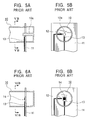
- an exemplary configuration of the known probes is such that a waveguide 10 has a circuit board 11 disposed therein, which is orthogonal to the axis of the waveguide 10, and a cylindrical stub 10a disposed in a projecting manner on the terminal face thereof, and the circuit board 11 has a probe 12 and a probe 13, formed by patterning, on the same surface thereof for the vertically and horizontally polarized waves, respectively.
- the two probes 12 and 13 are formed by patterning on the same surface of the circuit board 11, thereby allowing the waveguide 10 to be shortened in the axial direction thereof, and moreover, the stub 10a disposed in a projecting manner on the terminal face of the waveguide 10 achieves sufficient isolation between the vertically and horizontally polarized waves.
- FIG. 6 another exemplary configuration of the known probes is such that a fine radiation pattern 14 is formed in place of the above stub 10a on the same surface of the circuit board 11 as that on which the probes 12 and 13 are formed.
- This fine radiation pattern 14 is square or circular and is asymmetrical relative to each of the axes of the probes 12 and 13.
- the fine radiation pattern 14 achieves sufficient isolation between the vertically and horizontally polarized waves while providing an advantage in that the waveguide 10 is shortened in the axial direction thereof.
- the probe configuration shown in Fig. 5 has a problem in that forming an elongated stub on the terminal face of the waveguide in a projecting manner makes the waveguide structure complicated, and in particular, when the waveguide is formed from a metal plate, this makes it extremely difficult to form the stub on the metal plate.
- the probe configuration shown in Fig. 5 has a problem in that eliminating the above stub makes the waveguide structure simple, the probe configuration shown in Fig.
- a primary radiator comprises the following elements: a waveguide for transmitting a vertically polarized wave and a horizontally polarized wave which are orthogonal to each other; a circuit board disposed in the waveguide so as to be orthogonal to the axis of the waveguide; a fine radiation pattern formed on the circuit board in the vicinity of the axis of the waveguide; and a first probe and a second probe formed on the circuit board and extending from the inner wall of the waveguide toward the fine radiation pattern.
- the first probe and the second probe are substantially orthogonal to each other, and the fine radiation pattern is electrically slanted at about 45 degrees relative to each of the axes of the first probe and the second probe.
- the fine radiation pattern formed on the circuit board by disposing the fine radiation pattern formed on the circuit board so as to be electrically slanted at about 45 degrees relative to each of the axes of the first and second probes, the fine radiation pattern prevents the electric field of the vertically and horizontally polarized waves in the waveguide from being disturbed, thus leading to a reduction in reflection of these polarized waves thereat while maintaining sufficient isolation between these polarized waves.
- the fine radiation pattern may have a strip shape, such as a rectangular shape and an elliptical shape, extending along a direction slanted at about 45 degrees relative to each of the axes of the first probe and the second probe.
- the fine radiation pattern may have an L-shape having a first arm and a second arm which are substantially orthogonal to each other and which are electrically slanted at about 45 degrees relative to each of the axes of the first probe and the second probe.
- thee present invention has the following advantages.
- a circuit board is disposed in a waveguide, in which a vertically polarized wave and a horizontally polarized wave propagate, so as to be orthogonal to the axis of the waveguide, has a first probe and a second probe formed thereon for respectively extracting the vertically and horizontally polarized waves, and also has a fine radiation pattern formed thereon electrically slanted at about 45 degrees relative to each of the axes of the first and second probes.
- This configuration allows a fine radiation pattern having a relatively small size to prevent the electric field of the vertically and horizontally polarized waves in the waveguide from being disturbed and also these polarized waves from being reflected thereat, while maintaining sufficient isolation between these polarized waves.
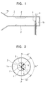
- Fig. 1 is a schematic sectional view illustrating a primary radiator according to an embodiment of the present invention.
- Fig. 2 is an elevational view of the primary radiator viewed from a horn of the primary radiator.
- Fig. 3 is an illustration of a circuit board provided in the primary radiator.
- the primary radiator comprises a tubular waveguide 1 having a horn 1a at one end and a terminal face 1b at the other end, a pair of ridges 2 projecting from the inner wall of the waveguide 1 toward the axis of the waveguide 1, and a circuit board 3 partly inserted in the waveguide 1, wherein the plane of the circuit board 3 is orthogonal to the waveguide axis.
- the pair of ridges 2 serves as a 90-degree phase shifter so that a left-hand circularly polarized wave and a right-hand circularly polarized wave entering the waveguide 1 are converted to a vertically polarized wave and a horizontally polarized wave, respectively.
- a dielectric plate may be used as a 90-degree phase shifter instead of the pair of ridges 2.
- the circuit board 3 has a plurality of perforations 4 perforated therethrough and lying inside the waveguide 1 for forming a first bridge 3a, a second bridge 3b, and a third bridge 3c.
- the first and second bridges 3a and 3b intersect with each other at about 90 degrees and extend from the inner wall of the waveguide 1 toward the axis of the waveguide so as to connect to the third bridge 3c.
- the third bridge 3c intersects each of the first and second bridges 3a and 3b at about 45 degrees and extends between opposing points on the inner wall of the waveguide 1.
- a first probe 5 lying on the first bridge 3a, a second probe 6 lying on the second bridge 3b, and a fine radiation pattern 7 lying on the third bridge 3c are formed by patterning.
- a grounding pattern is formed thereon except the areas for the first to third bridges 3a to 3c.
- another grounding pattern a micro-strip wiring, circuit elements for a converter circuit, and so forth are formed. These grounding patterns formed on both sides of the circuit board 3 are electrically connected to each other via through-holes.
- the circuit board 3 is separated from the terminal face 1b of the waveguide 1 by about a quarter of the wavelength in waveguide.
- the terminal face 1b serves as a reflection surface of the probes 5 and 6.
- the first and second probes 5 and 6 respectively receive the vertically and horizontally polarized waves propagating in the waveguide 1 and are substantially orthogonal to each other in the waveguide 1.
- the probes 5 and 6 are set to intersect with each other at an angle slightly smaller that 90 degrees so that the leading edges of the probes 5 and 6 are kept as far away from each other as possible.
- a plane including the axis of the waveguide 1 and the two ridges 2 is designated as a reference plane P
- the probes 5 and 6 each intersect the reference plane P at about 45 degrees.
- the fine radiation pattern 7 has a rectangular shape extending substantially parallel to the reference plane P and opposes the leading edges of the probes 5 and 6 on the circuit board 3 while keeping a predetermined distance away from these leading edges.
- the fine radiation pattern 7 has a longitudinal axis intersecting each of the axes of the probes 5 and 6 at about 45 degrees and is formed to be asymmetrical relative to each of the axes of the probes 5 and 6.
- a left-hand circularly polarized wave and a right-hand circularly polarized wave transmitted from a satellite enter the waveguide 1 via the horn 1a and are converted to linearly polarized waves by the two ridges 2 while propagating in the waveguide 1.
- a circularly polarized wave is a rotating polarized wave that is a combination of the vectors of two linearly polarized waves that have the same amplitude and a 90-degree phase difference from each other.
- the circularly polarized wave having the above 90-degree phase difference is converted to the polarized wave having a common mode while passing through the two ridges 2, for example, the left-hand circularly polarized wave is converted to a vertically polarized wave and the right-hand circularly polarized wave is converted to a horizontally polarized wave.
- the first and second probes 5 and 6 respectively extract the vertically and horizontally polarized waves travelling in the waveguide 1 toward the terminal face 1b.
- a converter circuit converts the frequencies of the output signals of the probes 5 and 6 into intermediate frequency signals, thus allowing the left-hand circularly and right-hand circularly polarized waves to be received.
- the fine radiation pattern 7 is formed on the circuit board 3 so as to oppose the leading edges of the probes 5 and 6 at a predetermined distance, and intersects each of the axes of the probes 5 and 6 at about 45 degrees.
- This configuration allows the fine radiation pattern 7 to prevent the electric field of the vertically and horizontally polarized waves from being disturbed, thus achieving sufficient isolation between the vertically and horizontally polarized waves.
- the fine radiation pattern 7 is rectangular and asymmetrical relative to each of the axes of the probes 5 and 6, and also is set to have a relatively small size, i.e., a relatively small area, thus preventing the vertically and horizontally polarized waves from being reflected thereat, while maintaining sufficient isolation between these polarized waves.
- the fine radiation pattern 7 is not limited to having a rectangular shape in the foregoing embodiment, but may have an elliptical shape or a crescent shape, as shown in Fig. 4A or Fig. 4B, respectively.
- the fine radiation pattern 7 may have an L-shape having two arms 7a and 7b which are substantially orthogonal to each other and which are electrically slanted at about 45 degrees relative to each of the axes of the probes 5 and 6. The point is that the fine radiation pattern 7 is electrically slanted at about 45 degrees relative to each of the axes of the first and second probes 5 and 6.
Landscapes
- Waveguide Aerials (AREA)
- Variable-Direction Aerials And Aerial Arrays (AREA)
- Waveguide Switches, Polarizers, And Phase Shifters (AREA)
Abstract
Description
Claims (3)
- A primary radiator comprising:wherein the first probe and the second probe are substantially orthogonal to each other, and the fine radiation pattern is electrically slanted at about 45 degrees relative to each of the axes of the first probe and the second probe.a waveguide for transmitting a vertically polarized wave and a horizontally polarized wave which are orthogonal to each other;a circuit board disposed in the waveguide so as to be orthogonal to the axis of the waveguide;a fine radiation pattern formed on the circuit board in the vicinity of the axis of the waveguide; anda first probe and a second probe formed on the circuit board and extending from the inner wall of the waveguide toward the fine radiation pattern,
- The primary radiator according to Claim 1, wherein the fine radiation pattern has a strip shape extending along a direction slanted at about 45 degrees relative to each of the axes of the first probe and the second probe.
- The primary radiator according to Claim 1, wherein the fine radiation pattern has an L-shape having a first arm and a second arm which are substantially orthogonal to each other and which are electrically slanted at about 45 degrees relative to each of the axes of the first probe and the second probe.
Applications Claiming Priority (2)
| Application Number | Priority Date | Filing Date | Title |
|---|---|---|---|
| JP2001068759 | 2001-03-12 | ||
| JP2001068759A JP2002271105A (en) | 2001-03-12 | 2001-03-12 | Primary radiator |
Publications (2)
| Publication Number | Publication Date |
|---|---|
| EP1241728A2 true EP1241728A2 (en) | 2002-09-18 |
| EP1241728A3 EP1241728A3 (en) | 2003-08-13 |
Family
ID=18926899
Family Applications (1)
| Application Number | Title | Priority Date | Filing Date |
|---|---|---|---|
| EP02251064A Withdrawn EP1241728A3 (en) | 2001-03-12 | 2002-02-16 | Compact primary radiator |
Country Status (3)
| Country | Link |
|---|---|
| US (1) | US6677910B2 (en) |
| EP (1) | EP1241728A3 (en) |
| JP (1) | JP2002271105A (en) |
Cited By (2)
| Publication number | Priority date | Publication date | Assignee | Title |
|---|---|---|---|---|
| EP1480287A1 (en) * | 2003-05-20 | 2004-11-24 | E2V Technologies (UK) Limited | Radar duplexing arrangement |
| WO2007115708A3 (en) * | 2006-04-03 | 2008-02-07 | Grieshaber Vega Kg | Waveguide transition for generating circularly polarized waves |
Family Cites Families (8)
| Publication number | Priority date | Publication date | Assignee | Title |
|---|---|---|---|---|
| JPH04368002A (en) * | 1991-06-14 | 1992-12-21 | Sony Corp | polarization conversion device |
| US5216432A (en) * | 1992-02-06 | 1993-06-01 | California Amplifier | Dual mode/dual band feed structure |
| JPH05226906A (en) * | 1992-02-12 | 1993-09-03 | Yagi Antenna Co Ltd | Waveguide coupling structure |
| DE4207503A1 (en) * | 1992-03-10 | 1993-09-23 | Kolbe & Co Hans | ARRANGEMENT FOR OR UNCOUPLING TWO ORTHOGONAL POLARIZATIONS OR POLARIZATION COMPONENTS |
| DE4305908A1 (en) * | 1993-02-26 | 1994-09-01 | Philips Patentverwaltung | Waveguide arrangement |
| DE4305906A1 (en) * | 1993-02-26 | 1994-09-01 | Philips Patentverwaltung | Waveguide arrangement |
| JPH0946102A (en) * | 1995-07-25 | 1997-02-14 | Sony Corp | Transmission line waveguide converter, microwave receiving converter and satellite broadcasting receiving antenna |
| JP2000349535A (en) | 1999-06-01 | 2000-12-15 | Nec Corp | Primary radiator |
-
2001
- 2001-03-12 JP JP2001068759A patent/JP2002271105A/en not_active Withdrawn
-
2002
- 2002-02-16 EP EP02251064A patent/EP1241728A3/en not_active Withdrawn
- 2002-03-05 US US10/091,356 patent/US6677910B2/en not_active Expired - Fee Related
Cited By (2)
| Publication number | Priority date | Publication date | Assignee | Title |
|---|---|---|---|---|
| EP1480287A1 (en) * | 2003-05-20 | 2004-11-24 | E2V Technologies (UK) Limited | Radar duplexing arrangement |
| WO2007115708A3 (en) * | 2006-04-03 | 2008-02-07 | Grieshaber Vega Kg | Waveguide transition for generating circularly polarized waves |
Also Published As
| Publication number | Publication date |
|---|---|
| US20020175778A1 (en) | 2002-11-28 |
| US6677910B2 (en) | 2004-01-13 |
| JP2002271105A (en) | 2002-09-20 |
| EP1241728A3 (en) | 2003-08-13 |
Similar Documents
| Publication | Publication Date | Title |
|---|---|---|
| US4498061A (en) | Microwave receiving device | |
| KR100292763B1 (en) | Antenna device and radar module | |
| US6724277B2 (en) | Radio frequency antenna feed structures having a coaxial waveguide and asymmetric septum | |
| EP3635811B1 (en) | Microwave circular polarizer | |
| JPH06164217A (en) | Waveguide/microstrip converter | |
| JP3279242B2 (en) | Different type non-radiative dielectric line converter structure and device | |
| EP0743697B1 (en) | Dielectric antenna | |
| US6677910B2 (en) | Compact primary radiator | |
| EP0725455B1 (en) | Mode transformer of waveguide and microstrip line, and receiving converter comprising the same | |
| JP3013798B2 (en) | Crossing track | |
| EP1176666A2 (en) | Primary radiator having a shorter dielectric plate | |
| JP2618985B2 (en) | Triplate to microstrip line converter | |
| RU2144721C1 (en) | Differently polarized planar antenna array | |
| CA2260394A1 (en) | Waveguide antenna | |
| JPH07321502A (en) | Primary radiator for linear polarization | |
| TW417328B (en) | Dielectric filter, transmission-reception sharing unit, and communication device | |
| JP7113986B2 (en) | Converter and antenna device | |
| JPH07254803A (en) | Waveguide coaxial converter | |
| JPH0648761B2 (en) | Coaxial waveguide converter for orthogonal dual polarization | |
| JP4103330B2 (en) | NRD guide L type antenna element | |
| JPH01151803A (en) | Circular-linear polarized wave converter | |
| JPH0758503A (en) | Circularly polarized feed horn | |
| JPH06244603A (en) | Circularly polarized primary radiator | |
| JPH08279701A (en) | Mode converter between waveguide and microstrip line and receiver converter including the same | |
| JPH02296401A (en) | Antenna system |
Legal Events
| Date | Code | Title | Description |
|---|---|---|---|
| PUAI | Public reference made under article 153(3) epc to a published international application that has entered the european phase |
Free format text: ORIGINAL CODE: 0009012 |
|
| AK | Designated contracting states |
Kind code of ref document: A2 Designated state(s): AT BE CH CY DE DK ES FI FR GB GR IE IT LI LU MC NL PT SE TR |
|
| AX | Request for extension of the european patent |
Free format text: AL;LT;LV;MK;RO;SI |
|
| PUAL | Search report despatched |
Free format text: ORIGINAL CODE: 0009013 |
|
| AK | Designated contracting states |
Designated state(s): AT BE CH CY DE DK ES FI FR GB GR IE IT LI LU MC NL PT SE TR |
|
| AX | Request for extension of the european patent |
Extension state: AL LT LV MK RO SI |
|
| 17P | Request for examination filed |
Effective date: 20030806 |
|
| AKX | Designation fees paid |
Designated state(s): DE FR GB |
|
| STAA | Information on the status of an ep patent application or granted ep patent |
Free format text: STATUS: THE APPLICATION IS DEEMED TO BE WITHDRAWN |
|
| 18D | Application deemed to be withdrawn |
Effective date: 20060901 |