EP1239561A2 - Semiconductor laser device and semiconductor laser module - Google Patents
Semiconductor laser device and semiconductor laser module Download PDFInfo
- Publication number
- EP1239561A2 EP1239561A2 EP02004343A EP02004343A EP1239561A2 EP 1239561 A2 EP1239561 A2 EP 1239561A2 EP 02004343 A EP02004343 A EP 02004343A EP 02004343 A EP02004343 A EP 02004343A EP 1239561 A2 EP1239561 A2 EP 1239561A2
- Authority
- EP
- European Patent Office
- Prior art keywords
- semiconductor laser
- laser
- measuring element
- carrier
- layer film
- Prior art date
- Legal status (The legal status is an assumption and is not a legal conclusion. Google has not performed a legal analysis and makes no representation as to the accuracy of the status listed.)
- Withdrawn
Links
Images






Classifications
-
- H—ELECTRICITY
- H01—ELECTRIC ELEMENTS
- H01S—DEVICES USING THE PROCESS OF LIGHT AMPLIFICATION BY STIMULATED EMISSION OF RADIATION [LASER] TO AMPLIFY OR GENERATE LIGHT; DEVICES USING STIMULATED EMISSION OF ELECTROMAGNETIC RADIATION IN WAVE RANGES OTHER THAN OPTICAL
- H01S5/00—Semiconductor lasers
- H01S5/02—Structural details or components not essential to laser action
- H01S5/024—Arrangements for thermal management
- H01S5/02407—Active cooling, e.g. the laser temperature is controlled by a thermo-electric cooler or water cooling
- H01S5/02415—Active cooling, e.g. the laser temperature is controlled by a thermo-electric cooler or water cooling by using a thermo-electric cooler [TEC], e.g. Peltier element
-
- H—ELECTRICITY
- H01—ELECTRIC ELEMENTS
- H01S—DEVICES USING THE PROCESS OF LIGHT AMPLIFICATION BY STIMULATED EMISSION OF RADIATION [LASER] TO AMPLIFY OR GENERATE LIGHT; DEVICES USING STIMULATED EMISSION OF ELECTROMAGNETIC RADIATION IN WAVE RANGES OTHER THAN OPTICAL
- H01S5/00—Semiconductor lasers
- H01S5/02—Structural details or components not essential to laser action
- H01S5/022—Mountings; Housings
- H01S5/023—Mount members, e.g. sub-mount members
-
- H—ELECTRICITY
- H01—ELECTRIC ELEMENTS
- H01S—DEVICES USING THE PROCESS OF LIGHT AMPLIFICATION BY STIMULATED EMISSION OF RADIATION [LASER] TO AMPLIFY OR GENERATE LIGHT; DEVICES USING STIMULATED EMISSION OF ELECTROMAGNETIC RADIATION IN WAVE RANGES OTHER THAN OPTICAL
- H01S5/00—Semiconductor lasers
- H01S5/02—Structural details or components not essential to laser action
- H01S5/022—Mountings; Housings
- H01S5/023—Mount members, e.g. sub-mount members
- H01S5/02315—Support members, e.g. bases or carriers
-
- H—ELECTRICITY
- H01—ELECTRIC ELEMENTS
- H01S—DEVICES USING THE PROCESS OF LIGHT AMPLIFICATION BY STIMULATED EMISSION OF RADIATION [LASER] TO AMPLIFY OR GENERATE LIGHT; DEVICES USING STIMULATED EMISSION OF ELECTROMAGNETIC RADIATION IN WAVE RANGES OTHER THAN OPTICAL
- H01S5/00—Semiconductor lasers
- H01S5/02—Structural details or components not essential to laser action
- H01S5/022—Mountings; Housings
- H01S5/0233—Mounting configuration of laser chips
- H01S5/02345—Wire-bonding
-
- H—ELECTRICITY
- H01—ELECTRIC ELEMENTS
- H01S—DEVICES USING THE PROCESS OF LIGHT AMPLIFICATION BY STIMULATED EMISSION OF RADIATION [LASER] TO AMPLIFY OR GENERATE LIGHT; DEVICES USING STIMULATED EMISSION OF ELECTROMAGNETIC RADIATION IN WAVE RANGES OTHER THAN OPTICAL
- H01S5/00—Semiconductor lasers
- H01S5/005—Optical components external to the laser cavity, specially adapted therefor, e.g. for homogenisation or merging of the beams or for manipulating laser pulses, e.g. pulse shaping
-
- H—ELECTRICITY
- H01—ELECTRIC ELEMENTS
- H01S—DEVICES USING THE PROCESS OF LIGHT AMPLIFICATION BY STIMULATED EMISSION OF RADIATION [LASER] TO AMPLIFY OR GENERATE LIGHT; DEVICES USING STIMULATED EMISSION OF ELECTROMAGNETIC RADIATION IN WAVE RANGES OTHER THAN OPTICAL
- H01S5/00—Semiconductor lasers
- H01S5/02—Structural details or components not essential to laser action
- H01S5/022—Mountings; Housings
- H01S5/0225—Out-coupling of light
- H01S5/02251—Out-coupling of light using optical fibres
-
- H—ELECTRICITY
- H01—ELECTRIC ELEMENTS
- H01S—DEVICES USING THE PROCESS OF LIGHT AMPLIFICATION BY STIMULATED EMISSION OF RADIATION [LASER] TO AMPLIFY OR GENERATE LIGHT; DEVICES USING STIMULATED EMISSION OF ELECTROMAGNETIC RADIATION IN WAVE RANGES OTHER THAN OPTICAL
- H01S5/00—Semiconductor lasers
- H01S5/02—Structural details or components not essential to laser action
- H01S5/022—Mountings; Housings
- H01S5/023—Mount members, e.g. sub-mount members
- H01S5/02325—Mechanically integrated components on mount members or optical micro-benches
-
- H—ELECTRICITY
- H01—ELECTRIC ELEMENTS
- H01S—DEVICES USING THE PROCESS OF LIGHT AMPLIFICATION BY STIMULATED EMISSION OF RADIATION [LASER] TO AMPLIFY OR GENERATE LIGHT; DEVICES USING STIMULATED EMISSION OF ELECTROMAGNETIC RADIATION IN WAVE RANGES OTHER THAN OPTICAL
- H01S5/00—Semiconductor lasers
- H01S5/02—Structural details or components not essential to laser action
- H01S5/022—Mountings; Housings
- H01S5/0233—Mounting configuration of laser chips
-
- H—ELECTRICITY
- H01—ELECTRIC ELEMENTS
- H01S—DEVICES USING THE PROCESS OF LIGHT AMPLIFICATION BY STIMULATED EMISSION OF RADIATION [LASER] TO AMPLIFY OR GENERATE LIGHT; DEVICES USING STIMULATED EMISSION OF ELECTROMAGNETIC RADIATION IN WAVE RANGES OTHER THAN OPTICAL
- H01S5/00—Semiconductor lasers
- H01S5/02—Structural details or components not essential to laser action
- H01S5/022—Mountings; Housings
- H01S5/0235—Method for mounting laser chips
-
- H—ELECTRICITY
- H01—ELECTRIC ELEMENTS
- H01S—DEVICES USING THE PROCESS OF LIGHT AMPLIFICATION BY STIMULATED EMISSION OF RADIATION [LASER] TO AMPLIFY OR GENERATE LIGHT; DEVICES USING STIMULATED EMISSION OF ELECTROMAGNETIC RADIATION IN WAVE RANGES OTHER THAN OPTICAL
- H01S5/00—Semiconductor lasers
- H01S5/02—Structural details or components not essential to laser action
- H01S5/024—Arrangements for thermal management
- H01S5/02438—Characterized by cooling of elements other than the laser chip, e.g. an optical element being part of an external cavity or a collimating lens
-
- H—ELECTRICITY
- H01—ELECTRIC ELEMENTS
- H01S—DEVICES USING THE PROCESS OF LIGHT AMPLIFICATION BY STIMULATED EMISSION OF RADIATION [LASER] TO AMPLIFY OR GENERATE LIGHT; DEVICES USING STIMULATED EMISSION OF ELECTROMAGNETIC RADIATION IN WAVE RANGES OTHER THAN OPTICAL
- H01S5/00—Semiconductor lasers
- H01S5/02—Structural details or components not essential to laser action
- H01S5/024—Arrangements for thermal management
- H01S5/02476—Heat spreaders, i.e. improving heat flow between laser chip and heat dissipating elements
- H01S5/02492—CuW heat spreaders
-
- H—ELECTRICITY
- H01—ELECTRIC ELEMENTS
- H01S—DEVICES USING THE PROCESS OF LIGHT AMPLIFICATION BY STIMULATED EMISSION OF RADIATION [LASER] TO AMPLIFY OR GENERATE LIGHT; DEVICES USING STIMULATED EMISSION OF ELECTROMAGNETIC RADIATION IN WAVE RANGES OTHER THAN OPTICAL
- H01S5/00—Semiconductor lasers
- H01S5/06—Arrangements for controlling the laser output parameters, e.g. by operating on the active medium
- H01S5/068—Stabilisation of laser output parameters
- H01S5/06804—Stabilisation of laser output parameters by monitoring an external parameter, e.g. temperature
-
- H—ELECTRICITY
- H10—SEMICONDUCTOR DEVICES; ELECTRIC SOLID-STATE DEVICES NOT OTHERWISE PROVIDED FOR
- H10W—GENERIC PACKAGES, INTERCONNECTIONS, CONNECTORS OR OTHER CONSTRUCTIONAL DETAILS OF DEVICES COVERED BY CLASS H10
- H10W72/00—Interconnections or connectors in packages
- H10W72/50—Bond wires
- H10W72/541—Dispositions of bond wires
- H10W72/547—Dispositions of multiple bond wires
- H10W72/5475—Dispositions of multiple bond wires multiple bond wires connected to common bond pads at both ends of the wires
-
- H—ELECTRICITY
- H10—SEMICONDUCTOR DEVICES; ELECTRIC SOLID-STATE DEVICES NOT OTHERWISE PROVIDED FOR
- H10W—GENERIC PACKAGES, INTERCONNECTIONS, CONNECTORS OR OTHER CONSTRUCTIONAL DETAILS OF DEVICES COVERED BY CLASS H10
- H10W72/00—Interconnections or connectors in packages
- H10W72/50—Bond wires
- H10W72/551—Materials of bond wires
- H10W72/552—Materials of bond wires comprising metals or metalloids, e.g. silver
- H10W72/5522—Materials of bond wires comprising metals or metalloids, e.g. silver comprising gold [Au]
-
- H—ELECTRICITY
- H10—SEMICONDUCTOR DEVICES; ELECTRIC SOLID-STATE DEVICES NOT OTHERWISE PROVIDED FOR
- H10W—GENERIC PACKAGES, INTERCONNECTIONS, CONNECTORS OR OTHER CONSTRUCTIONAL DETAILS OF DEVICES COVERED BY CLASS H10
- H10W90/00—Package configurations
- H10W90/701—Package configurations characterised by the relative positions of pads or connectors relative to package parts
- H10W90/751—Package configurations characterised by the relative positions of pads or connectors relative to package parts of bond wires
- H10W90/754—Package configurations characterised by the relative positions of pads or connectors relative to package parts of bond wires between a chip and a stacked insulating package substrate, interposer or RDL
Definitions
- the present invention relates to a semiconductor laser device having a greatly stabilized oscillation wavelength to output a high output laser beam and a semiconductor laser module.
- a demand for increasing the capacity of optical communication networks has been recently heightened because of a proliferation of various multimedia including Internet-delivered multimedia.
- a WDM (Wavelength Division Multiplexing) communication system has been used.
- the WDM communication system is a system for performing transmission by using a plurality of wavelengths in a 1,550-nm band.
- the WDM communication system realizes a remarkable increase of the transmission capacity of a network because optical signals having a plurality of different wavelengths are simultaneously transmitted through one optical fiber and thereby it is unnecessary to construct a new line.
- the light source or the amplifying light source, of the optical signal
- Conventional semiconductor laser devices prevent an oscillation wavelength from becoming unstable, and a semiconductor laser element for outputting a laser beam from being thermally saturated. by setting a thermistor for measuring the temperature of the semiconductor laser element nearby the semiconductor laser element and controlling the temperature of the semiconductor laser element by a temperature controlling element such as a Peltier element.
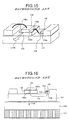
- Fig. 15 is a perspective view of a schematic configuration of a conventional semiconductor laser device.
- a submount 102 formed by AlN having an insulating characteristic and a high heat conductivity is formed on a carrier 101 formed by CuW and a semiconductor laser element 103 for outputting a laser beam L100 having a predetermined wavelength is formed on the submount 102.
- a submount 104 formed by AlN is formed on the carrier 101 and a thermistor 105 for measuring tile temperature of a semiconductor laser element is formed on the submount 104.
- the semiconductor laser element 103 and the submount 102 are joined through a metallic thin film 102a.
- the metallic thin film 102a is metallized with Ti, Pt, and Au at film thicknesses of 60, 200, and 600 nm in order and the semiconductor laser element 103 and submount 102 are joined to each other by a solder material made of AuSn or the like metallized on the Au film.
- the thermistor 105 and submount 104 are joined each other similarly through the metallic thin film 104a.
- the face to be joined with the submount 102 serves as a p-side electrode and the upper face serves as an n-side electrode and an active layer for mainly generating heat is set nearby the submount 102.
- a negative electrode is led to the n-side electrode by an Au wire 106a and the p-side electrode is led to the positive side carrier 101 through the metallic thin film 102a and an Au wire 106b.
- the submount 102 secures the insulation of the semiconductor laser element 103 and functions as a heat sink of the semiconductor laser element 103 and is joined to a CuW base 106 to be joined to the bottom of the carrier 101 by AuSn solder, and a Peltier module 107 set to the bottom of the base controls the temperature of the semiconductor laser element 103 in accordance with the temperature detected by the thermistor 105.
- the thermistor 105 is also insulated from the carrier 101 by the submount 104 similarly to the case of the semiconductor laser element 103 to detect the temperature of the semiconductor laser element 103 throuch the submount 102, carrier 101, and submount 104 respectively having a high heat conductivity.
- a conventional embodiment has a semiconductor laser element for oscillating and outputting a laser beam of 250 mW or more as a laser beam for Erbium doped fiber amplifier (EDFA) excitation.
- EDFA Erbium doped fiber amplifier
- a conventional semiconductor laser device using the above high output semiconductor laser element has a problem in that the optical output and service life of the semiconductor laser element are deteriorated.
- Fig. 16 shows a front view of the above conventional semiconductor laser device including the above described base and Peltier module.
- the submounts 102 and 104 are separately provided for the semiconductor laser element 103 and the thermistor 105.
- the heat generated in the semiconductor laser element 103 is conducted to the thermistor 105 through the metallic thin film 102a, submount 102, metallic thin film 102b, carrier 101, metallic thin film 104b, submount 104, and metallic thin film 104a in order as shown by the arrow YA in Fig. 16.
- the heat conducting distance is physically increased as described above, detection of the actual temperature of the semiconductor laser element 103 is delayed.
- the thermistor 105 detects a lower temperature having a large difference from the actual temperature of the semiconductor laser element 103 and therefore, the accuracy of a detected temperature is deteriorated.
- the temperature control of the semiconductor laser element 103 performed in accordance with the temperature detected by the thermistor 105 is delayed and because the temperature control at a low accuracy is inevitably performed, the oscillation wavelength of the semiconductor laser element 103 becomes unstable and the optical output and service life of the semiconductor laser element 103 are deteriorated.
- the total of four junction faces such as two junction faces corresponding to the metallic thin films 102a and 102b, the junction face between the carrier 101 and the base 106, and the junction face between the base 106 and the Peltier module 107 are present on the heat conducting path between the semiconductor laser element 103 and the Peltier module 107, the heating action or cooling action by the Peltier module 107 is deteriorated whenever passing through these junction faces and resultantly, the temperature control of the semiconductor laser element 103 cannot be quickly or accurately performed.
- the inter-electrode voltage of a semiconductor laser element is approximately 2 V when a current of 1 A is supplied to the semiconductor laser element, the voltage drop of the semiconductor laser element in the resonator length direction becomes un-uniform by 0.12 V That is, also when considering a current injection path, current injection into a semiconductor laser element becomes ununiform because of passing through a metallic thin film and resultantly, the light density in the active layer becomes ununiform and it is estimated to accelerate the deterioration of the optical output and service life of the semiconductor laser element.
- the first aspect of the present invention includes a semiconductor laser device including a semiconductor laser element for outputting a laser beam, a temperature measuring element for measuring the temperature of the semiconductor laser element, and a carrier having an insulating characteristic and a high heat conductivity, wherein the semiconductor laser element and the temperature measuring element are joined to the carrier through a multi-layer film that includes a gold thin film and are arranged closely to each other such that the heat resistance of a heat conducting path decreases.
- the carrier may also include rods of thermally conductive material.
- the second aspect of the present invention includes a semiconductor laser device including a semiconductor laser element for outputting a laser beam, a temperature measuring element for measuring the temperature of the semiconductor laser element, a carrier having an insulating characteristic and a high heat conductivity, and a common laser and temperature measure device submount having a heat conductivity of 500 W/(m ⁇ K) or more joined to the carrier through a multi-layer film that includes a gold thin film.
- the semiconductor laser element and the temperature measuring element are each joined to the common submount via multi-layer film that includes a gold thin film and are arranged closely to each other such that the heat resistance of a heat conducting path decreases.
- the third aspect of the present invention includes a semiconductor laser device including a semiconductor laser element for outputting a laser beam, a temperature measuring element for measuring the temperature of the semiconductor laser element, an optical monitor for monitoring the output of the laser element, and a carrier having an insulating characteristic and a high heat conductivity, wherein the semiconductor laser element, the temperature measuring element and the optical monitor are joined to the carrier through a multi-layer film that includes a gold thin film and are arranged closely to one another such that the heat resistance of a heat conducting path decreases.
- the fourth aspect includes a semiconductor laser device having a semiconductor laser element for outputting a laser beam, a temperature measuring element for measuring the temperature of the semiconductor laser element, a carrier having an insulating characteristic and a high heat conductivity, and laser submount having a heat conductivity of 500 W/(m ⁇ K) or more and a joined to the carrier through a multi-layer film that includes a gold thin film.
- the temperature measuring element is joined directly to the carrier through a multi-layer film that includes a gold thin film and is arranged closely to the semiconductor laser device such that the heat resistance of a heat conducting path decreases.
- the heat resistance of the heat conducting path is decreased by using three or less junction faces located on the heat conducting path between the semiconductor laser element and the temperature measuring element and respectively formed by the multi-layer film including the gold thin film.
- the fifth aspect of the present invention includes a semiconductor laser module having the semiconductor laser device of any of the above aspects and a temperature controlling element for controlling the temperature of the semiconductor laser element in accordance with the temperature output from the temperature measuring element.
- the carrier of the semiconductor laser device is joined to the temperature controlling element and the semiconductor laser element is temperature controlled through the carrier.
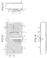
- Fig. 1A is a top view
- Fig. 1B is a front view
- Fig. 1C is a right side view of the semiconductor laser device of the first embodiment of the present invention.
- a carrier 1 is formed AlN and having an insulating characteristic and a high heat conductivity.
- a semiconductor laser element 3 outputs a laser beam having a predetermined oscillation wavelength from an end face 3a and is set to this side of a center of an upper portion of the carrier 1 through a metallic thin film 2b.
- the resonator length of the semiconductor laser element 3 is 1,000 ⁇ m or more and the semiconductor laser element 3 outputs a high output laser beam of 250 mW or more.
- the laser beam output by the semiconductor laser element 3 has an oscillation wavelength of 900 to 1,600 nm in which a 980-nm band and a 1,480-nm band are especially useful in typical communication systems and the 1,480-nm band is particularly useful as an optical fiber amplifier exciting light source such as when used as a pump for a Raman amplifier
- a thermistor 4 is set on the carrier 1 through a metallic thin film 2c, which monitors the temperature of the semiconductor laser element 3.
- Other metallic thin films 2a and 2d are formed on the carrier 1, patterned, and insulated from each other.
- the metallic thin film 2b is formed by three layers of Ti, Pt, and Au from the carrier-1 side and the three layers have thicknesses of 60, 200, and 5,000 nm. That is, in contrast to the Au film of the metallic thin film 102a shown in Fig. 15 which has a thickness of 600 nm; the Au film of the metallic thin film 2b has a thickness of 5,000 nm.
- Thickness of at least, 1,000 nm, 2,000 nm, 3,000 nm, 4,000 nm may be used as well with increasing degrees of performance and aging improvement. However, 5,000 nm is preferred.
- Other metallic thin films 2a, 2c and 2d are formed simultaneously with the metallic thin film 2b and have the same film configuration.
- the semiconductor laser element 3 is joined with the metallic thin film 2b by AuSn solder through a Pt barrier layer.
- the p-side electrode at the active layer-3b side is joined correspondingly to the carrier 1, and the n-side electrode is the upper face.
- the n-side electrode of the semiconductor laser element 3 and the metallic thin film 2a are electrically joined to each other by an Au wire 5. Therefore, the metallic thin film 2a serves as the negative electrode of the semiconductor laser element 3 and the metallic thin film 2b serves as the positive electrode of the semiconductor laser element 3.
- the n-side electrode of the semiconductor laser element 3 and the metallic thin film 2a are connected to each other by a plurality of wires 5 so that a current carrying sectional area increases. Moreover, junction points of the wires 5 are arranged at almost equal intervals to disperse power and make the current distribution more uniform.
- the width W2 of the metallic thin film 2b it is preferable to make the width W2 of the metallic thin film 2b almost equal to the width of the metallic thin film 2a. This is because the synthetic resistance value of the metallic thin films 2a and 2b is minimized when making the width W2 of the metallic thin film 2b almost equal to the width of the metallic thin film 2a. Moreover, the width W1 between the metallic thin films 2a and 2b is set to a value at which the insulation between the metallic thin films 2a and 2b can be secured.
- Bonding portions of the above wires 5 are linearly arranged in the longitudinal direction of the semiconductor laser element 3 as shown in Fig. 1. However, it is also allowed to uniformly disperse the bonding portions. In this case, it is allowed to use positions shifted from the position of the active layer 3a of the semiconductor laser element 3 as bonding portions. In short, it is an objective for the currents to be uniformly distributed on the upper face of the semiconductor laser element 3 through the wires 5.
- a conductive film or foil could be used as an alternative to the wires 5.
- the resistance of the thermistor 4 is detected by joining the bottom face of the thermistor 4 to the metallic thin film 2c and joining the upper face of the thermistor 4 to the metallic thin film 2d by a wire as illustrated and the temperature is detected by the resistance value.
- the thermistor 4 is set nearby the end face 3a from which a laser beam of the semiconductor laser element 3 is emitted.
- the end face 3a of the semiconductor laser element 3 is made almost flush with an end face of the carrier 1 so that other member does not interfere with a laser beam. otherwise the heat generated nearby the end face 3a of the semiconductor laser element 3 increases.
- the carrier 1 functions as a heat sink for the semiconductor laser element 3, the whole bottom face of the carrier 1 is joined to a CuW base 27 (Fig. 13) by AuSn solder 6, and the base 27 is joined to a Peltier module 28 (Fig. 13) for controlling the temperature of the semiconductor laser element 3.
- the Peltier module 28 prevents the semiconductor laser element 3 from being thermally saturated and the optical output and service life of the semiconductor laser element from deteriorating by mainly performing cooling correspondingly to the temperature detected by the thermistor 14 and controlling the temperature of the semiconductor laser element 3.
- the submount 102 shown in Fig. 15 (a conventional device) is not set between the semiconductor laser element 3 and the carrier 1 or the insulating submount 104 shown in Fig. 15 is not set between the thermistor 4 and the carrier 1.
- the heat conducting path between the semiconductor laser element 3 and the thermistor 4 is decreased in length at least by the thicknesses of the submounts 102 and 104 compared to the case of the conventional semiconductor laser device shown in Fig. 15.
- the thermistor 4 can quickly detect the temperature of the semiconductor laser element 3 compared to the conventional case, and temperature control could be performed more rapidly.
- the submounts 102 and 104 are excluded, two junction faces corresponding to the metallic thin films 2b and 2c are present on the heat conducting path between the semiconductor laser element 3 and the thermistor 4 the above number of junction faces is smaller than the number of junction faces (four faces) present in the conventional semiconductor laser device shown in Fig. 15. That is, in the case of the semiconductor laser device shown in Fig. 1, the heat loss is reduced at least by a value equivalent to the reduced number of junction faces compared to the conventional case and the thermistor 4 can detect a temperature closer to the actual temperature of the semiconductor laser element 3.
- the total of three junction faces such as two junction faces corresponding to the metallic thin film 2b, the junction face between the carrier 1 and the above base 27, and the junction face between the base 27 and the Peltier module 28 are present on the heat conducting path between the semiconductor laser element 3 and the Peltier module 28.
- This number is smaller than the case of the conventional semiconductor laser device described for Fig. 16 by one face. That is, it is possible to perform the temperature control of the semiconductor laser element 3 by the Peltier module 28 more quickly and accurately than ever in the conventional device of Fig. 15.
- Fig. 2 is a graph which shows the relation of the temperature difference between the semiconductor laser element 3 and the thermistor 4 to the heat generated by the semiconductor laser element 3.
- values shown by a symbol “ ⁇ ” show the relation of the temperature difference between the semiconductor laser element 3 and the thermistor 4.
- Values shown by a symbol “ ⁇ ” show the relation of the temperature difference between the semiconductor laser element 3 and the thermistor 4 in the conventional semiconductor laser device having submounts 102 and 104 formed by AlN as shown in Fig. 15.
- a structure in which the semiconductor laser element 3 and thermistor 4 are set on the carrier 1 has a smaller temperature difference and the difference increases as a calorific value increases.
- an element calorific value is 1.0 [W]
- the configuration of the first embodiment and the configuration of the conventional example shown in Fig. 15 have almost the same temperature difference of 7°C.
- the element calorific value is 3.5 [W]
- the temperature difference is 22.5°C in the case of the first embodiment and 25°C in the case of the conventional example and thus, a difference of 2.5°C occurs.
- Fig. 3 is a graph which shows relations between injection current and output power of the semiconductor laser element 3 of the first embodiment and a conventional semiconductor laser element.
- the continuous line A shows the characteristic of the semiconductor laser element 3 of this first embodiment
- the broken line shows the characteristic of the semiconductor laser element 103 of the conventional semiconductor laser device shown in Fig. 15.
- the rate of the output power increased in accordance with the increase of injection current in the case of the semiconductor laser element 3 of this first embodiment is larger than the case of the conventional semiconductor laser element 103.
- a difference is not found between output powers between the two up to approximately 200 mA of injection current.
- the output power of the conventional semiconductor laser element 103 is approximately 360 mW while the output power of the semiconductor laser element 3 of this first embodiment rises up to approximately 410 mW.
- the structure of the semiconductor laser device of this first embodiment uses the metallic thin film 2a as the conductor pattern of the n-side electrode in order to shorten wirings of the wires 5 in the above description.
- the carrier 1 through use of condtictor rods 1a embedded in the carrier 1 it is possible to eliminate the lead portion of the conductor pattern of the p-side electrode of the semiconductor laser element 3, to connect the metallic thin film 2b with a metallic thin film at the back of the carrier 1 and to supply power from the bottom side of the semiconductor laser device.
- the Au film thickness of the metallic thin film 2b is set to 5,000 ⁇ m or more so that a voltage drop due to a resistance decreases.
- a plurality of conductor rods 1 a are set to the metallic thin film 2b so that the non-uniformity of voltage drops does not occur in the resonator length direction of the semiconductor laser element 3.
- the first embodiment it is possible to prevent the optical output and service life from deteriorating even for the high output semiconductor laser element 3 because of setting the semiconductor laser element 3 and the thermistor 4 on the same carrier 1 having an insulating characteristic and a high heat conductivity, decreasing the heat conducting distance so that the thermistor 4 more quickly and accurately detects the temperature of the semiconductor laser element 3, and increasing the Au film thickness of the metallic thin film 2b formed between the semiconductor laser element 3 and the carrier 1 so as to decrease the resistance and eliminate the non-uniformity of injection currents in the resonator length direction.
- Au film thicknesses of the metallic thin films 2a to 2d are increased and the semiconductor laser element 3 and the metallic thin film 2a are connected by a plurality of wires 5. Therefore, the resistance up to the p-side and n-side electrodes of the semiconductor laser element 3 is reduced and it is possible to suppress the calorific value of the semiconductor laser device and improve the power heat conversion efficiency.
- the semiconductor laser element 3 and thermistor 4 are set on tile same carrier 1 formed by AIN.
- a semiconductor laser element 3 and a thermistor 4 are set on a submount formed by a material, such as diamond, having a heat conductivity five times larger than that of AIN.
- Fig 6A is a top view
- Fig 6B is a front view
- Fig 6C is a right side view of the semiconductor laser device of the second embodiment of the present invention.
- a carrier 13 is formed by AIN having an insulating characteristic and a high heat conductivity and a diamond submount 11 is set on the center of the upper portion through a metallic thin film 12.
- Configurations of the semiconductor laser element 3, thermistor 4, a wire 5, and metallic thin films 2a to 2d are the same as the case of the first embodiment and the same component is provided with the same symbol.
- Metallic thin films 12a to 12d corresponding to patterns of the metallic thin films 2a to 2d are formed on portions other than the area in which the diamond submount 11 is set on the carrier 13. These metallic thin films 12a to 12d are respectively formed by an Au film. That is, the metallic thin films 2a to 2d and the metallic thin films 12a to 12d are respectively bonded by the illustrated wire and each pair realizes a configuration corresponding to each of the metallic thin films 2a to 2d shown in Fig 1.
- the carrier 1 shown for the first embodiment is realized by combining the diamond submount 11 with the carrier 13.
- the total height (thickness) of the diamond submount 11 and the carrier 13 is the same as the height of the carrier 1 of the first embodiment.
- the AlN carrier 13 is held by the diamond submount 11 and base 27 in order to moderate the strain between the submount 11 and the base 27.
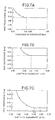
- Figs. 7A to 7C are graphs which show experiment data showing relations between sizes and heat resistances of the diamond submount 11.
- Fig. 7A is a graph which shows the relation between thicknesses and heat resistances when fixing the length of the diamond submount 11 to 2.5 mm and the width of the diamond submount to 1.0 mm.
- Fig. 7B is a graph which shows the relation between thicknesses and heat resistances when fixing the thickness of the diamond submount 11 to 0.2 mm and the width of it to 1.0 mm.
- Fig. 7C is a graph which shows the relation between widths and heat resistances when fixing the length of the diamond submount 11 to 2.5 mm and the width of it to 0.2 mm. From every graph, it is found that a heat resistance converges to a certain minimum value as a size increases. Therefore, it is possible to estimate an optimum size of the submount at which a heat resistance is minimized.
- Fig. 8 is a perspective view for explaining an optimum size of the diamond submount 11.
- the present inventor finds that it is preferable to form a diamond submount 11 at a thickness SH of 0.4 mm, a length SL of 3.2 mm, and a width SW of 3.2 mm.
- the above experiment data is a result of setting the thickness LH of the semiconductor laser element 3 to 0.13 mm, the length LL of it to 2.0 mm, and the width LW of it to 0.35 mm.
- the thickness SH For the size of the diamond submount 11, it is also possible to set the thickness SH to 0.3 mm, the length SL to 2.7 mm, and the width SW to 1.0 mm and use a structure suppressing a heat resistance within a value 1.2 times larger than the above minimum heat resistance.
- the diamond submount 11 uses polycrystal diamond synthesized through chemical vapor deposition (CVD). Diamond is a material having a highest heat conductivity, which can further improve the radiation effect of the semiconductor laser element 3.
- the whole bottom face of the carrier 13 is joined to the CuW base 27 by AuSn solder 6 and moreover, the base 27 is joined to a Peltier module 28 (Fig. 13) for controlling the temperature of the semiconductor laser element 3.
- the Peltier module 28 mainly performs cooling in accordance with the temperature detected by the thermistor 4, prevents the semiconductor laser element 3 from being thermally saturated by controlling the temperature of the semiconductor laser element 3, and prevents the optical output and the service life of the semiconductor laser element 3 from deteriorating.
- the heat conducting path between the semiconductor laser element 3 and the thermistor 4 is shortened similar to the case of the first embodiment.
- the thermistor 4 can detect the temperature of the semiconductor laser element 3 more quickly than in the first embodiment.
- the thermistor 4 can detect a temperature closer to the actual temperature of the semiconductor laser element 3. Also, it is still possible to perform the temperature control of the semiconductor laser element 3 by the Peltier module 28 (Fig. 13) more quickly and accurately than the conventional semiconductor laser device shown in Fig.
- the diamond submount 11 has a heat conductivity higher than that of AlN which is the material of a submount 102 (Fig. 15) in a conventional semiconductor laser device. Moreover, by using the diamond submount 11, it is possible to quickly diffuse the heat generated in the semiconductor laser element 3 particularly in a wide range including the transverse direction and improve the radiation effect compared to the case of a conventional AlN submount. That is, it is possible to suppress a temperature rise to an injection current compared to the case of a semiconductor laser element set to a conventional semiconductor laser device and realize a high output semiconductor laser device by resultantly converting the value equivalent to the reduction of the temperature rise into output power.
- the second embodiment it is possible to prevent the optical output and service life from deteriorating even for the high output semiconductor laser element 3. This is due to setting the semiconductor laser element 3 and thermistor 4 on the same diamond mount 11 having an insulating characteristic and a high heat conductivity and decreasing the heat conducting distance. With this configuration, the thermistor 4 more quickly and accurately detects the temperature of the semiconductor laser element 3, the resistance is decreased by increasing the Au-film thickness of the metallic thin film 2b formed between the semiconductor laser element 3 and the diamond submount 11, and the non-uniformity of current injection in the resonator length direction is eliminated.
- the semiconductor laser element 3 and thermistor 4 are set on the same substrate of the AlN carrier 1 or diamond submount 11.
- other material for the carrier such as Si or cubic boron nitride (cBN) polycrystal, having an insulating characteristic and a high heat conductivity in accordance with the thermal expansion coefficient of the semiconductor laser element 3.
- the semiconductor laser element 3 and thermistor 4 are set on a common carrier 1 or diamond submount 11.
- an optical monitor for monitoring a laser beam output from the semiconductor laser element 3 is further set on the same carrier 1 or diamond submount 11.
- Fig 9A is a top view
- Fig 9B is a front view
- Fig 9C is a left side view of the semiconductor laser device of the third embodiment of the present invention.
- the semiconductor laser device has a semiconductor laser element 3 and a thermistor 4 on a carrier 1 formed by AlN having an insulating characteristic and a high heat conductivity and moreover includes an optical monitor 7 for monitoring a laser beam radiated from the rear side of the semiconductor laser element 3.
- the optical monitor 7 is realized by a photodiode.
- the carrier 1 is provided with a conductor rod 1a to connect a metallic thin film 2e at the upper portion with AuSn solder 6 at the lower portion by a low resistance.
- the n-side electrode of the semiconductor laser element 3 is connected to a metallic thin film 2a by a wire 5a while the p-side electrode of the semiconductor laser element 3 is electrically joined with metallic thin films 2b and 2e by a wire 5b and moreover connected to the AuSn solder 6 through the conductor rod 1a and a base 27 (Fig 13).
- One electrode of the thermistor 4 is connected to a metallic thin film 2d through a wire 5d and the other electrode is connected to a metallic thin film 2c.
- One electrode of the optical monitor 7 is connected to a metallic thin film 2f through a wire 5c and the other electrode of it is connected to a metallic thin film 2g.
- the metallic thin films 2a to 2g are electrically insulated from each other.
- the metallic thin films 2a to 2g are respectively formed by three layers of Ti, Pt, and Au and have thicknesses of 60, 200, and 5,000 nm.
- the bottom face of the carrier 1 is joined to a CuW base 27 by the AuSn solder 6 and the base 27 is joined to a Peltier module 28 (Fig. 13) for controlling the temperature of the semiconductor laser element 3.
- the Peltier module 28 mainly operates in accordance with the temperature detected by the thermistor 4 and prevents the semiconductor laser element 3 from being thermally saturated and the optical output and service life of the semiconductor laser element 3 from deteriorating by controlling the temperature of the semiconductor laser element 3.
- the thickness of the Au film of the metallic thin film 2b is 5,000 nm or more, the resistance of the metallic thin film 2b decreases, the voltage drop decreases, and when a large current is injected into the semiconductor laser element 3, it is possible to decrease the non-uniformity of voltage drops in the resonator length direction of the semiconductor laser element 3 and resultantly, the optical output is prevented from deteriorating.
- the length of the heat conducting path between the semiconductor laser element 3 and thermistor 4 decreases similarly to the case of the first embodiment because the semiconductor laser element 3 and thermistor 4 are set on the carrier 1 without using the submounts 102 and 104 shown in Fig. 15.
- the thermistor 4 can quickly detect the temperature of the semiconductor laser element 3 compared to a conventional thermistor.
- decrease of heat loss due to decrease of the number of junction faces that is, the fact that the thermistor 4 can detect a temperature closer to the actual temperature of the semiconductor laser element 3 is the same as the case of the first embodiment.
- An advantage of the third embodiment is that it is possible to downsize the semiconductor laser device by setting the optical monitor on the same carrier 1.
- the optical monitor 7 is further set, the heat conducting distance is decreased, the thermistor 4 more quickly and accurately detects the temperature of the semiconductor laser element 3, and the thickness of the Au film of the metallic thin film 2b formed between the semiconductor laser element 3 and carrier 1 is increased so as to decrease the resistance and eliminate the non-uniformity of current injection in the resonator length direction.
- the fourth embodiment of the present invention is described below.
- an AlN submount on which a semiconductor laser element is mounted and an AlN submount on which a thermistor is mounted are set on the same carrier.
- the thermistor submount is excluded by directly mounting a thermistor on a carrier similar to the first embodiment and a semiconductor laser element is set on a diamond submount similar to the second embodiment.
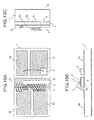
- Fig. 10A is a top view
- Fig. 10B is a front view
- Fig. 10C is a right side view of the fourth embodiment of the present invention.
- a carrier 1 is formed by AlN having a high insulating characteristic and a high heat conductivity.
- metallic thin films 2a to 2d are patterned and formed on the carrier 1 so as to be insulated from each other.
- the metallic thin films 2a to 2d are formed as a structure in which Ti, Pt, and Au are layered in order from the carrier-1 side and the layers have thicknesses of 60, 200, and 5,000 nm.
- a diamond submount 2 formed by polycrystal diamond is set on the carrier 1 through the metallic thin film 2b.
- a semiconductor laser element 3 is set on the diamond submount 2 through a metallic thin film 2h similarly to the above metallic thin film.
- the diamond submount 2 secures the insulation of the semiconductor laser element 3 and functions as a heat sink of the semiconductor laser element 3.
- the p-side electrode at the active layer side of the semiconductor laser element 3 is joined so as to face the diamond submount 2 and the n-side electrode is the upper face.
- the n-side electrode of the semiconductor laser element 3 is electrically connected with the metallic thin film 2a by Au wires 5,
- the p-side electrode and metallic thin film 2b of the semiconductor laser element 3 are electrically connected to each other through a metallic thin film 2h and an illustrated wire. Therefore, the metallic thin film 2a serves as the negative electrode of the semiconductor laser element 3 and the metallic thin film 2b serves as the positive electrode of the semiconductor laser element 3.
- the wires 5 for electrically connecting the n-side electrode with the metallic thin film 2a of the semiconductor laser element 3 are constituted by a plurality of wires so as to increase the current carrying area.
- the resistance value generated at a wiring portion decreases and it is possible to reduce the voltage drop at the portion.
- Reduction of the voltage drop contributes to suppression of heat generation and increase of a power ratio only used for a laser beam output and resultantly improves a power light conversion efficiency.
- by making intervals between connection points of the wires 5 almost equal it is possible to realize power dispersion. Thereby, it is possible to reduce the non-uniformity of voltage drops and resultantly prevent the optical output and service life of the semiconductor laser element from deteriorating.
- Bonding portions of the above wires 5 are linearly arranged in the longitudinal direction of the semiconductor laser element 3 as shown in Fig. 10A. However, it is also allowed to uniformly disperse the bonding portions on the surface of the n-side electrode of the semiconductor laser element 3. In this case, it is also possible to set the bonding portions to positions shifted from the position of the active layer of the semiconductor laser element 3. In short, it is preferable that currents are uniformly distributed on the upper face of the semiconductor laser element 3 through the wires 5.
- a thermistor 4 for measuring the temperature of the semiconductor laser element 3 is set on the carrier 1 through the metallic thin film 2c.
- the lower face of the thermistor 4 serving as one electrode is joined to the metallic thin film 2c and the upper face of it serving as the other electrode is electrically connected with the metallic thin film 2d through the illustrated wire.
- the high output semiconductor laser element 3 By setting the high output semiconductor laser element 3 so that the end face 3a of the semiconductor laser element 3 becomes almost flush with the end face of the carrier 1, it is possible to reduce the interference of a laser beam generated with other member.
- the vicinity of the end face 3a of the semiconductor laser element 3 cannot greatly receive the radiation effect by the submount 2 and therefore, the vicinity easily has a high temperature compared to other portion of the semiconductor laser element 3. Therefore, it is particularly preferable to set the thermistor 4 nearby the end face 3a from which a laser beam of the semiconductor laser element 3 is emitted.
- the length of the heat conducting path between the semiconductor laser element 3 and the thermistor 4 is decreased by at least the thickness of the excluded submount 104 compared to the case of the conventional semiconductor laser device shown in Fig. 15. Thereby, the thermistor 4 can detect the temperature of the semiconductor laser element 3 more quickly than ever.
- the heat resistance decreases by at least a value equivalent to reduction of the number of junction faces compared to a conventional case and the thermistor 4 can detect a temperature closer to the actual temperature of the semiconductor laser element 3.
- the diamond submount 2 has a heat conductivity higher than that of AlN which is the material of the conventional submount 102 shown in Fig. 15.
- the diamond submount 2 it is possible to quickly diffuse the heat generated in the semiconductor laser element 3 particularly in a wide range including the transverse direction and improve the radiation effect compared to the case of a conventional AIN submount. That is, it is possible to suppress a temperature rise to an injection current compared to the case of a semiconductor laser element set to a conventional semiconductor laser device and realize a high output semiconductor laser device.
- Fig. 11 is a graph which shows relations between injection currents and output powers of the semiconductor laser element 3 of this fourth embodiment and a conventional semiconductor laser element.
- the continuous line B shows the characteristic of the semiconductor laser element 3 of this fourth embodiment
- the broken line shows the characteristic of the semiconductor laser element 103 of the conventional semiconductor laser device shown in Fig. 15.
- the rate of the output power increasing in accordance with increase of an injection current of the semiconductor laser element 3 of this fourth embodiment is larger than that of the conventional semiconductor laser element 103.
- the output power of the semiconductor laser element 3 of this fourth embodiment rises up to approximately 440 mW while the output power of the conventional semiconductor laser element 103 is approximately 360 mW at an injection current of approximately 1,500 mA.
- the structure shown in Fig. 10 makes it possible to carry a current to the p-side electrode of the semiconductor laser element 3 by connecting the metallic thin film 2h on the diamond mount 2 with the metallic thin film 2b on the carrier 1 through a wire.
- the thin film that covers the diamond mount includes Au thin film.
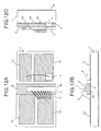
- Fig. 12A is a top view
- Fig. 12B is a front view
- Fig. 12C is a right side view of another configuration of the fourth embodiment of the present invention.
- a portion common to that in Fig. 10 is provided with the same symbol and its description is omitted.
- Figs. 12A to 12C are different from Figs. 10A to 10C in that the upper face and side face of the diamond submount 2 are covered with a metallic thin film 2i and wires for connecting the metallic thin films 2h and 2b shown in Fig. 10 each other are excluded.
- the metallic thin film 2f electrically contacts the p-side electrode of the semiconductor laser element 3 located on the upper face of the diamond submount 2 and the metallic thin film 2b on the carrier 1 to electrically connect the electrode with the metallic thin film 2b.
- the fourth embodiment has all the advantages of the second embodiment.
- the thermistor 4 is set on the carrier 1 without using a submount, production costs and complexity can be reduced compared to the second embodiment.
- Fig. 13 is a sectional view which shows a configuration of the semiconductor laser module that is the fifth embodiment of the present invention.
- the semiconductor laser module 20 has a semiconductor laser device 30 corresponding to the semiconductor laser device described for the above-described third embodiment.
- a Peltier module 28 serving as a temperature controller is set on the inside bottom face of a package 29 made of a copper tungsten alloy or the like.
- a base 27 is set on the Peltier module 28 and a carrier 34 functioning as a heat sink is set on the base 27.
- a semiconductor laser element 31, a thermistor 32, and an optical monitor 33 are arranged on the carrier 34 and the semiconductor laser device 30 corresponding to the semiconductor laser device described for the above third embodiment.
- a first lens 22 is set on the base 27.
- a laser beam emitted from the semiconductor laser element 31 is guided to an optical fiber 25 through the first lens 22, an isolator 23, and a second lens 24.
- the second lens 24 is set onto the optical fiber 25 on the optical axis of the laser beam and optically coupled with the optical fiber 25 to be externally connected.
- the optical monitor 33 monitors and detects the light leaked from the reflection film side of the semiconductor laser element 31
- the isolator 23 is set between the semiconductor laser element 22 and the optical fiber 25 so that the return light reflected from other optical component does not reenter a resonator.
- the fifth embodiment use a semiconductor laser module for directly outputting a laser beam output from the semiconductor laser element 31, it can be also applied to an optical fiber grating semiconductor laser module for wavelength selecting and outputting a laser beam output from the semiconductor laser element 31 by forming the optical fiber grating near by an end of the second lens 5 of the optical fiber 25.
- the isolator 23 is not used.
- the semiconductor laser device uses a semiconductor laser module mounting a high output semiconductor laser element and constitutes a semiconductor laser device having the same configuration as the third embodiment, it is possible to quickly and accurately perform the temperature control of the semiconductor laser element and resultantly realize a semiconductor laser module reduced in size and weight. Moreover, even if the carrier 34 serving as a heat sink is increased in size in accordance with improvement of the semiconductor laser element 31 in output, it is possible to suppress the deterioration of a power light conversion efficiency.
- the above fifth embodiment is formed into a module by using the semiconductor laser device described for the third embodiment, it is naturally possible to replace the semiconductor laser device 30 shown in Fig. 13 with the semiconductor laser device having the configuration described for each of the first, second and fourth embodiments.
- an output power larger than that of the conventional semiconductor laser device is obtained from each of the semiconductor laser devices (A and B) shown for the first and fourth embodiments.
- a largest output power of approximately 377 mW is obtained from the semiconductor laser device (B) having a structure in which only the thermistor 4 is set on the carrier 1 and the semiconductor laser element 3 is set on the diamond submount 2 and then, an output power of approximately 370 mW is obtained from the semiconductor laser device (A) in which the semiconductor laser element 3 is set on the carrier 1
- the diamond submount 2 has a very large radiation effect because a large output power is obtained from a structure (B) constituted by adding the diamond submount 2 on which the semiconductor laser element 3 is set to a structure (A) having the shortest heat conducting path compared to the case of the structure (A).
- a submount set immediately below the semiconductor laser element 3 is formed by diamond.
- the diamond having a high heat conductivity of 1,000 to 1,300 W/(m ⁇ K).
- a semiconductor laser element for outputting a laser beam and a temperature measuring element for measuring the temperature of the semiconductor laser element are arranged on the same carrier having an advantageous insulating characteristic and a high heat conductivity and the semiconductor laser element and the temperature measuring element are joined to the carrier through a specially configured multi-layer film that includes a gold thin film so as to decrease the heat resistance of a heat conducting path including proximity arrangement. Therefore, advantages are obtained that the temperature measuring element can more accurately and quickly detects the temperature of the semiconductor laser element and prevent the optical output and service life of the semiconductor laser element from deteriorating. And because the carrier is formed by any one of Si, AlN, diamond, and cBN polycrystal, or a combination of them, an advantage is obtained that it is possible to flexibly select a material of the carrier.
- a semiconductor laser element for outputting a laser beam is joined to a submount formed by a heat sink joined to a carrier and having a heat conductivity of 500 W/(m ⁇ K) or more through a multi-layer film including a gold thin film, and a temperature measuring element for measuring the temperature of the semiconductor laser element is joined, either via the same submount or directly, to the same carrier having an insulating characteristic and a high heat conductivity through a specially configured multi-layer film that includes a gold thin film so as to decrease the heat resistance of a heat conducting path including proximity arrangement. Therefore, advantages are obtained that the temperature measuring element can more accurately and quickly detect the temperature of the semiconductor laser element and prevent the optical output and service life of the semiconductor laser element from deteriorating.
- An advantage unique to the fourth aspect of the invention in the restriction of use of the submount to just semiconductor laser element is a reduction in production costs.
- a monitor element for monitoring the output of a laser beam output by a semiconductor laser element is also set on the carrier via a specially configured multi-layer film, an advantage is obtained that it is possible to further accelerate the decrease of a semiconductor laser device in size and weight. And because at least one of the semiconductor laser element, temperature measuring element, and monitor element is made electrically independent, an advantage is obtained that it is possible to further accelerate the decrease of a semiconductor laser device in size and weight.
- the semiconductor laser element and the temperature measuring element electrically join one electrode with the above conductor pattern by conductive wires and decrease lengths and the density of the wires, an advantage is obtained that it is possible to decrease the semiconductor laser device in size and weight.
- the conductive wires can be joined each other at almost equal intervals on the semiconductor laser element, and the temperature measuring element, and/or the above conductor pattern to uniform voltage drops to the semiconductor laser element and minimize voltage drops and heat generation due to the conductive wires, advantages are obtained that it is possible to prevent the optical output and service life of the semiconductor laser element from deteriorating, reduce the total heat generation of a semiconductor laser device, and improve the power light conversion efficiency of the semiconductor laser device.
- the thickness of the gold thin film is set to 5 ⁇ m or more so that the heat resistance between a semiconductor laser element and a temperature measuring element decreases and moreover, the voltage drop of the above conductor pattern is suppressed, advantages are obtained that the temperature measuring element can quickly and accurately detect the temperature of the semiconductor laser element, resultantly the temperature measuring element can quickly and accurately perform the temperature control of the semiconductor laser element and improve a power light conversion efficiency due to reduction of the voltage drop of the conductor pattern. These advantages are possible even for a high output semiconductor laser element has resonator length of 1.000 ⁇ m or more.
- the active layer side of the semiconductor laser element is joined to the carrier, the active layer for generating much heat is made to approach a carrier and a submount at a lower layer, heat sink functions of them are maximally shown, and temperature measurement is perform at a high accuracy by a temperature measuring element, advantages are obtained that it is possible to prevent the optical output of the semiconductor laser element from deteriorating and improve the reliability, particularly the service life of the semiconductor laser element. Also, because the temperature control of the semiconductor laser element can be quickly and accurately performed even if the output of a laser beam output from the semiconductor laser element is set to a high output of 250 mW or more, an advantage is obtained that it is possible to prevent the optical output from deteriorating even for a high output semiconductor laser element.
- the carrier of a semiconductor laser device is joined to a temperature controlling element such as a Peltier module, a semiconductor laser element and a temperature measuring element are arranged on the carrier, the semiconductor laser element is temperature controlled in accordance with the temperature measured by the temperature measuring element, an advantage is obtained that it is possible to realize a semiconductor laser module capable of preventing the optical output and service life from deteriorating even when the semiconductor laser element has a high output.
- a temperature controlling element such as a Peltier module
- a semiconductor laser element and a temperature measuring element are arranged on the carrier, the semiconductor laser element is temperature controlled in accordance with the temperature measured by the temperature measuring element, an advantage is obtained that it is possible to realize a semiconductor laser module capable of preventing the optical output and service life from deteriorating even when the semiconductor laser element has a high output.
- the heat resistance of the heat conducting path between the semiconductor laser element and the temperature controlling element is decreased by decreasing the number of junction faces located on the heat conducting path and respectively formed by a multi-layer film including a gold thin film to four or less.
Landscapes
- Physics & Mathematics (AREA)
- Condensed Matter Physics & Semiconductors (AREA)
- General Physics & Mathematics (AREA)
- Electromagnetism (AREA)
- Optics & Photonics (AREA)
- Semiconductor Lasers (AREA)
Abstract
Description
Claims (90)
- A semiconductor laser device comprising:a carrier configured to have an insulating characteristic and a high heat conductivity;a multi-layer film including a gold thin film mounted on the carrier;a semiconductor laser element having a p-side electrode, an n-side electrode, and an end-face, configured to emit a laser beam, and mounted on the multi-layer film via the p-side electrode; anda temperature measuring element having a first-side and a second-side. configured to measure a temperature of the semiconductor laser element, and mounted on the multi-layer film via the second-side, whereinthe semiconductor laser element and the temperature measuring element are placed in a proximity to facilitate a transfer of heat from the laser element p-side to the measuring element second-side without use of a submount.
- The semiconductor laser device according to claim 1, wherein:the carrier comprises at least one of a Si, AIN, diamond and cBN polycrystal material.
- The semiconductor laser device according to claim 2, wherein:the multi-layer film is arranged to form a electrical conducting pattern having a laser mount portion, a measuring element mount portion, a laser n-side portion, and a measuring element first-side portion:the semiconductor laser element n-side electrode is connected to the laser n-side portion via a conductive connection; andthe temperature measuring element first-side is connected to the measuring element first-side portion via an other conductive connection.
- The semiconductor laser device according to claim 3, wherein:the conductive connection comprises a plurality of conductive wires, andthe plurality of conductive wires are joined at substantially equal intervals on the laser n-side portion of the semiconductor laser element.
- The semiconductor laser device according to claim 3, wherein:the laser n-side portion is placed on a portion of the carrier closest to the laser device end-face.
- The semiconductor laser device according to claim 3. wherein:the laser n-side portion is placed on a portion of the carrier opposite to the laser device end-face.
- The semiconductor laser device according to claim 3, wherein:the carrier comprises a conductor rod with a rod thermal conductivity higher than a thermal conductivity of the carrier.
- The semiconductor laser device according to claim 1, wherein:the gold thin film is has a thickness equal to or greater than 5 µm.
- The semiconductor laser device according to claim 1, further comprising:a monitor element mounted on the carrier to monitor the laser beam.
- The semiconductor laser device according to claim 1, wherein:a resonator length of the semiconductor laser element is equal to or greater than 1,000 µm.
- The semiconductor laser device according to claim 9, wherein:at least one of the semiconductor laser element, the temperature measuring element, and the monitor element is electrically independent from an other one of semiconductor laser element, the temperature measuring element, and the monitor element.
- The semiconductor laser device according to claim 1, wherein:the semiconductor laser element is configured to output optical power at a level equal to or greater than 250 mW.
- The semiconductor laser device according to claim 3, wherein:the carrier is configured to maintain a difference between an actual laser element temperature and a measured laser element temperature less than or equal to 22.5 degrees C when the semiconductor laser element is driven so as to have a calorific value of 3.5(W).
- The semiconductor laser device according to claim 3, wherein:the carrier is configured to enable the semiconductor laser element to output at least 410 mW of optical power without saturating when injected with an injection current of 1500 mA.
- A semiconductor laser device comprising:a carrier configured to have an insulating characteristic and a high heat conductivity;a submount formed by a heat sink having a heat conductivity equal to or greater than 500 W/(m · K) and joined to the carrier through a first multi-layer film;a second multi-layer film including a gold thin film mounted on the submount;a third multi-layer film including a gold thin film mounted on the carrier;a semiconductor laser element having a p-side electrode, an n-side electrode. and an end-face, configured to emit a laser beam, and mounted on the second multi-layer film via the p-side electrode; anda temperature measuring element having a first-side and a second-side, configured to measure a temperature of the semiconductor laser element, and mounted on the second multi-layer film via the second-side, whereinthe semiconductor laser element and the temperature measuring element are placed in a proximity to facilitate a transfer of heat from the laser element p-side to the measuring element second-side.
- The semiconductor laser device according to claim 15, wherein:the submount comprises diamond.
- The semiconductor laser device according to claim 16, wherein:the second multi-layer film is configured to form a conductor pattern having a laser mount portion, a measuring element mount portion, a laser n-side portion, and a measuring element first-side portion.the third multi-layer film is arranged to form a electrical conducting pattern having an other laser mount portion, an other measuring element mount portion, an other laser n-side portion, and an other measuring element first-side portion,the semiconductor laser element n-side electrode is connected to the laser n-side portion via a first conductive connection.the laser mount portion is connected to the other laser mount portion via a second conductive connection,the laser n-side portion is connected to the other laser n-side portion via a third conductive connection.the temperature measuring element first-side is connected to the measuring element first-side portion via a fourth conductive connection,the measuring element first-side portion is connected to the other measuring element first-side portion via a fifth conductive connection, andthe measuring element mount portion is connected to the other measuring element mount portion via a sixth conductive connection.
- The semiconductor laser device according to claim 17, wherein:the first conductive correction, second conductive correction and third conductive connection comprises a respective first plurality, second plurality and third plurality of conductive wires,the first plurality, second plurality and third plurality of conductive wires are each configured to be joined at substantially equal intervals on the respective semiconductor laser element n-side electrode, the laser n-side portion, and other laser n-side portion.
- The semiconductor laser device according to claim 17, wherein:the laser n-side portion is placed on a portion of the carrier closest to the laser device end-face.
- The semiconductor laser device according to claim 17, wherein:the laser n-side portion is placed on a portion of the carrier opposite to the laser device end-face.
- The semiconductor laser device according to claim 15, wherein:the gold thin film has a thickness equal to or greater than 5 µm.
- The semiconductor laser device according to claim 15, further comprising:a monitor element mounted on the carrier to monitor the laser beam.
- The semiconductor laser device according to claim 15, wherein:a resonator length of the semiconductor laser element is equal to or greater than 1,000 µm.
- The semiconductor laser device according to claim 22, wherein:at least one of the semiconductor laser element, the temperature measuring element, and the monitor element is electrically independent from an other one of semiconductor laser element, the temperature measuring element, and the monitor element.
- The semiconductor laser device according to claim 15, wherein:the semiconductor laser element is configured to have an output power equal to or greater than 250 mW.
- The semiconductor laser device according to claim 16, wherein:the diamond submount is configured to minimize heat resistance relative to a semiconductor laser element length, width and thickness.
- The semiconductor laser device according to claim 26, wherein:the diamond submount has a thickness of at least 0.4 mm, a length of at least 3.2 mm and a width of at least 3.2 mm when the semiconductor laser element has a thickness of not more than 0.13 mm, a length of not more than 2.0 mm and a width of not more than 0.35 mm
- The semiconductor laser device according to claim 26, wherein:the diamond submount has a thickness of at least 0.3 mm, a length of at least 2.7 mm and a width of at least 1.0 mm when the semiconductor laser element has a thickness of not more than 0.13 mm, a length of not more than 2.0 mm and a width of not more than 0.35 mm
- The semiconductor laser device according to claim 16, wherein:the diamond submount comprises a polycrystal diamond.
- A semiconductor laser device comprising:a carrier configured to have an insulating characteristic, a high heat conductivity and a conductor rod with a rod thermal conductivity higher than a thermal conductivity of the carrier;a multi-layer film including a gold thin film mounted on the carrier;a semiconductor laser element having a p-side electrode, an n-side electrode, and an end-face, configured to emit a laser beam, and mounted on the multi-layer film via the p-side electrode:a temperature measuring element having a temperature measuring element first-side and a temperature measuring element second-side, configured to measure a driving temperature of the semiconductor laser element, and mounted on the multi-layer film via the temperature measuring element second-side; anda laser monitoring element having a laser monitoring element first-side and a laser monitoring element second-side, configured to monitor the laser beam, and mounted on the multi-layer film via the laser monitoring element second-side, whereinthe semiconductor laser element and the temperature measuring element are placed in a proximity to facilitate a transfer of heat from the laser element p-side to the measuring element second-side.
- The semiconductor laser device according to claim 30, wherein:the carrier comprises at least one of a Si, AlN, diamond and cBN polycrystal material.
- The semiconductor laser device according to claim 31, wherein:the multi-layer film is arranged to form a electrical conducting pattern having a laser mount portion, a measuring element mount portion. a laser monitoring element mount portion, a laser n-side portion, a measuring element first-side portion, and a laser monitoring element first-side portion, whereinthe semiconductor laser element n-side electrode is connected to the laser n-side portion via a first conductive connection,the temperature measuring element first-side is connected to the measuring element first-side portion via a second conductive connection, andthe laser monitoring element first-side is connected to the laser monitoring element first-side portion via a third conductive connection.
- The semiconductor laser device according to claim 32, wherein:the first conductive connection comprises a plurality of conductive wires; andthe plurality of conductive wires are joined at substantially equal intervals on the laser n-side portion of the semiconductor laser element.
- The semiconductor laser device according to claim 32, wherein:the laser n-side portion is placed on a portion of the carrier closest to the laser device end-face.
- The semiconductor laser device according to claim 32, wherein:the laser n-side portion is placed on a portion of the carrier opposite to the laser device end-face.
- The semiconductor laser device according to claim 30. wherein:the gold thin film has a thickness equal to or greater than 5 µm.
- The semiconductor laser device according to claim 30, further comprising:a diamond submount interposed between the carrier and the semiconductor laser element, the temperature measure element and the laser monitoring element, whereinthe diamond submount is joined to the carrier by a multi-layer film including a gold thin film, andthe semiconductor laser element, the temperature measure element and the laser monitoring element are each joined to the diamond submount by a multi-layer film including a gold thin film.
- The semiconductor laser device according to claim 30, wherein:a resonator length of the semiconductor laser element is equal to or greater than 1,000 µm.
- The semiconductor laser device according to claim 37, wherein:at least one of the semiconductor laser element, the temperature measuring element, and the monitor element is electrically independent from an other one of semiconductor laser element, the temperature measuring element, and the monitor element.
- The semiconductor laser device according to claim 30, wherein:the semiconductor laser element is configured to have an output power equal to or greater than 250 mW.
- A semiconductor laser device comprising:a carrier configured to have an insulating characteristic and a high heat conductivity;a submount formed by a heat sink having a heat conductivity equal to or greater than 500 W/(m · K) and joined to the carrier through a first multi-layer film;a second multi-layer film including a gold thin film mounted on the submount;a third multi-layer film including a gold thin film mounted on the carrier;a semiconductor laser element having a p-side electrode, an n-side electrode. and an end-face, configured to emit a laser beam, and mounted on the second multi-layer film via the p-side electrode; anda temperature measuring element having a first-side and a second-side, configured to measure a temperature of the semiconductor laser element, and mounted on the third multi-layer film via the second-side, whereinthe semiconductor laser element and the temperature measuring element are placed in a proximity to facilitate a transfer of heat from the laser element p-side to the measuring element second-side.
- The semiconductor laser device according to claim 41, wherein:the submount comprises a diamond.
- The semiconductor laser device according to claim 42, wherein:the second multi-layer film is configured to form a conductor pattern having a laser mount portion; andthe third multi-layer film is arranged in a pattern to conduct heat and having an other laser mount portion, a measuring element mount portion, a laser n-side portion, and a measuring element first-side portion, whereinthe semiconductor laser element n-side electrode is connected to the laser n-side portion via a first conductive connection,the laser mount portion is connected to the other laser mount portion via a second conductive connection, andthe temperature measuring element first-side is connected to the measuring element first-side portion via a third conductive connection.
- The semiconductor laser device according to claim 43, wherein:the first conductive connection and second conductive connection comprises a respective first plurality and second plurality of conductive wires.the first plurality and second plurality of conductive wires are each configured to be joined at substantially equal intervals on the respective scmiconductur laser element n-side electrode, the laser n-side portion, and other laser n-side portion.
- The semiconductor laser device according to claim 41, wherein:the gold thin film has a thickness equal to or greater than 5 µm.
- The semiconductor laser device according to claim 41, further comprising:a monitor element mounted on the carrier to monitor the laser beam.
- The semiconductor laser device according to claim 41, wherein:a resonator length of the semiconductor laser element is equal to or greater than 1,000 µm.
- The semiconductor laser device according to claim 46, wherein:at least one of the semiconductor laser element, the temperature measuring element, and the monitor element is electrically independent from an other one of semiconductor laser element, the temperature measuring element, and the monitor element.
- The semiconductor laser device according to claim 41, wherein:the semiconductor laser element is configured to have an output power equal to or greater than 250 mW.
- The semiconductor laser device according to claim 43, whereinthe carrier is configured to enable the semiconductor laser element to output essentially 440 mW of power without saturating when injected with an injection current of 1500 mA.
- A semiconductor laser device comprising:a carrier configured to have an insulating characteristic and a high heat conductivity;a diamond submount covered with a metallic thin film and joined to the carrier through a first multi-layer film;a second multi-layer film including a gold thin film mounted on the submount;a third multi-layer film including a gold thin film mounted on the carrier;a semiconductor laser element configured to emit a laser beam, mounted on the second multi-layer film via the p-side electrode, and having a p-side electrode, an n-side electrode, and an end-face; anda temperature measuring element having a first-side and a second-side, configured to measure a temperature of the semiconductor laser element, and mounted on the third multi-layer film via the second-side, whereinthe semiconductor laser element and the temperature measuring element are placed in a proximity to facilitate a transfer of heat from the laser element p-side to the measuring element second-side.
- The semiconductor laser device according to claim 51, wherein:the second multi-layer film is configured to form a conductor pattern having a laser mount portion;the third multi-layer film is configured to form a conductor pattern having a measuring element mount portion, a laser n-side portion, at least one of a laser p-side portion and a sub-mount mount portion, and a measuring element first-side portion;the semiconductor laser element n-side electrode is connected to the laser n-side portion via a first conductive connection; andthe temperature measuring element first-side connects to the measuring element first-side portion via a second conductive connection.
- The semiconductor laser device according to claim 52, wherein:the first conductive connection comprises a plurality of conductive wires; andthe plurality of conductive wires arc each configured to be joined at essentially equal intervals on the respective semiconductor laser element n-side electrode and the laser n-side portion.
- The semiconductor laser device according to claim 51, wherein:the gold thin film has a thickness equal to or greater than 5 µm.
- The semiconductor laser device according to claim 51, further comprising:a monitor element mounted on the carrier to monitor the laser beam.
- The semiconductor laser device according to claim 1, wherein:a resonator length of the semiconductor laser element is equal to or greater than 1,000 µm.
- The semiconductor laser device according to claim 55, wherein:at least one of the semiconductor laser element, the temperature measuring element, and the monitor element is electrically independent from an other one of semiconductor laser element, the temperature measuring element, and the monitor element.
- The semiconductor laser device according to claim 51, wherein:the semiconductor laser element is configured to have an output power equal to or greater than 250 mW.
- A semiconductor laser module, comprising:a first lens mounted on the base:a laser housing having a housing floor;a peltier module mounted on the housing floor;a base mounted on the peltier module:a semiconductor laser device mounted on the base and having
a carrier configured to have an insulating characteristic and a high heat conductivity.
a multi-layer film including a gold thin film mounted on the carrier,
a semiconductor laser element having a p-side electrode, an n-side electrode, and an end-face, configured to emit a laser beam, and mounted on the multi-layer film via the p-side electrode, and
a temperature measuring element having a first-side and a s econd-side, configured to measure a temperature of the semiconductor laser element, and mounted on the multi-layer film via the second-side, wherein
the semiconductor laser element and the temperature measuring element are placed in a proximity to facilitate a transfer of heat from the laser element p-side to the measuring element second-side without use of a submount;an isolator and a second lens mounted in the package; andan optical fiber. - The semiconductor laser module according to claim 59, wherein:the carrier comprises at least one of a Si, AIN, diamond and cBN polycrystal material.
- The semiconductor laser module according to claim 60, wherein:the multi-layer film is arranged to form a conductor pattern having a laser mount portion, a measuring element mount portion, a laser n-side portion, and a measuring element first-side portion;the semiconductor laser element n-side electrode connects to the laser n-side portion via a conductive connection; andthe temperature measuring element first-side connects to the measuring element first-side portion via an other conductive connection.
- A semiconductor laser module, comprising:a laser housing having a housing floor;a peltier module mounted on the housing floor:a base mounted on the peltier module;a semiconductor laser device mounted on the base and having
a carrier configured to have an insulating characteristic and a high heat conductivity.
a submount formed by a heat sink having a heat conductivity equalto or greater than 500 W/(m · K) and joined to the carrier through a first multi-layer film.
a second multi-layer film including a gold thin film mounted on the submount,
a third multi-layer film including a gold thin film mounted on the carrier,
a semiconductor laser element having a p-side electrode, an n-side electrode, and an end-face, configured to emit a laser beam, and mounted on
the second multi-layer film via the p-side electrode, and
a temperature measuring element having a first-side and a second-side, configured to measure a temperature of the semiconductor laser element, and mounted on the second multi-layer film via the second-side,
wherein
the semiconductor laser element and the temperature measuring element are placed in a proximity to facilitate a transfer of heat from the laser element p-side to the measuring element second-side;
a first lens mounted on the base;
an isolator and a second lens mounted in the package; and
an optical fiber. - The semiconductor laser module according to claim 62, wherein:the submount comprises a diamond.
- The semiconductor laser module according to claim 63, wherein:the second multi-layer film is arranged to form a conductor pattern having a laser mount portion, a measuring element mount portion, a laser n-side portion, and a measuring element first-side portion;the third multi-layer film is configured to form a conductor pattern having an other laser mount portion, an other measuring element mount portion, an other laser n-side portion, and an other measuring element first-side portion.the semiconductor laser element n-side electrode connects to the laser n-side portion via a first conductive connection;the laser mount portion connects to the other laser mount portion via a second conductive connection;the laser n-side portion connects to the other laser n-side portion via a third conductive connection;the temperature measuring element first-side connects to the measuring element first-side portion via a fourth conductive connection;the measuring element first-side portion connects to the other measuring element first-side portion via a fifth conductive connection; andthe measuring element mount portion connects to the other measuring element mount portion via a sixth conductive connection.
- A semiconductor laser module, comprising:a laser housing having a housing floor;a peltier module mounted on the housing floor;a base mounted on the peltier module;a semiconductor laser device mounted on the base and having
a carrier configured to have an insulating characteristic, a high heat conductivity and a conductor rod configured to have a rod thermal conductivity higher than a thermal conductivity of the carrier,
a multi-layer film including a gold thin film mounted on the carrier,
a semiconductor laser element having a p-side electrode, an n-side electrode, and an end-face, configured to emit a laser beam, and mounted on the multi-layer film via the p-side electrode,
a temperature measuring element having a temperature measuring element first-side and a temperature measuring element second-side, configured to measure a temperature of the semiconductor laser element, and mounted on the multi-layer film via the temperature measuring element second-side, and
a laser monitoring element having a laser monitoring element first-side and a laser monitoring element second-side, configured to monitor the laser beam, and mounted on the multi-layer film via the laser monitoring element second-side, wherein
the semiconductor laser element and the temperature measuring element are placed in a proximity to facilitate a transfer of heat from the laser element p-side to the measuring element second-side without a submount:a first lens mounted on the base;an isolator and a second lens mounted in the package; andan optical fiber. - The semiconductor laser module according to claim 65, wherein:the carrier comprises at least one of a Si, AlN, diamond and cBN polycrystal material.
- The semiconductor laser module according to claim 66, wherein:the multi-layer film is arranged to form a conductor pattern having a laser mount portion, a measuring element mount portion, a laser monitoring element mount portion, a laser n-side portion, a measuring element first-side portion and, a laser monitoring element first-side portion;the semiconductor laser element n-side electrode connects to the laser n-side portion via a first conductive connection;the temperature measuring element first-side connects to the measuring element first-side portion via a second conductive connection; andthe laser monitoring element first-side connects to the laser monitoring element first-side portion via a third conductive connection.
- A semiconductor laser module, comprising:a laser housing having a housing floor;a peltier module mounted on the housing floor;a base mounted on the peltier module;a semiconductor laser device mounted on the base and having
a carrier configured to have an insulating characteristic and a high heat conductivity,
a submount formed by a heat sink having a heat conductivity equal to or greater than 500 W/(m · K) and joined to the carrier through a first multi-layer film,
a second multi-layer film including a gold thin film mounted on the submount,
a third multi-layer film including a gold thin film mounted on the carrier,
a semiconductor laser element having a p-side electrode, an n-side electrode, and an end-face, configured to emit a laser beam, and mounted on the second multi-layer film via the p-side electrode, and
a temperature measuring element having a first-side and a second-side, configured to measure a temperature of the semiconductor laser element, and mounted on the third multi-layer film via the second-side, wherein
the semiconductor laser element and the temperature measuring element are placed in a proximity to facilitate a transfer of heat from the laser element p-side to the measuring element second-side;
a first lens mounted on the base;
an isolator and a second lens mounted in the package; and
an optical fiber. - The semiconductor laser module according to claim 68, wherein:the submount comprises a diamond.
- The semiconductor laser module according to claim 69, wherein:the second multi-layer film is arranged to form a conductor pattern having a laser mount portion;the third multi-layer film is configured to form a conductor pattern having an other laser mount portion, a measuring element mount portion, a laser n-side portion, and a measuring element first-side portion;the semiconductor laser element n-side electrode connects to the laser n-side portion via a first conductive connection;the laser mount portion connects to the other laser mount portion via a second conductive connection; andthe temperature measuring element first-side connects to the measuring element first-side portion via a third conductive connection.
- A semiconductor laser module, comprising:a laser housing having a housing floor;a peltier module mounted on the housing floor;a base mounted on the peltier module;a semiconductor laser device mounted on the base and having
a carrier configured to have an insulating characteristic and a high heat conductivity,
a diamond submount covered with a metallic thin film and joined to the carrier through a first multi-layer film,
a second multi-layer film including a gold thin film mounted on the submount,
a third multi-layer film including a gold thin film mounted on the carrier,
a semiconductor laser element configured to emit a laser beam, mounted on the second multi-layer film via the p-side electrode, and having a p-side electrode, an n-side electrode, and an end-face, and
a temperature measuring element having a first-side and a second-side, configured to measure a temperature of the semiconductor laser element, and mounted on the third multi-layer film via the second-side, wherein
the semiconductor laser element and the temperature measuring element are placed in a proximity to facilitate a transfer of heat from the laser element p-side to the measuring element second-side;
a first lens mounted on the base;
an isolator and a second lens mounted in the package; and
an optical fiber. - The semiconductor laser module according to claim 71, wherein:the second multi-layer film is configured to form a conductor pattern having a laser mount portion;the third multi-layer film is configured to form a conductor pattern having a measuring element mount portion, a laser n-side portion, at least one of a laser p-side portion and a sub-mount mount portion, and a measuring element first-side portion, the semiconductor laser element n-side electrode connects to the laser n-side portion via a first conductive connection; andthe temperature measuring element first-side connects to the measuring element first-side de portion via a second conductive connection.
- A semiconductor laser device comprising:a carrier configured to have an insulating characteristic and a high heat conductivity;a first and a second multi-layer film including a gold thin film mounted on the carrier;a semiconductor laser element mounted on the first multi-layer film;a temperature measuring element mounted on the second multi-layer film;means for emitting a laser beam; andmeans for measuring and controlling a temperature of the semiconductor laser element, whereina number of thermal interfaces between the semiconductor laser element and temperature measuring element is one of two and three.
- The semiconductor laser device according to claim 73, wherein:the carrier comprises at least one of a Si, AIN, diamond and cBN polycrystal material.
- The semiconductor laser device according to claim 74, wherein:the carrier comprises a thermal conducting rod having a rod thermal conductivity higher than a thermal conductivity of the carrier.
- The semiconductor laser device according to claim 74, further comprising:a common submount formed by a heat sink having a heal conductivity equal to or greater than 500 W/(m · K) interposed between the semiconductor laser element and the first multi-layer film and between the temperature monitoring device and the second multi-layer film.
- The semiconductor laser device according to claim 76, wherein:the common submount comprises a diamond.
- The semiconductor laser device according to claim 74, further comprising:an optical monitor mounted on the carrier via an optical carrier metallic film.
- The semiconductor laser device according to claim 74, further comprising:a submount formed by a heat sink having a heat conductivity equal to or greater than 500 W/(m · K) interposed between the semiconductor laser element and the first multi-layer film.
- The semiconductor laser device according to claim 79. wherein:the submount comprises a diamond.
- The semiconductor laser device according to claim 80, wherein:the submount is covered with a metallic thin film.
- A semiconductor laser module, comprising:a laser housing having a housing floor;a peltier module mounted on the housing floor;a base mounted on the peltier module;a semiconductor laser device mounted on the base and having
a carrier configured to have an insulating characteristic and a high heat conductivity,
a first and a second multi-layer film including a gold thin film mounted on the carrier.
a semiconductor laser element mounted on the first multi-layer film,
a temperature measuring element mounted on the second multi-layer film, wherein
a number of thermal interfaces between the semiconductor laser element and temperature measuring element is one of two and three;
a first lens mounted on the base;
an isolator and a second lens mounted in the package;
an optical fiber;
means for emitting a laser beam;
means for measuring and controlling a temperature of the semiconductor laser element; and
means for using a measured temperature to control an output power of the semiconductor laser element. - The semiconductor laser module according to claim 81, wherein:the carrier comprises at least one of a Si, AIN, diamond and cBN polycrystal material.
- The semiconductor laser module according to claim 82, wherein:the carrier comprises a thermal conducting rod having a rod thermal conductivity higher than a thermal conductivity of the carrier.
- The semiconductor laser module according to claim 82, further comprising:a common submount formed by a heat sink having a heat conductivity equal to or greater than 500 W/(m · K) interposed between the semiconductor laser element and the first multi-layer film and between the temperature monitoring device and the second multi-layer film.
- The semiconductor laser module according to claim 85, wherein:the common submount comprises a diamond.
- The semiconductor laser module according to claim 82, further comprising:an optical monitor mounted on the carrier via an optical carrier metallic film.
- The semiconductor laser module according to claim 82, further comprising:a submount formed by a heat sink having a heat conductivity equal to or greater than 500 W/(m · K) interposed between the semiconductor laser element and the first multi-layer film.
- The semiconductor laser module according to claim 88, wherein:the submount comprises a diamond.
- The semiconductor laser module according to claim 89, wherein:the submount is covered with a metallic thin film.
Applications Claiming Priority (4)
| Application Number | Priority Date | Filing Date | Title |
|---|---|---|---|
| JP2001059325 | 2001-03-02 | ||
| JP2001059325 | 2001-03-02 | ||
| JP2001319847 | 2001-10-17 | ||
| JP2001319847 | 2001-10-17 |
Publications (2)
| Publication Number | Publication Date |
|---|---|
| EP1239561A2 true EP1239561A2 (en) | 2002-09-11 |
| EP1239561A3 EP1239561A3 (en) | 2004-09-29 |
Family
ID=26610593
Family Applications (1)
| Application Number | Title | Priority Date | Filing Date |
|---|---|---|---|
| EP02004343A Withdrawn EP1239561A3 (en) | 2001-03-02 | 2002-03-01 | Semiconductor laser device and semiconductor laser module |
Country Status (3)
| Country | Link |
|---|---|
| US (1) | US6810049B2 (en) |
| EP (1) | EP1239561A3 (en) |
| CA (1) | CA2374334A1 (en) |
Cited By (1)
| Publication number | Priority date | Publication date | Assignee | Title |
|---|---|---|---|---|
| CN106300005A (en) * | 2016-08-29 | 2017-01-04 | 北京图来激光科技有限公司 | A kind of ceramic package device of semiconductor laser |
Families Citing this family (13)
| Publication number | Priority date | Publication date | Assignee | Title |
|---|---|---|---|---|
| US6760352B2 (en) * | 2001-09-19 | 2004-07-06 | The Furukawa Electric Co., Ltd. | Semiconductor laser device with a diffraction grating and semiconductor laser module |
| US6967982B2 (en) * | 2001-12-25 | 2005-11-22 | The Furukawa Electric Co., Ltd. | Semiconductor laser device with a strain reduction cushion function, semiconductor laser module, and semiconductor laser device fabrication method |
| DE10258745A1 (en) * | 2002-12-13 | 2004-07-08 | Hentze-Lissotschenko Patentverwaltungs Gmbh & Co.Kg | Semiconductor laser device, semiconductor laser module for such a semiconductor laser device and a method for producing such a semiconductor laser device |
| JP4072093B2 (en) * | 2003-05-20 | 2008-04-02 | 株式会社日立製作所 | Semiconductor laser module |
| DE102004014207A1 (en) * | 2004-03-23 | 2005-10-13 | Osram Opto Semiconductors Gmbh | Optoelectronic component with a multi-part housing body |
| DE102010014100A1 (en) * | 2010-04-07 | 2011-10-13 | Osram Opto Semiconductors Gmbh | Semiconductor laser element, has laser diode and positive temperature co-efficient resistor that are thermally connected with one another and arranged on heat sink and thermal conductive intermediate medium |
| US9093811B2 (en) * | 2012-12-03 | 2015-07-28 | Electronics And Telecommunications Research Institute | Multi channel transmitter optical sub-assembly |
| TWM498961U (en) * | 2013-07-03 | 2015-04-11 | 羅森伯格高頻技術公司 | Thermal insulation structure of high frequency wide interconnect |
| JP2015103666A (en) * | 2013-11-25 | 2015-06-04 | セイコーエプソン株式会社 | Light emitting device and image display device |
| US9831943B2 (en) * | 2013-12-17 | 2017-11-28 | Neptune Subsea Ip Limited | Repeater OTDR using repeater based raman pumps |
| CN110556705A (en) * | 2018-06-04 | 2019-12-10 | 李训福 | Laser Diode Surface Mount Structure |
| WO2021079969A1 (en) | 2019-10-24 | 2021-04-29 | ヌヴォトンテクノロジージャパン株式会社 | Semiconductor laser device |
| CN115693356A (en) * | 2022-09-30 | 2023-02-03 | 清华大学合肥公共安全研究院 | Laser, temperature control method of laser, and gas detection device |
Family Cites Families (11)
| Publication number | Priority date | Publication date | Assignee | Title |
|---|---|---|---|---|
| DE2737345C2 (en) * | 1976-08-20 | 1991-07-25 | Canon K.K., Tokio/Tokyo | Semiconductor laser device with a Peltier element |
| US4399541A (en) * | 1981-02-17 | 1983-08-16 | Northern Telecom Limited | Light emitting device package having combined heater/cooler |
| US4802178A (en) * | 1986-04-10 | 1989-01-31 | Ortel Corporation | High speed fiberoptic laser module |
| DE4422322C1 (en) * | 1994-06-27 | 1995-09-14 | Ant Nachrichtentech | Laser module coupling semiconductor laser to optical fibre |
| JPH08335747A (en) | 1995-06-07 | 1996-12-17 | Anritsu Corp | Light emitting device module and manufacturing method thereof |
| JPH10200208A (en) | 1997-01-09 | 1998-07-31 | Nec Corp | Semiconductor laser module |
| JPH10247757A (en) | 1997-03-04 | 1998-09-14 | Nippon Telegr & Teleph Corp <Ntt> | Light emitting module for optical communication |
| JPH1126887A (en) | 1997-07-07 | 1999-01-29 | Sumitomo Electric Ind Ltd | Semiconductor laser with diamond heat dissipation component |
| JPH1197801A (en) | 1997-09-25 | 1999-04-09 | Oki Electric Ind Co Ltd | Optical semiconductor module |
| DE69801648T2 (en) * | 1998-05-25 | 2002-04-18 | Alcatel, Paris | Optoelectronic module with at least one optoelectronic component and method for temperature stabilization |
| JP2000340876A (en) | 1999-03-23 | 2000-12-08 | Furukawa Electric Co Ltd:The | Package for optical semiconductor element and method of manufacturing the same |
-
2002
- 2002-02-22 US US10/080,121 patent/US6810049B2/en not_active Expired - Lifetime
- 2002-03-01 EP EP02004343A patent/EP1239561A3/en not_active Withdrawn
- 2002-03-01 CA CA002374334A patent/CA2374334A1/en not_active Abandoned
Cited By (2)
| Publication number | Priority date | Publication date | Assignee | Title |
|---|---|---|---|---|
| CN106300005A (en) * | 2016-08-29 | 2017-01-04 | 北京图来激光科技有限公司 | A kind of ceramic package device of semiconductor laser |
| CN106300005B (en) * | 2016-08-29 | 2019-03-22 | 北京北科天绘科技有限公司 | A ceramic packaging device for semiconductor laser |
Also Published As
| Publication number | Publication date |
|---|---|
| EP1239561A3 (en) | 2004-09-29 |
| CA2374334A1 (en) | 2002-09-02 |
| US20020121671A1 (en) | 2002-09-05 |
| US6810049B2 (en) | 2004-10-26 |
Similar Documents
| Publication | Publication Date | Title |
|---|---|---|
| US6810049B2 (en) | Semiconductor laser device and semiconductor laser module | |
| CA2708392C (en) | Laser light source module | |
| JP6064530B2 (en) | Light emitting module and optical transceiver | |
| US10236660B2 (en) | Submount, optical transmitter module, optical module, optical transmission equipment, and control method therefor | |
| US10707643B2 (en) | Laser light source module | |
| US5323411A (en) | Laser diode array device | |
| US20170225250A9 (en) | Laser apparatus with capacitor disposed in vicinity of laser diode | |
| WO2000065699A2 (en) | Semiconductor diode lasers with thermal sensor control of the active region temperature | |
| JP7734768B2 (en) | Optical Module | |
| JP2003198051A (en) | Semiconductor laser device and semiconductor laser module | |
| US6870866B2 (en) | Powerpack laser diode assemblies | |
| US6760352B2 (en) | Semiconductor laser device with a diffraction grating and semiconductor laser module | |
| US6967982B2 (en) | Semiconductor laser device with a strain reduction cushion function, semiconductor laser module, and semiconductor laser device fabrication method | |
| US20050286592A1 (en) | Semiconductor laser array device | |
| US7873086B2 (en) | Semiconductor device | |
| JP2020035774A (en) | Semiconductor laser module | |
| CN117117627B (en) | Laser unit and laser | |
| JP2007036046A (en) | Optical transmission device | |
| JP2003168843A (en) | Semiconductor laser device and semiconductor laser module | |
| JP2026080864A (en) | Multibeam semiconductor laser element and semiconductor laser device | |
| EP1079484A2 (en) | Semiconductor laser device, semiconductor laser module, and fiber module | |
| JP2023044435A (en) | optical module | |
| JP2004265961A (en) | Semiconductor laser device, semiconductor laser module, and method of manufacturing semiconductor laser device |
Legal Events
| Date | Code | Title | Description |
|---|---|---|---|
| PUAI | Public reference made under article 153(3) epc to a published international application that has entered the european phase |
Free format text: ORIGINAL CODE: 0009012 |
|
| AK | Designated contracting states |
Kind code of ref document: A2 Designated state(s): AT BE CH CY DE DK ES FI FR GB GR IE IT LI LU MC NL PT SE TR |
|
| AX | Request for extension of the european patent |
Free format text: AL;LT;LV;MK;RO;SI |
|
| PUAL | Search report despatched |
Free format text: ORIGINAL CODE: 0009013 |
|
| AK | Designated contracting states |
Kind code of ref document: A3 Designated state(s): AT BE CH CY DE DK ES FI FR GB GR IE IT LI LU MC NL PT SE TR |
|
| AX | Request for extension of the european patent |
Extension state: AL LT LV MK RO SI |
|
| AKX | Designation fees paid | ||
| REG | Reference to a national code |
Ref country code: DE Ref legal event code: 8566 |
|
| STAA | Information on the status of an ep patent application or granted ep patent |
Free format text: STATUS: THE APPLICATION IS DEEMED TO BE WITHDRAWN |
|
| 18D | Application deemed to be withdrawn |
Effective date: 20050330 |