EP1239532A1 - Radio frequency filter - Google Patents
Radio frequency filter Download PDFInfo
- Publication number
- EP1239532A1 EP1239532A1 EP02004140A EP02004140A EP1239532A1 EP 1239532 A1 EP1239532 A1 EP 1239532A1 EP 02004140 A EP02004140 A EP 02004140A EP 02004140 A EP02004140 A EP 02004140A EP 1239532 A1 EP1239532 A1 EP 1239532A1
- Authority
- EP
- European Patent Office
- Prior art keywords
- radio frequency
- frequency filter
- filter
- electrode
- adjusting
- Prior art date
- Legal status (The legal status is an assumption and is not a legal conclusion. Google has not performed a legal analysis and makes no representation as to the accuracy of the status listed.)
- Granted
Links
Images


Classifications
-
- H—ELECTRICITY
- H03—ELECTRONIC CIRCUITRY
- H03H—IMPEDANCE NETWORKS, e.g. RESONANT CIRCUITS; RESONATORS
- H03H7/00—Multiple-port networks comprising only passive electrical elements as network components
- H03H7/01—Frequency selective two-port networks
- H03H7/06—Frequency selective two-port networks including resistors
-
- H—ELECTRICITY
- H03—ELECTRONIC CIRCUITRY
- H03H—IMPEDANCE NETWORKS, e.g. RESONANT CIRCUITS; RESONATORS
- H03H1/00—Constructional details of impedance networks whose electrical mode of operation is not specified or applicable to more than one type of network
- H03H2001/0021—Constructional details
- H03H2001/0085—Multilayer, e.g. LTCC, HTCC, green sheets
Definitions
- the present invention mainly relates to a radio frequency filter used for mobile communication equipment such as a mobile phone.
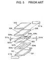
- a conventional radio frequency filter generally has a structure as shown in Fig. 5.
- the structure is as follows:
- resonator electrode 504a and capacitor electrode 507a, and resonator electrode 504b and capacitor electrode 507b are respectively disposed so as to be at least partly opposed to each other via dielectric layer 505.
- transmission electrode 506a, capacitor electrode 507a, transmission electrode 506b, capacitor electrode 507b and transmission electrode 506c are formed in order between terminal electrodes 511c and 511d, thereby forming a transmission line.
- terminal electrode 511a is connected to ground electrodes 502 and 509 for the purpose of grounding.
- terminal electrode 511b is connected to ground electrodes 502 and 509, and to each end of resonator electrodes 504a and 504b for the purpose of grounding.
- resonator electrodes 504a and 504b are of triplate structure sandwiched between two ground electrodes 502 and 509.
- Resonator electrodes 504a and 504b, one end of each electrode being grounded operate as a quarter-wavelength resonator, that is, as a serial resonator.
- these resonators are partly opposed to capacitors 507a and 507b respectively via dielectric layer 505, and operate as a parallel-plate capacitor. More specifically, two serial resonators with one end grounded are connected in shunt to the transmission line between terminal electrodes 511c and 511d via the parallel-plate capacitor. Accordingly, this filter operates as a band-stop filter having terminal electrodes 511c and 511d as input terminal and output terminal respectively.
- each electrode is formed by a plurality of electrode layers having predetermined dimensions inside dielectric layers.
- a filter having a predetermined frequency characteristic is selected by measurement.
- electrode layers are required to ensure higher dimensional accuracy. Thus it is difficult for such conventional forming process to ensure the required characteristics.
- the conventional method is unable to reduce the electrode dimensions while maintaining high accuracy and is limited with respect to reduction in size of the filter.
- the object of the present invention is to provide a small-sized radio frequency filter with which the desired frequency characteristic can be obtained with simple configuration even in higher frequency band.
- the radio frequency filter of the present invention includes an inductor component, capacitor component, and resistor component, and has a configuration as follows.
- a conductor pattern is formed on the surface of a dielectric layer, forming at least one of the inductor component, capacitance component and resistor component.
- An adjusting layer is formed so as to cover at least a part of the conductor pattern and serves to adjust the frequency characteristic of the filter.
- the conductor pattern is usually formed on the surface of dielectric layer, and sintered thereafter.
- the present invention has the following features.
- the present invention having a configuration as described above may provide a small-sized radio frequency filter by which the desired frequency characteristic can be easily obtained with simple configuration even in a higher frequency band.
- Fig. 1 is a configuration diagram of a radio frequency filter in the embodiment 1 of the present invention.
- Fig. 2 is a configuration diagram of a radio frequency filter in the embodiment 2 of the present invention.
- Fig. 3 is a configuration diagram of a radio frequency filter in the embodiment 3 of the present invention.
- Fig. 4 is a configuration diagram of a radio frequency filter in the embodiment 4 of the present invention.
- Fig. 5 is a configuration diagram of a radio frequency filter in a conventional example.
- Fig. 1 is a configuration diagram of a radio frequency filter in the embodiment 1 of the present invention.
- ground electrode 102 is formed on the under surface of dielectric 101, and terminal electrodes 103a, 103b, 103c, 103d, 103e, 103f are formed so as to go round the side of dielectric 101 and partly be routed to the top thereof.
- dielectric layer 109 is laminated on the upper side of these electrodes, on which adjusting dielectric layers 110a and 110b are respectively formed so as to be at least partly overlapped with first interdigital electrode 107a/107b and second interdigital electrode 108a/108b.
- first transmission electrode 104 and one end of second transmission electrode 105 are connected to terminal electrode 103a.
- first interdigital electrode 107a is connected to the other end of second transmission electrode 105
- terminal electrode 103d is connected to the other electrode of first inter digital electrode 107b.
- the other end of first transmission electrode 104 and one end of third transmission electrode 106 are connected to terminal electrode 103c.
- second interdigital electrode 108a is connected to the other end of third transmission electrode 106
- terminal electrode 103f is connected to third interdigital electrode 108b.
- terminal electrodes 103b, 103d, 103e and 103f are all connected to ground electrode 102 for the purpose of grounding.
- Interdigital electrodes 107a/ 107b are closely disposed without contacting each other. These operate as an interdigital capacitor whose capacity value is determined by the electrode dimension, the number of electrodes, the distance between electrodes, and the dielectric constant of dielectric 101. Interdigital electrodes 108a/108b works in the same way. Moreover, transmission electrode 105 operates as an inductor whose inductance is proportional to the characteristic impedance determined by the shape and dimension of the transmission line, and the dielectric constant of dielectric 101. Transmission electrode 106 works in the same constitution. More specifically, a serial resonator including transmission electrode 105 that operates as an inductor, and interdigital electrode 107a/107b that operates as a capacitor is connected in shunt to transmission line 104.
- Transmission electrode 106 and interdigital electrodes 108a/ 108b work in the same way.
- the serial resonator connected in shunt to the transmission line has an attenuation pole.
- the radio frequency filter of the present embodiment operates as a band-stop filter having two attenuation poles in which terminal electrode 103a and terminal electrode 103c respectively function as input terminal and output terminal.
- Dielectric layer 109 protects each electrode formed on the top surface of dielectric 101, thereby preventing them from being broken down or damaged. Adjusting dielectric layers 110a and 110b are formed so as to cover interdigital electrodes 107a/ 107b and 108a/ 108b respectively. Accordingly, the effective dielectric constant of the portion covered becomes greater as compared with the portion not covered, causing their capacity values to become greater. Moreover, dielectric whose sintering temperature is lower than the sintering temperature for dielectric 101 and dielectric layer 109 is used as the material for adjusting dielectric layers 110a and 110b. In this way, the adjusting dielectric layer can be formed in the final sintering process. Accordingly, it becomes possible to adjust the frequency characteristic after manufacturing the radio frequency filter. As an example, in the case of using thermosetting resin, it has been experimentally confirmed that the interdigital capacitor is increased by 20% in capacity.
- Fig. 2 is a configuration diagram of the radio frequency filter in the embodiment 2 of the present invention.
- the difference from the embodiment 1 of the radio frequency filter in the present embodiment is the forming position of the adjusting dielectric layer.
- adjusting dielectric layers 210a and 210b are formed so as to be overlapped with at least a part of transmission electrodes 105 and 106 on the top surface of dielectric layer 109 as shown in Fig. 2.
- the frequency characteristic of the radio frequency filter can be adjusted by changing the effective dielectric constant of these transmission electrodes, thereby adjusting the inductance value of the inductor.
- an adjusting magnetic layer can be formed instead of an adjusting dielectric layer. In this case, it is possible to increase the inductance value adjustable range.
- an adjusting conductor layer can be formed instead of an adjusting dielectric layer. Also in this case, it is possible to increase the capacity value or inductance value adjustable range.
- Fig. 3 is a configuration diagram of the radio frequency filter in the embodiment 3 of the present invention.
- adjusting conductor layers 310a and 310b are provided instead of the adjusting dielectric layers in the embodiment 1 which are grounded by using terminal electrodes 303d and 303f. Except the above, the configuration is in the same constitution as the embodiment 1.
- adjusting dielectric conductor layers 310a and 310b are formed on the interdigital electrodes, and the capacitances are added thereto in proportion to the area occupied by the interdigital electrode. Accordingly, it is possible to increase the capacitance value adjustable range.
- Fig. 4 is a configuration diagram of the radio frequency filter in the embodiment 4 of the present invention.
- adjusting conductor layers 410a and 410b are disposed so as to be at least partly overlapped with transmission electrodes 105 and 106 on the top surface of dielectric layer 109. Further, they are grounded by using grounding electrode 403e as shown in Fig. 4.
- the configuration other than the above is in the same constitution as that in the embodiment 2.
- transmission electrodes 105 and 106 are of triplate structure, and their electromagnetic field is concentrated between ground electrode 102 and conductor layers 410a and 410b. Accordingly, it is possible to increase the effective dielectric constant near transmission electrodes and to enlarge the inductance value adjustable range.
- each electrode can be formed so as for the line width and the line space to be not more than 60 ⁇ m. As a result, it is possible to make the radio frequency filter smaller and thinner as compared with a conventional radio frequency filter.
- the radio frequency filter in each of the embodiments operates as a band-stop filter. Further, with the addition of the conditions mentioned below, it is possible to allow the filter function as a filter other than a band-stop filter.
- the impedance is capacitive when the frequency is lower than the resonance frequency and is inductive when higher. Accordingly, when the frequency is between both resonance frequencies, the reactance components of the two resonators cancel each other. In that case, the shapes and dimensions of second transmission electrode 105 and first interdigital electrodes 107a/107b, and third transmission electrode 106 and second interdigital electrodes 108a/108b are set so that the reactance components become zero or nearly zero. As a result, the radio frequency filter operates as a band-pass filter having a pass-band within the band between the two resonance frequencies.
- the present invention having a configuration as described above provides a small-sized radio frequency filter by which the desired frequency characteristic can be obtained with a simple configuration even in higher frequency band.
Landscapes
- Control Of Motors That Do Not Use Commutators (AREA)
- Filters And Equalizers (AREA)
Abstract
Description
- The present invention mainly relates to a radio frequency filter used for mobile communication equipment such as a mobile phone.
- Recently, with the increase in needs for mobile communications equipment such as a mobile phone, the frequency band used for them has become insufficient in band width, giving rise to a trend of shifting to a higher frequency band. Accordingly, it is necessary for mobile communication equipment such as mobile phones to be compatible with a higher frequency. Above all, radio frequency filters used for them are becoming less in relative band width, and their component circuit elements are required to ensure higher dimensional accuracy.
- A conventional radio frequency filter generally has a structure as shown in Fig. 5. The structure is as follows:
- (1)
First ground electrode 502 is formed on the top surface of firstdielectric layer 501, and seconddielectric layer 503 is laminated onground electrode 502. - (2) Two
resonator electrodes dielectric layer 503, and thirddielectric layer 505 is laminated onresonators - (3)
First transmission electrode 506a,second transmission electrode 506b,third transmission electrode 506c,first capacitor electrode 507a andsecond capacitor electrode 507b are formed on the top surface ofdielectric layer 505, and fourthdielectric layer 508 is laminated on these electrodes. - (4)
Second ground electrode 509 is formed on the top surface ofdielectric layer 508, and fifthdielectric layer 510 is laminated onground electrode 509. - (5)
Terminal electrodes dielectric layer 510. -
- Here,
resonator electrode 504a andcapacitor electrode 507a, andresonator electrode 504b andcapacitor electrode 507b are respectively disposed so as to be at least partly opposed to each other viadielectric layer 505. As shown in Fig. 5,transmission electrode 506a,capacitor electrode 507a,transmission electrode 506b,capacitor electrode 507b andtransmission electrode 506c are formed in order betweenterminal electrodes terminal electrode 511a is connected toground electrodes terminal electrode 511b is connected toground electrodes resonator electrodes - In a conventional radio frequency filter having a structure as described above,
resonator electrodes ground electrodes Resonator electrodes capacitors dielectric layer 505, and operate as a parallel-plate capacitor. More specifically, two serial resonators with one end grounded are connected in shunt to the transmission line betweenterminal electrodes terminal electrodes - In a conventional radio frequency filter having the structure and operation as described above, each electrode is formed by a plurality of electrode layers having predetermined dimensions inside dielectric layers. After the electrode layer forming process followed by a dielectric layer sintering process, a filter having a predetermined frequency characteristic is selected by measurement. However, as recent equipment becomes higher in frequency, causing the relative bandwidth of frequency characteristic of the filter to become narrower, electrode layers are required to ensure higher dimensional accuracy. Thus it is difficult for such conventional forming process to ensure the required characteristics. Moreover, since electrode layers have been formed by using screen printing technique in most cases, there has been a problem of worsening of the dimensional accuracy such as "blurring of printing." Accordingly, the conventional method is unable to reduce the electrode dimensions while maintaining high accuracy and is limited with respect to reduction in size of the filter.
- The object of the present invention is to provide a small-sized radio frequency filter with which the desired frequency characteristic can be obtained with simple configuration even in higher frequency band.
- The radio frequency filter of the present invention includes an inductor component, capacitor component, and resistor component, and has a configuration as follows.
- A conductor pattern is formed on the surface of a dielectric layer, forming at least one of the inductor component, capacitance component and resistor component.
- An adjusting layer is formed so as to cover at least a part of the conductor pattern and serves to adjust the frequency characteristic of the filter.
- The conductor pattern is usually formed on the surface of dielectric layer, and sintered thereafter.
- The present invention has the following features.
- (1) Forming an adjusting layer with a dielectric material, it is possible to increase the frequency adjusting range by changing the effective dielectric constant.
- (2) Forming an adjusting layer with a magnetic material, it is possible to increase the frequency adjusting range by changing the effective permeability.
- (3) Forming a conductor on the top surface of adjusting layer formed of the dielectric material or magnetic material, it is possible to enhance the change of the effective dielectric constant or effective permeability.
- (4) Grounding the adjusting layer in (3), it is possible to further enhance the change of the effective dielectric constant or effective permeability.
- (5) Forming a dielectric layer between the conductor pattern and the adjusting layer, it is possible to prevent the breakdown or damage of electrodes not to be adjusted.
- (6) The adjustment can be regulated by changing the area of the adjusting layer for each conductor pattern of the adjusting object.
- (7) The frequency can be adjusted higher by removing a part of the adjusting layer.
- (8) The frequency can be adjusted lower by adding a part of the adjusting layer thereon.
- (9) The capacity value of the capacitor can be adjusted by forming at least a pair of interdigital electrodes in the conductor pattern.
- (10) The inductance value of the inductor can be adjusted by forming the conductor pattern, making at least one of the line width and the line space thereof not more than 60 µm.
- (11) Using intaglio-printing technique for forming the conductor pattern, it is possible to make the filter small-sized and adjustable.
- (12) Using thin-film forming technique for forming the conductor pattern, it is possible to make the filter small-sized and adjustable.
-
- The present invention having a configuration as described above may provide a small-sized radio frequency filter by which the desired frequency characteristic can be easily obtained with simple configuration even in a higher frequency band.
- Fig. 1 is a configuration diagram of a radio frequency filter in the embodiment 1 of the present invention.
- Fig. 2 is a configuration diagram of a radio frequency filter in the embodiment 2 of the present invention.
- Fig. 3 is a configuration diagram of a radio frequency filter in the embodiment 3 of the present invention.
- Fig. 4 is a configuration diagram of a radio frequency filter in the embodiment 4 of the present invention.
- Fig. 5 is a configuration diagram of a radio frequency filter in a conventional example.
- The preferred embodiments of the present invention will be described in the following with reference to the drawings.
- Fig. 1 is a configuration diagram of a radio frequency filter in the embodiment 1 of the present invention. In the radio frequency filter of the present embodiment,
ground electrode 102 is formed on the under surface of dielectric 101, andterminal electrodes first transmission electrode 104,second transmission electrode 105,third transmission electrode 106, firstinterdigital electrode 107a/107b, and secondinterdigital electrode 108a/ 108b. Further,dielectric layer 109 is laminated on the upper side of these electrodes, on which adjustingdielectric layers interdigital electrode 107a/107b and secondinterdigital electrode 108a/108b. One end offirst transmission electrode 104 and one end ofsecond transmission electrode 105 are connected toterminal electrode 103a. Moreover, one end of firstinterdigital electrode 107a is connected to the other end ofsecond transmission electrode 105, andterminal electrode 103d is connected to the other electrode of first interdigital electrode 107b. Similarly, the other end offirst transmission electrode 104 and one end ofthird transmission electrode 106 are connected toterminal electrode 103c. In addition, secondinterdigital electrode 108a is connected to the other end ofthird transmission electrode 106, andterminal electrode 103f is connected to thirdinterdigital electrode 108b. Further,terminal electrodes ground electrode 102 for the purpose of grounding. - The operation of a radio frequency filter having a configuration as described above will be described in the following.
-
Interdigital electrodes 107a/ 107b are closely disposed without contacting each other. These operate as an interdigital capacitor whose capacity value is determined by the electrode dimension, the number of electrodes, the distance between electrodes, and the dielectric constant ofdielectric 101.Interdigital electrodes 108a/108b works in the same way. Moreover,transmission electrode 105 operates as an inductor whose inductance is proportional to the characteristic impedance determined by the shape and dimension of the transmission line, and the dielectric constant ofdielectric 101.Transmission electrode 106 works in the same constitution. More specifically, a serial resonator includingtransmission electrode 105 that operates as an inductor, andinterdigital electrode 107a/107b that operates as a capacitor is connected in shunt totransmission line 104.Transmission electrode 106 andinterdigital electrodes 108a/ 108b work in the same way. The serial resonator connected in shunt to the transmission line has an attenuation pole. Accordingly, the radio frequency filter of the present embodiment operates as a band-stop filter having two attenuation poles in whichterminal electrode 103a andterminal electrode 103c respectively function as input terminal and output terminal. -
Dielectric layer 109 protects each electrode formed on the top surface ofdielectric 101, thereby preventing them from being broken down or damaged. Adjustingdielectric layers interdigital electrodes 107a/ 107b and 108a/ 108b respectively. Accordingly, the effective dielectric constant of the portion covered becomes greater as compared with the portion not covered, causing their capacity values to become greater. Moreover, dielectric whose sintering temperature is lower than the sintering temperature fordielectric 101 anddielectric layer 109 is used as the material for adjustingdielectric layers - Fig. 2 is a configuration diagram of the radio frequency filter in the embodiment 2 of the present invention. The difference from the embodiment 1 of the radio frequency filter in the present embodiment is the forming position of the adjusting dielectric layer. In the present embodiment, adjusting
dielectric layers transmission electrodes dielectric layer 109 as shown in Fig. 2. In this case, the frequency characteristic of the radio frequency filter can be adjusted by changing the effective dielectric constant of these transmission electrodes, thereby adjusting the inductance value of the inductor. - In the case of the radio frequency filter of the present embodiment, an adjusting magnetic layer can be formed instead of an adjusting dielectric layer. In this case, it is possible to increase the inductance value adjustable range. In the case of the radio frequency filter of the embodiments 1 and 2, an adjusting conductor layer can be formed instead of an adjusting dielectric layer. Also in this case, it is possible to increase the capacity value or inductance value adjustable range.
- Fig. 3 is a configuration diagram of the radio frequency filter in the embodiment 3 of the present invention. In the radio frequency filter of the present embodiment, as shown in Fig. 3, adjusting
conductor layers terminal electrodes dielectric conductor layers - Fig. 4 is a configuration diagram of the radio frequency filter in the embodiment 4 of the present invention. In the radio frequency filter of the present embodiment, as shown in Fig. 4, instead of adjusting dielectric layers in the embodiment 2, adjusting
conductor layers transmission electrodes dielectric layer 109. Further, they are grounded by usinggrounding electrode 403e as shown in Fig. 4. The configuration other than the above is in the same constitution as that in the embodiment 2. In this case,transmission electrodes ground electrode 102 andconductor layers - In each of the embodiments described above, it is also preferable to adjust the frequency by increasing or decreasing the area of the dielectric layer formed on the top surface of each electrode in order to protect the electrode. In this case, it is advantageous in that the radio frequency filter manufacturing processes may be reduced.
- In addition, since the above radio frequency filter includes transmission electrodes and interdigital electrodes, it is possible to make the electrode layer in single layer and to manufacture the radio frequency filters by using intaglio-printing technique or thin-film forming technique. Accordingly, in the radio frequency filter of the present invention, each electrode can be formed so as for the line width and the line space to be not more than 60 µm. As a result, it is possible to make the radio frequency filter smaller and thinner as compared with a conventional radio frequency filter.
- Further, in the serial resonator in each of the above embodiments, one end is connected to the transmission line between the input and output terminals, and the other end is grounded. Accordingly, the radio frequency filter in each of the embodiments operates as a band-stop filter. Further, with the addition of the conditions mentioned below, it is possible to allow the filter function as a filter other than a band-stop filter.
- Since each of the two serial resonators has an attenuation pole, the impedance is capacitive when the frequency is lower than the resonance frequency and is inductive when higher. Accordingly, when the frequency is between both resonance frequencies, the reactance components of the two resonators cancel each other. In that case, the shapes and dimensions of
second transmission electrode 105 and firstinterdigital electrodes 107a/107b, andthird transmission electrode 106 and secondinterdigital electrodes 108a/108b are set so that the reactance components become zero or nearly zero. As a result, the radio frequency filter operates as a band-pass filter having a pass-band within the band between the two resonance frequencies. - In such a band-pass filter, it is possible to adjust the frequency characteristic of the filter after manufacturing the filter. Furthermore, in the manufacturing process of mobile communication equipment such as mobile phones, it is possible to adjust the frequency characteristic of the filter after assembling the circuit components. As a result, the yield can be improved with respect to the manufacture of the equipment.
- The present invention having a configuration as described above provides a small-sized radio frequency filter by which the desired frequency characteristic can be obtained with a simple configuration even in higher frequency band.
Claims (13)
- A radio frequency filter, comprising:a dielectric layer;a conductor pattern formed on a surface of said dielectric layer, having at least one of an inductor component, a capacitance component, and a resistance component; andan adjusting layer, formed so as to cover at least a part of said conductor pattern, for adjusting a frequency characteristic of said radio frequency filter.
- The radio frequency filter of claim 1,
wherein said adjusting layer is formed of a dielectric material. - The radio frequency filter of claim 1,
wherein said adjusting layer is formed of a magnetic material. - The radio frequency filter of claim 1,
wherein said adjusting layer is formed of one of a dielectric material and a magnetic material, and a conductor for adjusting the frequency characteristic of said radio frequency filter is formed on a top surface of said adjusting layer. - The radio frequency filter of claim 4,
wherein said conductor is grounded. - The radio frequency filter of claim 1,
wherein a dielectric layer for protecting said conductor pattern is formed between said conductor patter and said adjusting layer. - The radio frequency filter of claim 1,
wherein an area of said adjusting layer is adjusted for each of said conductor patterns. - The radio frequency filter of claim 1,
wherein the frequency characteristic is adjusted by removing at least a part of said adjusting layer therefrom. - The radio frequency filter of claim 1,
wherein the frequency characteristic is adjusted by adding a part of said adjusting layer thereon. - The radio frequency filter of claim 1,
wherein said conductor pattern has at least a pair of interdigital electrodes. - The radio frequency filter of claim 1,
wherein at least one of a line width and a line space of said conductor pattern is not more than 60 µm. - The radio frequency filter of claim 1,
wherein said conductor pattern is formed by an intaglio-printing technique. - The radio frequency filter of claim 1,
wherein said conductor pattern is formed by an thin-film forming technique.
Applications Claiming Priority (2)
| Application Number | Priority Date | Filing Date | Title |
|---|---|---|---|
| JP2001049916A JP2002252534A (en) | 2001-02-26 | 2001-02-26 | High frequency filter |
| JP2001049916 | 2001-02-26 |
Publications (2)
| Publication Number | Publication Date |
|---|---|
| EP1239532A1 true EP1239532A1 (en) | 2002-09-11 |
| EP1239532B1 EP1239532B1 (en) | 2004-04-21 |
Family
ID=18910951
Family Applications (1)
| Application Number | Title | Priority Date | Filing Date |
|---|---|---|---|
| EP02004140A Expired - Lifetime EP1239532B1 (en) | 2001-02-26 | 2002-02-25 | Radio frequency filter |
Country Status (5)
| Country | Link |
|---|---|
| US (1) | US6577208B2 (en) |
| EP (1) | EP1239532B1 (en) |
| JP (1) | JP2002252534A (en) |
| CN (1) | CN1280986C (en) |
| DE (1) | DE60200387T2 (en) |
Families Citing this family (20)
| Publication number | Priority date | Publication date | Assignee | Title |
|---|---|---|---|---|
| US7091800B2 (en) * | 2001-06-21 | 2006-08-15 | Murata Manufacturing Co., Ltd. | Noise filter |
| US6898846B2 (en) * | 2002-08-21 | 2005-05-31 | Potomac Photonics, Inc. | Method and components for manufacturing multi-layer modular electrical circuits |
| JP3937433B2 (en) * | 2002-09-17 | 2007-06-27 | 日本電気株式会社 | Planar circuit-waveguide connection structure |
| JP3859573B2 (en) * | 2002-10-21 | 2006-12-20 | 富士通メディアデバイス株式会社 | Surface acoustic wave filter and filter device |
| US7652636B2 (en) * | 2003-04-10 | 2010-01-26 | Avery Dennison Corporation | RFID devices having self-compensating antennas and conductive shields |
| US7501984B2 (en) * | 2003-11-04 | 2009-03-10 | Avery Dennison Corporation | RFID tag using a surface insensitive antenna structure |
| US7055754B2 (en) * | 2003-11-03 | 2006-06-06 | Avery Dennison Corporation | Self-compensating antennas for substrates having differing dielectric constant values |
| US6928726B2 (en) * | 2003-07-24 | 2005-08-16 | Motorola, Inc. | Circuit board with embedded components and method of manufacture |
| JP2005328025A (en) | 2004-04-13 | 2005-11-24 | Matsushita Electric Ind Co Ltd | Method for manufacturing surface-mounted electronic component, surface-mounted electronic component manufactured by this manufacturing method, and electronic device using the same |
| US7501955B2 (en) * | 2004-09-13 | 2009-03-10 | Avery Dennison Corporation | RFID device with content insensitivity and position insensitivity |
| US7286366B2 (en) * | 2005-03-24 | 2007-10-23 | Motorola, Inc. | Multilayer circuit board with embedded components and method of manufacture |
| US7872844B2 (en) * | 2005-09-07 | 2011-01-18 | Panasonic Corporation | Composite electronic device |
| US7667557B2 (en) * | 2005-12-06 | 2010-02-23 | Tdk Corporation | Thin-film bandpass filter using inductor-capacitor resonators |
| TWI268745B (en) * | 2005-12-08 | 2006-12-11 | Ind Tech Res Inst | A multilayer printed circuit board embedded with a filter |
| US8067253B2 (en) | 2005-12-21 | 2011-11-29 | Avery Dennison Corporation | Electrical device and method of manufacturing electrical devices using film embossing techniques to embed integrated circuits into film |
| CN101589505A (en) * | 2007-02-01 | 2009-11-25 | 株式会社村田制作所 | Resonant element and manufacture method thereof |
| JP2010062260A (en) * | 2008-09-02 | 2010-03-18 | Fdk Corp | Laminated chip component and its manufacturing method |
| JP2010147746A (en) * | 2008-12-18 | 2010-07-01 | Mitsumi Electric Co Ltd | Antenna device |
| CN115428255B (en) * | 2020-08-25 | 2025-07-11 | 株式会社藤仓 | Filter device |
| US12394875B2 (en) | 2020-08-25 | 2025-08-19 | Fujikura Ltd. | Filter device comprising a substrate having strip-shaped conductors and ground recesses of lengths longer than the strip-shaped conductors |
Citations (3)
| Publication number | Priority date | Publication date | Assignee | Title |
|---|---|---|---|---|
| US5400000A (en) * | 1991-02-15 | 1995-03-21 | Murata Manufacturing Co., Ltd. | Band-pass filter having two loop-shaped electrodes |
| US5952901A (en) * | 1996-11-20 | 1999-09-14 | Alps Electric Co., Ltd. | Laminated electronic component with trimmable parallel electrodes |
| US5965494A (en) * | 1995-05-25 | 1999-10-12 | Kabushiki Kaisha Toshiba | Tunable resonance device controlled by separate permittivity adjusting electrodes |
Family Cites Families (10)
| Publication number | Priority date | Publication date | Assignee | Title |
|---|---|---|---|---|
| US4157517A (en) * | 1977-12-19 | 1979-06-05 | Motorola, Inc. | Adjustable transmission line filter and method of constructing same |
| US4706050A (en) * | 1984-09-22 | 1987-11-10 | Smiths Industries Public Limited Company | Microstrip devices |
| US5101182A (en) * | 1991-01-04 | 1992-03-31 | The United States Of America As Represented By The Secretary Of The Army | Drop-in magnetically tunable microstrip bandpass filter |
| JP3642110B2 (en) * | 1996-06-11 | 2005-04-27 | 松下電器産業株式会社 | Manufacturing method of electronic parts |
| JPH1032429A (en) * | 1996-07-18 | 1998-02-03 | Matsushita Electric Ind Co Ltd | Voltage controlled resonator and adjustment method thereof |
| JP3481069B2 (en) * | 1997-02-26 | 2003-12-22 | 日本特殊陶業株式会社 | Multilayer circuit with trimming capacitor |
| US6075713A (en) * | 1997-04-15 | 2000-06-13 | Motorola, Inc. | Laser trimmable electronic device |
| US5929729A (en) * | 1997-10-24 | 1999-07-27 | Com Dev Limited | Printed lumped element stripline circuit ground-signal-ground structure |
| US6175727B1 (en) * | 1998-01-09 | 2001-01-16 | Texas Instruments Israel Ltd. | Suspended printed inductor and LC-type filter constructed therefrom |
| JP2000323901A (en) * | 1999-05-07 | 2000-11-24 | Murata Mfg Co Ltd | Stacked lc filter |
-
2001
- 2001-02-26 JP JP2001049916A patent/JP2002252534A/en active Pending
-
2002
- 2002-02-25 EP EP02004140A patent/EP1239532B1/en not_active Expired - Lifetime
- 2002-02-25 DE DE60200387T patent/DE60200387T2/en not_active Expired - Fee Related
- 2002-02-26 CN CN02106511.XA patent/CN1280986C/en not_active Expired - Fee Related
- 2002-02-26 US US10/085,998 patent/US6577208B2/en not_active Expired - Fee Related
Patent Citations (3)
| Publication number | Priority date | Publication date | Assignee | Title |
|---|---|---|---|---|
| US5400000A (en) * | 1991-02-15 | 1995-03-21 | Murata Manufacturing Co., Ltd. | Band-pass filter having two loop-shaped electrodes |
| US5965494A (en) * | 1995-05-25 | 1999-10-12 | Kabushiki Kaisha Toshiba | Tunable resonance device controlled by separate permittivity adjusting electrodes |
| US5952901A (en) * | 1996-11-20 | 1999-09-14 | Alps Electric Co., Ltd. | Laminated electronic component with trimmable parallel electrodes |
Non-Patent Citations (2)
| Title |
|---|
| GEVORGIAN S S ET AL: "CAD MODELS FOR MULTILAYERED SUBSTRATE INTERDIGITAL CAPACITORS", IEEE TRANSACTIONS ON MICROWAVE THEORY AND TECHNIQUES, IEEE INC. NEW YORK, US, vol. 44, no. 6, 1 June 1996 (1996-06-01), pages 896 - 904, XP000588980, ISSN: 0018-9480 * |
| ROSHEN W A: "Effect of finite thickness of magnetic substrate on planar inductors", IEEE TRANSACTIONS ON MAGNETICS, JAN. 1990, USA, vol. 26, no. 1, pages 270 - 275, XP002200327, ISSN: 0018-9464 * |
Also Published As
| Publication number | Publication date |
|---|---|
| CN1372379A (en) | 2002-10-02 |
| JP2002252534A (en) | 2002-09-06 |
| DE60200387T2 (en) | 2004-08-26 |
| DE60200387D1 (en) | 2004-05-27 |
| EP1239532B1 (en) | 2004-04-21 |
| US6577208B2 (en) | 2003-06-10 |
| US20020145487A1 (en) | 2002-10-10 |
| CN1280986C (en) | 2006-10-18 |
Similar Documents
| Publication | Publication Date | Title |
|---|---|---|
| EP1239532B1 (en) | Radio frequency filter | |
| US6542052B2 (en) | Monolithic LC components | |
| US7312676B2 (en) | Multilayer band pass filter | |
| US6448873B1 (en) | LC filter with suspended printed inductor and compensating interdigital capacitor | |
| US7432786B2 (en) | High frequency filter | |
| US5880649A (en) | Multilayered frequency separator | |
| KR0148749B1 (en) | Filter and its manufacturing method | |
| US7113588B2 (en) | Input-output balanced filter | |
| US6356244B1 (en) | Antenna device | |
| US8018305B2 (en) | Electronic component | |
| US20030129957A1 (en) | Multilayer LC filter | |
| US8400236B2 (en) | Electronic component | |
| JP4693587B2 (en) | Bandpass filter | |
| US5825264A (en) | Stripline laminate dielectric filter with input/output patterns overlapping resonator conductors | |
| JP2737063B2 (en) | Stripline filter | |
| JP2003069362A (en) | Diplexer | |
| JP4691853B2 (en) | Laminated LC composite parts | |
| JP2737062B2 (en) | Stripline filter | |
| JPH0514007A (en) | Stripline filter | |
| JP4130442B2 (en) | Front-end module for mobile communication equipment | |
| JP4185805B2 (en) | Multilayer dielectric filter | |
| KR100332879B1 (en) | Dielectric duplexer and method for manufacturing thereof | |
| JP2002075742A (en) | Balun transformer and its characteristic adjustment method | |
| JP4111344B2 (en) | Front-end module for mobile communication equipment | |
| JPH09260904A (en) | Dielectric filter and adjustment method thereof |
Legal Events
| Date | Code | Title | Description |
|---|---|---|---|
| PUAI | Public reference made under article 153(3) epc to a published international application that has entered the european phase |
Free format text: ORIGINAL CODE: 0009012 |
|
| AK | Designated contracting states |
Kind code of ref document: A1 Designated state(s): AT BE CH CY DE DK ES FI FR GB GR IE IT LI LU MC NL PT SE TR |
|
| AX | Request for extension of the european patent |
Free format text: AL;LT;LV;MK;RO;SI |
|
| 17P | Request for examination filed |
Effective date: 20020903 |
|
| 17Q | First examination report despatched |
Effective date: 20030210 |
|
| AKX | Designation fees paid |
Designated state(s): DE FR GB |
|
| GRAP | Despatch of communication of intention to grant a patent |
Free format text: ORIGINAL CODE: EPIDOSNIGR1 |
|
| GRAS | Grant fee paid |
Free format text: ORIGINAL CODE: EPIDOSNIGR3 |
|
| GRAA | (expected) grant |
Free format text: ORIGINAL CODE: 0009210 |
|
| AK | Designated contracting states |
Kind code of ref document: B1 Designated state(s): DE FR GB |
|
| REG | Reference to a national code |
Ref country code: GB Ref legal event code: FG4D |
|
| REG | Reference to a national code |
Ref country code: IE Ref legal event code: FG4D |
|
| REF | Corresponds to: |
Ref document number: 60200387 Country of ref document: DE Date of ref document: 20040527 Kind code of ref document: P |
|
| ET | Fr: translation filed | ||
| PLBE | No opposition filed within time limit |
Free format text: ORIGINAL CODE: 0009261 |
|
| STAA | Information on the status of an ep patent application or granted ep patent |
Free format text: STATUS: NO OPPOSITION FILED WITHIN TIME LIMIT |
|
| 26N | No opposition filed |
Effective date: 20050124 |
|
| PGFP | Annual fee paid to national office [announced via postgrant information from national office to epo] |
Ref country code: GB Payment date: 20070221 Year of fee payment: 6 |
|
| PGFP | Annual fee paid to national office [announced via postgrant information from national office to epo] |
Ref country code: DE Payment date: 20070222 Year of fee payment: 6 |
|
| PGFP | Annual fee paid to national office [announced via postgrant information from national office to epo] |
Ref country code: FR Payment date: 20070208 Year of fee payment: 6 |
|
| GBPC | Gb: european patent ceased through non-payment of renewal fee |
Effective date: 20080225 |
|
| REG | Reference to a national code |
Ref country code: FR Ref legal event code: ST Effective date: 20081031 |
|
| PG25 | Lapsed in a contracting state [announced via postgrant information from national office to epo] |
Ref country code: DE Free format text: LAPSE BECAUSE OF NON-PAYMENT OF DUE FEES Effective date: 20080902 |
|
| PG25 | Lapsed in a contracting state [announced via postgrant information from national office to epo] |
Ref country code: FR Free format text: LAPSE BECAUSE OF NON-PAYMENT OF DUE FEES Effective date: 20080229 |
|
| PG25 | Lapsed in a contracting state [announced via postgrant information from national office to epo] |
Ref country code: GB Free format text: LAPSE BECAUSE OF NON-PAYMENT OF DUE FEES Effective date: 20080225 |