EP1239522A2 - Semiconductor device having insulated gate bipolar transistor with dielectric isolation structure and method of manufacturing the same - Google Patents
Semiconductor device having insulated gate bipolar transistor with dielectric isolation structure and method of manufacturing the same Download PDFInfo
- Publication number
- EP1239522A2 EP1239522A2 EP02005216A EP02005216A EP1239522A2 EP 1239522 A2 EP1239522 A2 EP 1239522A2 EP 02005216 A EP02005216 A EP 02005216A EP 02005216 A EP02005216 A EP 02005216A EP 1239522 A2 EP1239522 A2 EP 1239522A2
- Authority
- EP
- European Patent Office
- Prior art keywords
- semiconductor region
- semiconductor
- type
- region
- gate electrode
- Prior art date
- Legal status (The legal status is an assumption and is not a legal conclusion. Google has not performed a legal analysis and makes no representation as to the accuracy of the status listed.)
- Withdrawn
Links
Images



Classifications
-
- H—ELECTRICITY
- H10—SEMICONDUCTOR DEVICES; ELECTRIC SOLID-STATE DEVICES NOT OTHERWISE PROVIDED FOR
- H10D—INORGANIC ELECTRIC SEMICONDUCTOR DEVICES
- H10D84/00—Integrated devices formed in or on semiconductor substrates that comprise only semiconducting layers, e.g. on Si wafers or on GaAs-on-Si wafers
-
- H—ELECTRICITY
- H10—SEMICONDUCTOR DEVICES; ELECTRIC SOLID-STATE DEVICES NOT OTHERWISE PROVIDED FOR
- H10D—INORGANIC ELECTRIC SEMICONDUCTOR DEVICES
- H10D12/00—Bipolar devices controlled by the field effect, e.g. insulated-gate bipolar transistors [IGBT]
- H10D12/01—Manufacture or treatment
-
- H—ELECTRICITY
- H10—SEMICONDUCTOR DEVICES; ELECTRIC SOLID-STATE DEVICES NOT OTHERWISE PROVIDED FOR
- H10D—INORGANIC ELECTRIC SEMICONDUCTOR DEVICES
- H10D12/00—Bipolar devices controlled by the field effect, e.g. insulated-gate bipolar transistors [IGBT]
- H10D12/01—Manufacture or treatment
- H10D12/031—Manufacture or treatment of IGBTs
-
- H—ELECTRICITY
- H10—SEMICONDUCTOR DEVICES; ELECTRIC SOLID-STATE DEVICES NOT OTHERWISE PROVIDED FOR
- H10D—INORGANIC ELECTRIC SEMICONDUCTOR DEVICES
- H10D12/00—Bipolar devices controlled by the field effect, e.g. insulated-gate bipolar transistors [IGBT]
- H10D12/411—Insulated-gate bipolar transistors [IGBT]
- H10D12/421—Insulated-gate bipolar transistors [IGBT] on insulating layers or insulating substrates, e.g. thin-film IGBTs
Definitions
- the present invention relates to a semiconductor device having an insulated gate bipolar transistor with a dielectric isolation structure and a method of manufacturing the same and, more particularly, to a semiconductor device used as a power IC, e.g., an IPD (Intelligent Power Device).
- a semiconductor device used as a power IC e.g., an IPD (Intelligent Power Device).
- IGBTs insulated gate bipolar transistors
- FIG. 1 is a cross-sectional view showing the structure of a lateral IGBT in a conventional dielectric isolated substrate.
- the above dielectric isolation structure isolates elements by a dielectric substance.
- an SOI (silicon on insulator) structure to be described below will be taken as an example.
- a silicon oxide film 102 is formed on an n - -type silicon layer 101.
- An n - -type silicon layer 103 is formed on this silicon oxide film 102.
- An SOI structure is formed by these n - -type silicon layer 101, silicon oxide film 102, and n - -type silicon layer 103.
- a gate electrode 105 is formed with a gate insulating film 104 interposed between the n - -type silicon layer 103 and the gate electrode 105.
- an emitter electrode 106 and a collector electrode 107 are formed apart from the gate electrode 105.
- a field oxide film 108 is formed on the n - -type silicon layer 103 between the gate electrode 105 and the collector electrode 107.
- the gate electrode 105 is made of a polysilicon film about 4,000 ⁇ thick.
- a p-type base diffusion layer 109 is formed in the n - -type silicon layer 103 from a portion below the gate electrode 105 to a portion below the emitter electrode 106.
- a p + -type diffusion layer 110 is formed between this p-type base diffusion layer 109 and the emitter electrode 106.
- an n + -type diffusion layer 111 is formed on the p-type base diffusion layer 109.
- An n-type buffer diffusion layer 112 is formed in the n - -type silicon layer 103 below the collector electrode 107.
- the main purpose of the n-type buffer diffusion layer 112 is to increase the collector-emitter withstand voltage.
- a p + -type diffusion layer 113 is formed between this n-type buffer diffusion layer 112 and the collector electrode 107.
- a lateral IGBT in the conventional dielectric isolation substrate is constructed as above.
- a parasitic npn transistor composed of the n + -type diffusion layer 111, the p-type base diffusion layer 109, and the n - -type silicon layer 103 easily operates and sometimes destroys the IGBT by latch up. That is, when this parasitic npn transistor operates, the base current of a parasitic pnp transistor made up of the p + -type diffusion layer 113, the n-type buffer diffusion layer 112, the n - -type silicon layer 103, and the p-type base diffusion layer 109 increases. This amplifies the collector-emitter current of this parasitic pnp transistor.
- the collector-emitter current increases and destroys the IGBT.
- the impurity concentration in the p-type base diffusion layer 109 is low, the latch-up phenomenon causes more easily. To prevent this, the impurity concentration in the p-type base diffusion layer 109 can be increased. However, this makes it difficult to form an inversion layer in the channel region below the gate electrode 105.
- a p-type diffusion layer 114 is formed below a p-type base diffusion layer 109 on the side of an emitter electrode 106.
- This p-type diffusion layer 114 is formed by ion implantation before the formation of a gate electrode 105.
- the present invention has been made in consideration of the above situation, and has as its object to provide a semiconductor device having a lateral IGBT capable of improving ruggedness by the latch-up phenomenon and reducing variations in the current-voltage characteristics, and to provide a method of manufacturing the same.
- a semiconductor device comprises: a first-conductivity-type semiconductor substrate having a principal surface; a second-conductivity-type first semiconductor region and a second-conductivity-type second semiconductor region formed apart from each other in the principal surface of the semiconductor substrate; a second-conductivity-type third semiconductor region formed on the first semiconductor region, the third semiconductor region having an impurity concentration higher than that of the first semiconductor region; a first-conductivity-type fourth semiconductor region formed on the third semiconductor region; a first main electrode formed on the fourth semiconductor region; a second main electrode formed on the second semiconductor region; and a gate electrode formed, at least on the first semiconductor region and on the principal surface of the semiconductor substrate between the fourth semiconductor region and the second semiconductor region, with a gate insulating film interposed between the gate electrode and the first semiconductor region and the principal surface of the semiconductor substrate.
- a manufacturing method of a semiconductor device comprises: forming a second-conductivity-type first semiconductor region in the surface of a first-conductivity-type semiconductor substrate; forming a gate insulating film on the first semiconductor region and on the semiconductor substrate; forming a gate electrode on the gate insulating film; forming a second semiconductor region having an impurity concentration higher than that of the first semiconductor region in the first semiconductor region, by ion implantation using self-alignment which uses the gate electrode as a mask material; forming a first-conductivity-type third semiconductor region on the second semiconductor region, by ion implantation using self-alignment which uses the gate electrode as a mask material; and forming a second-conductivity-type fourth semiconductor region apart from the first semiconductor region, on the surface of the semiconductor substrate.
- the impurity concentration in the third semiconductor region below the fourth semiconductor region is made higher than the impurity concentration in the first semiconductor region. That is, the resistivity of this third semiconductor region below the fourth semiconductor region is made lower than that of the first semiconductor region.
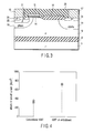
- FIG. 3 is a cross-sectional view showing the structure of a lateral IGBT in a dielectric isolated substrate according to the first embodiment of the present invention.
- a silicon oxide film (SiO 2 ) 12 as a dielectric isolation film is formed on an n - -type silicon semiconductor layer 11.
- An n - -type silicon semiconductor layer 13 is formed on this silicon oxide film 12.
- An SOI (Silicon On Insulator) substrate is formed by these n - -type silicon layer 11, silicon oxide film 12, and n - -type silicon layer 13.
- a gate electrode 15 is formed with a gate insulating film 14 interposed between the n - -type silicon layer 13 and the gate electrode 15.
- This gate insulating film 14 is a silicon oxide film.
- the gate electrode 15 is made of a polysilicon film and has a film thickness of about 5,000 ⁇ or more.
- an emitter electrode 16 and a collector electrode 17 are formed apart from the gate electrode 15.
- a field oxide film (SiO 2 ) 18 is formed on the n - -type silicon layer 13 between the gate electrode 15 and the collector electrode 17.
- a p-type base diffusion layer 19 is formed in the n - -type silicon layer 13 from a portion below the gate electrode 15 to a portion below the emitter electrode 16. Between this p-type base diffusion layer 19 and the emitter electrode 16, a p + -type diffusion layer 20 is so formed as to contact the emitter electrode 16. In addition, between the p-type base diffusion layer 19 and the emitter electrode 16, an n + -type diffusion layer 21 is so formed as to contact the emitter electrode 16. This n + -type diffusion layer 21 is formed from a portion below the emitter electrode 16 to a portion below the gate electrode 15 and functions as a current path of this IGBT.
- a p-type diffusion layer 22 is formed between the p-type base diffusion layer 19 and the p + - and n + -type diffusion layers 20 and 21.
- the p + -type diffusion layer 20 is in contact with the p-type diffusion layer 22, and the p-type diffusion layer 22 is in contact with the p-type base diffusion layer 19.
- the p + -type diffusion layer 20 is a contact layer having a function of stabilizing the potentials of the p-type diffusion layer 22 and the p-type base layer 19 at the same potential as the emitter electrode 16.
- This p-type diffusion layer 22 is formed by self-aligned ion implantation using the gate electrode 15 as a mask.
- boron (B) for example, is doped at an acceleration voltage of 100 keV or more and a dose of about 1.0 ⁇ 10 13 to about 1.0 ⁇ 10 14 cm -2 .
- boron (B) for example, is doped at an acceleration voltage of 30 to 100 keV or more and a dose of about 1.0 ⁇ 10 13 to about 1.0 ⁇ 10 15 cm -2 .
- This p-type base diffusion layer 19 is formed by performing annealing a plurality of times after the ion implantation.
- the p-type diffusion layer 22 is formed by performing annealing a smaller number of times than that for the p-type base diffusion layer 19, after the ion implantation is performed. Therefore, as shown in FIG. 3, the p-type base diffusion layer 19 is larger than the p-type diffusion layer 22 and has an impurity concentration lower than that of the p-type diffusion layer 22.
- n-type buffer diffusion layer 23 is formed in the n - -type silicon layer 13 below the collector electrode 17.
- a p + -type diffusion layer 24 is formed between this n-type buffer diffusion layer 23 and the collector electrode 17.
- a dielectric interlayer 25 is formed on the n - -type silicon layer 13 including the gate electrode 15 and the field oxide film 18.
- the lateral IGBT of the first embodiment is constructed as above.
- the p-type diffusion layer 22 covers the lower portions of the n + -type diffusion layer 21 and the p + -type diffusion layer 20 without diffusing to a channel region below the gate electrode 15.
- This channel region means a surface region of the p-type base diffusion layer 19 in contact with the gate insulating film 14 below the gate electrode 15.
- This can decrease the resistivity (increase the impurity concentration) in the region (p-type diffusion layer 22) below the n + -type diffusion layer 21.
- This makes the parasitic npn transistor described above difficult to operate, and also makes a parasitic pnp transistor difficult to operate.
- latch up occurring when these parasitic npn and pnp transistors operate can be prevented. Consequently, a large ON current flowing upon latch up can also be suppressed, so it is possible to protect this IGBT from being destroyed by such a large electric current. Accordingly, we can improve a capability of ruggedness by the latch-up phenomenon.
- FIG. 4 shows the maximum turn-off current of a conventional IGBT having no p-type diffusion layer 22 and that of the IGBT of this embodiment.
- the turn-off current is one index which indicates the current ruggedness of an IGBT.
- the maximum turn-off current of the IGBT of this embodiment is twice that of the conventional IGBT or more. This indicates that the electric current performance of the IGBT of this embodiment is twice that of the conventional IGBT or more.
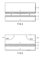
- FIGS. 5 to 10 are cross-sectional views showing the steps of the method of manufacturing the IGBT of the first embodiment.
- a silicon oxide film 12 is formed on an n - -type silicon semiconductor substrate 11.
- Another silicon oxide film 12 is formed on an n - -type silicon semiconductor substrate 13.
- the silicon oxide films 12 of the two silicon substrates 11 and 13 are adhered by bonding, thereby forming an SOI substrate as shown in FIG. 6.
- a p-type base diffusion layer 19 and an n-type buffer diffusion layer 23 are formed apart from each other by ion implantation.
- boron (B) for example, is doped at an acceleration voltage of 30 to 100 keV or more and a dose of about 1.0 ⁇ 10 13 to about 1.0 ⁇ 10 14 cm -2 .
- Both the p-type base diffusion layer 19 and the n-type buffer diffusion layer 23 are annealed after the doping of impurity ions, thereby forming regions of predetermined sizes.
- the depth of the p-type base diffusion layer 19 from the surface of the n - -type silicon substrate 13 is 1.5 to 4.0 ⁇ m.
- a field oxide film (SiO 2 ) 18 is formed by LOCOS on the n - -type silicon substrate 13 between the p-type base diffusion layer 19 and the n-type buffer diffusion layer 23.
- This field oxide film 18 is spaced a predetermined distance from the p-type base diffusion layer 19, and partially overlaps the n-type buffer diffusion layer 23.
- a silicon oxide film (gate insulating film) 14 is formed by thermal oxidation on the p-type base diffusion layer 19 and the n - -type silicon substrate 13.
- conductive polysilicon is deposited on the gate insulating film 14 to form a conductive polysilicon film.
- This conductive polysilicon film is then patterned to form a gate electrode 15.
- the film thickness of this gate electrode 15 is 5,000 ⁇ or more.
- ion implantation is performed by self-alignment using the gate electrode 15 as a mask material in the upper layer of the p-type base diffusion layer 19, forming a p-type diffusion layer 22.
- boron (B) for example, is doped at an acceleration voltage of 100 keV or more and a dose of about 1.0 ⁇ 10 13 to 1.0 ⁇ 10 15 cm -2 .
- the impurity concentration in the p-type diffusion layer 22 is higher than that in the p-type base diffusion layer 19.
- a p + -type diffusion layer 20 is formed in the upper layer of the p-type diffusion layer 22 by ion implantation.
- This ion implantation for forming the p + -type diffusion layer 20 is executed after a region except for the p + -type diffusion layer 20 is protected with a mask material.
- an n + -type diffusion layer 21 is formed by covering the p + -type diffusion layer 20 with a mask material and performing ion implantation by self-alignment using the gate electrode 15 as another mask material.
- a p + -type diffusion layer 24 is formed on the n-type buffer diffusion layer 23 by the same formation step as for the p + -type diffusion layer 20.
- All of the p-type diffusion layer 22, the p + -type diffusion layers 20 and 24, and the n + -type diffusion layer 21 are annealed after the doping of impurity ions, thereby forming regions of predetermined sizes.
- the depth of the p-type diffusion layer 22 from the surface of the n - -type silicon substrate 13 is less than that of the p-type base diffusion layer 19 from the surface of the n - -type silicon substrate 13.
- the depth of the p-type diffusion layer 22 is 1.0 to 1.2 ⁇ m.
- the depth of the p + -type diffusion layer 20 from the surface of the n - -type silicon substrate 13 is less than 0.5 ⁇ m.
- a dielectric interlayer 25 is formed by CVD. Subsequently, contact holes are formed by etching system (for example RIE) in the dielectric interlayer 25 on the p + -type diffusion layer 20, the n + -type diffusion layer 21, and the p + -type diffusion layer 24. A metal such as aluminum (Al) is buried in these contact holes. Unnecessary Al is removed by etching system (for example RIE) to form an emitter electrode 16 and a collector electrode 17 as shown in FIG. 3. Through the above steps, the lateral IGBT in the dielectric isolation substrate of the first embodiment is completed.
- etching system for example RIE
- a p-type impurity is doped by self-alignment using the gate electrode 15 as a mask material after the formation of the gate electrode 15, thereby forming the p-type diffusion layer 22. That is, the gate electrode 15 serves as a film for stopping the implantation of the p-type impurity when this p-type impurity is ion-implanted, thereby preventing the implantation of the p-type impurity into the channel region.
- the impurity doping for forming the p-type diffusion layer 22 is performed after the formation of the gate electrode 15, i.e., after the thermal diffusion of the p-type base diffusion layer 19 and the n-type buffer diffusion layer 23.
- ion implantation must be performed using a high acceleration voltage of 100 keV or more.
- the lower portion of the n + -type diffusion layer 21 can be covered with the p-type diffusion layer 22 without diffusing this p-type diffusion layer 22 to the channel region below the gate electrode 15. Accordingly, it is possible to decrease the resistivity (increase the impurity concentration) in the region below the n + -type diffusion layer 21. This makes it possible to reduce the influence of latch up produced by the combined effect of the parasitic npn and pnp transistors described earlier, and to improve a capability of ruggedness by the latch up phenomenon.
- the p-type diffusion layer 22 is formed by self-alignment using the gate electrode 15 as a mask material. This can eliminate a positional deviation of the p-type diffusion layer 22 from the gate electrode 15. Consequently, current-voltage characteristics having little variations can be obtained in the IGBT.
- the film thickness of polysilicon for forming the gate electrode 15 is 5,000 ⁇ or more. Accordingly, when ion implantation for forming the p-type diffusion layer 22 is performed, no impurity ions punch through the gate electrode 15 to reach the p-type base diffusion layer 19.
- FIG. 11A is a graph showing an impurity diffusion profile when the film thickness of the gate electrode 15 is 5,000 ⁇ or more.
- FIG. 11B is a graph showing an impurity diffusion profile when the film thickness of the gate electrode 15 is less than 5,000 ⁇ .
- FIGS. 11A and 11B demonstrate that if the film thickness of the gate electrode 15 is less than 5,000 ⁇ , p-type impurity ions punch through the gate electrode 15 to reach the channel region (p-type diffusion layer 22) below the gate electrode 15.
- FIG. 12 is a graph showing the current-voltage characteristics of the IGBT of the first embodiment.
- FIG. 12 also shows the current-voltage characteristics of a conventional IGBT.
- FIG. 12 shows that when the film thickness of the gate electrode 15 is 5,000 ⁇ or more, a collector-emitter voltage Vce and a threshold voltage Vth are almost the same as those of the conventional IGBT. However, if the film thickness of the gate electrode 15 is less than 5,000 ⁇ , both the collector-emitter voltage Vce and the threshold voltage Vth are higher than those of the conventional IGBT.
- the foregoing reveal that when the film thickness of the gate electrode 15 is 5,000 ⁇ or more, no p-type impurity ions punch through the gate electrode 15; if the film thickness of the gate electrode 15 is less than 5,000 ⁇ , p-type impurity ions punch through the gate electrode 15 to reach the channel region below this gate electrode 15.
- a power IC to which the IGBT of the above first embodiment is applied will be described below as the second embodiment.
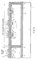
- FIG. 13 is a cross-sectional view showing the structure of this power IC having the IGBT structure, according to the second embodiment of the present invention.
- the IGBT of the first embodiment is formed in a region (power output portion) isolated by a polysilicon film 31 as a trench isolation film.
- the alternate long and short dashed lines in FIG. 13 correspond to a unit cell of the IGBT explained in the first embodiment.
- a diode is formed in another region (logic portion) isolated by the polysilicon film 31 as a trench isolation film.
- a field oxide film 18 is formed by the same step as the formation step of the field oxide film 18 of the IGBT. This field oxide film 18 is so formed that prospective anode and cathode regions of the Zener diode are open.
- a p-type diffusion layer 22 is formed by the same step as the formation step of the p-type diffusion layer 22 of the IGBT.
- a p + -type diffusion layer 20 is formed on this p-type diffusion layer 22 by the same step as the formation step of the p + -type diffusion layers 20 and 24 of the IGBT.
- an n + -type diffusion layer 21 is formed by the same step as the formation step of the n + -type diffusion layer 21 of the IGBT.
- a dielectric interlayer 25 is formed on the above structure by the same step as the formation step of the dielectric interlayer 25 of the IGBT.
- contact holes are formed by the same step as the formation step of the contact holes of the IGBT.
- a metal such as aluminum (Al) is buried in these contact holes by the same step as for the IGBT.
- unnecessary Al is removed by the same step (etching system (for example RIE) as for the IGBT, thereby forming an anode electrode 32 and a cathode electrode 33.
- the p-type diffusion layer 22 of the IGBT in the power output portion can be formed by using the formation step of the p-type diffusion layer 22 necessary in the logic portion. This fabrication method is advantageous because the number of manufacturing steps does not increase.
- each of the above embodiments includes inventions in various stages. So, these inventions in various stages can be extracted by properly combining a plurality of components disclosed in each embodiment.
- each embodiment of the present invention can provide a semiconductor device having a lateral IGBT capable of improving ruggedness by the latch-up phenomenon and reducing variations in the current-voltage characteristics, and to provide a method of manufacturing the same.
Landscapes
- Insulated Gate Type Field-Effect Transistor (AREA)
- Thin Film Transistor (AREA)
Abstract
Description
Claims (19)
- A semiconductor device characterized by comprising:a first-conductivity-type semiconductor substrate (13) having a principal surface;a second-conductivity-type first semiconductor region (19) and a second-conductivity-type second semiconductor region (24) formed apart from each other in the principal surface of said semiconductor substrate (13);a second-conductivity-type third semiconductor region (22) formed on said first semiconductor region (19), said third semiconductor region (22) having an impurity concentration higher than that of said first semiconductor region (19);a first-conductivity-type fourth semiconductor region (21) formed on said third semiconductor region (22);a first main electrode (16) formed on said fourth semiconductor region (21);a second main electrode (17) formed on said second semiconductor region (24); anda gate electrode (15) formed, at least on said first semiconductor region (19) and on the principal surface of said semiconductor substrate (13) between said fourth semiconductor region (21) and said second semiconductor region (24), with a gate insulating film (14) interposed between said gate electrode (15) and said first semiconductor region (19) and the principal surface of said semiconductor substrate (13).
- A semiconductor device according to claim 1, characterized by further comprising a fifth semiconductor region (20) formed between said third semiconductor region (22) and said first main electrode (16), said fifth semiconductor region (20) having an impurity concentration higher than that of said third semiconductor region (22).
- A semiconductor device according to claim 1, characterized in that said third semiconductor region (22) is formed by ion implantation using self-alignment which uses said gate electrode (15) as a mask material, and said third semiconductor region (22) does not reach a channel region formed on the surface of said first semiconductor region (19) below said gate electrode (15).
- A semiconductor device according to claim 1, characterized by further comprising a field insulating film (18) formed on said semiconductor substrate (13) between said gate electrode (15) and said second semiconductor region (24).
- A semiconductor device according to claim 1, characterized in that said semiconductor substrate (13) is an island region formed on a dielectric isolation layer (12).
- A semiconductor device according to claim 1, characterized in that said gate electrode (15) is made of a polysilicon film having a film thickness of not less than 5,000 Å.
- A semiconductor device according to claim 1, characterized in that said semiconductor device is an insulated gate bipolar transistor having said first semiconductor region (19) as a base, said third semiconductor region (21) as an emitter, and said second semiconductor region (24) as a collector.
- A manufacturing method of a semiconductor device characterized by comprising:forming a second-conductivity-type first semiconductor region (19) in the surface of a first-conductivity-type semiconductor substrate (13);forming a gate insulating film (14) on the first semiconductor region (19) and on the semiconductor substrate (13);forming a gate electrode (15) on the gate insulating film (14);forming a second semiconductor region (22) having an impurity concentration higher than that of the first semiconductor region (19) in the first semiconductor region (19), by ion implantation using self-alignment which uses the gate electrode (15) as a mask material;forming a first-conductivity-type third semiconductor region (21) on the second semiconductor region (22), by ion implantation using self-alignment which uses the gate electrode (15) as a mask material; andforming a second-conductivity-type fourth semiconductor region (24) apart from the first semiconductor region (19), on the surface of the semiconductor substrate (13).
- A manufacturing method of semiconductor device according to claim 8, characterized by further comprising forming a field insulating film (18) having a film thickness larger than that of the gate insulating film (14), on the semiconductor substrate (13) between the gate electrode (15) and the fourth semiconductor region (24).
- A manufacturing method of semiconductor device according to claim 8, characterized in that the semiconductor substrate (13) is an island region formed on a dielectric isolation layer (12).
- A manufacturing method of semiconductor device according to claim 8, characterized in that forming the second semiconductor region (22) comprises doping a p-type impurity at an acceleration voltage of not less than 100 keV and a dose of 1.0 × 10¹³ to 1.0 × 1015 cm-2.
- A manufacturing method of semiconductor device according to claim 11, characterized in that the gate electrode (15) is made of a polysilicon film having a film thickness of not less than 5,000 Å.
- A manufacturing method of semiconductor device according to claim 8, characterized in that the semiconductor device is an insulated gate bipolar transistor having the first semiconductor region (19) as a base, the third semiconductor region (21) as an emitter, and the second semiconductor region (24) as a collector.
- A manufacturing method of semiconductor device characterized by comprising:forming a first semiconductor region (19) by ion-implanting a second-conductivity-type impurity into a first-conductivity-type semiconductor substrate (13), and annealing the semiconductor substrate (13) to diffuse the impurity;forming a gate insulating film (14) on the first semiconductor region (19) and on the semiconductor substrate (13);forming a gate electrode (15) on the gate insulating film (14);performing first ion implantation for ion-implanting a second-conductivity-type impurity into the first semiconductor region (19), by using self-alignment which uses the gate electrode (15) as a mask material;performing second ion implantation for ion-implanting, into the first semiconductor region (19), a first-conductivity-type impurity to a position shallower than the first ion implantation, by using self-alignment which uses the gate electrode (15) as a mask material;performing third ion implantation for ion-implanting a second-conductivity-type impurity into that region of the semiconductor substrate (13), which is spaced apart from the first semiconductor region (19); andannealing the semiconductor substrate (13) to diffuse the impurities implanted by the first, second, and third ion implantations, after the first, second, and third ion implantations are completed, thereby forming a second semiconductor region (22), a third semiconductor region (21), and a fourth semiconductor region (24), the impurity concentration of the second semiconductor region (22) being higher than that of the first semiconductor region (19), the third semiconductor region (21) being positioned above the second semiconductor region (22), and the fourth semiconductor region (24) is being spaced apart from the first semiconductor region (19).
- A manufacturing method of semiconductor device according to claim 14, characterized by further comprising forming a field insulating film (18) having a film thickness larger than that of the gate insulating film (15), on the semiconductor substrate (13) between the gate electrode (15) and the fourth semiconductor region (24).
- A manufacturing method of semiconductor device according to claim 14, characterized in that the semiconductor substrate (13) is an island region formed on a dielectric isolation layer (12).
- A manufacturing method of semiconductor device according to claim 14, characterized in that forming the second semiconductor region (22) comprises doping a p-type impurity at an acceleration voltage of not less than 100 keV and a dose of 1.0 × 10¹³ to 1.0 × 1015 cm-2.
- A manufacturing method of semiconductor device according to claim 17, characterized in that the gate electrode (15) is made of a polysilicon film having a film thickness of not less than 5,000 Å.
- A manufacturing method of semiconductor device according to claim 14, characterized in that the semiconductor device is an insulated gate bipolar transistor having the first semiconductor region (19) as a base, the third semiconductor region (21) as an emitter, and the second semiconductor region (24) as a collector.
Applications Claiming Priority (2)
| Application Number | Priority Date | Filing Date | Title |
|---|---|---|---|
| JP2001063727 | 2001-03-07 | ||
| JP2001063727A JP2002270844A (en) | 2001-03-07 | 2001-03-07 | Semiconductor device and manufacturing method thereof |
Publications (2)
| Publication Number | Publication Date |
|---|---|
| EP1239522A2 true EP1239522A2 (en) | 2002-09-11 |
| EP1239522A3 EP1239522A3 (en) | 2004-05-19 |
Family
ID=18922666
Family Applications (1)
| Application Number | Title | Priority Date | Filing Date |
|---|---|---|---|
| EP02005216A Withdrawn EP1239522A3 (en) | 2001-03-07 | 2002-03-07 | Semiconductor device having insulated gate bipolar transistor with dielectric isolation structure and method of manufacturing the same |
Country Status (6)
| Country | Link |
|---|---|
| US (1) | US6677622B2 (en) |
| EP (1) | EP1239522A3 (en) |
| JP (1) | JP2002270844A (en) |
| KR (1) | KR100457413B1 (en) |
| CN (1) | CN1228857C (en) |
| TW (1) | TWI283067B (en) |
Cited By (3)
| Publication number | Priority date | Publication date | Assignee | Title |
|---|---|---|---|---|
| FR2863770A1 (en) * | 2003-12-12 | 2005-06-17 | Mitsubishi Electric Corp | SEMICONDUCTOR DEVICE OF THE DIELECTRIC SEPARATION TYPE AND METHOD OF MANUFACTURING THE SAME |
| DE102006043990B4 (en) * | 2006-01-31 | 2013-07-04 | Mitsubishi Electric Corp. | Semiconductor device |
| CN109494254A (en) * | 2018-10-16 | 2019-03-19 | 扬州国扬电子有限公司 | Improve the self-registered technology of grid-controlled type power device safety operation area performance |
Families Citing this family (30)
| Publication number | Priority date | Publication date | Assignee | Title |
|---|---|---|---|---|
| JP3701227B2 (en) * | 2001-10-30 | 2005-09-28 | 三菱電機株式会社 | Semiconductor device and manufacturing method thereof |
| JP2007194575A (en) | 2005-12-21 | 2007-08-02 | Mitsubishi Electric Corp | Semiconductor device |
| JP4952042B2 (en) * | 2006-04-27 | 2012-06-13 | 株式会社デンソー | Semiconductor device |
| JP5036234B2 (en) | 2006-07-07 | 2012-09-26 | 三菱電機株式会社 | Semiconductor device |
| JP2008147318A (en) * | 2006-12-08 | 2008-06-26 | Matsushita Electric Ind Co Ltd | High breakdown voltage semiconductor device and manufacturing method thereof |
| JP5261927B2 (en) | 2006-12-11 | 2013-08-14 | パナソニック株式会社 | Semiconductor device |
| KR100847306B1 (en) * | 2007-02-14 | 2008-07-21 | 삼성전자주식회사 | Semiconductor device and manufacturing method thereof |
| KR100906555B1 (en) | 2007-08-30 | 2009-07-07 | 주식회사 동부하이텍 | Insulated Gate Bipolar Transistor and Manufacturing Method Thereof |
| JP5272410B2 (en) | 2008-01-11 | 2013-08-28 | 富士電機株式会社 | Semiconductor device and manufacturing method thereof |
| JP2009194197A (en) * | 2008-02-15 | 2009-08-27 | Panasonic Corp | Semiconductor device and manufacturing method thereof |
| CN101431097B (en) * | 2008-12-11 | 2010-10-13 | 电子科技大学 | A thin-layer SOI LIGBT device |
| CN105097903B (en) * | 2009-11-09 | 2020-07-03 | 苏州博创集成电路设计有限公司 | Silicon-on-insulator lateral N-type insulated gate bipolar transistor |
| CN102983162A (en) * | 2011-09-05 | 2013-03-20 | 旺宏电子股份有限公司 | Semiconductor device and manufacturing method thereof |
| US10529866B2 (en) | 2012-05-30 | 2020-01-07 | X-Fab Semiconductor Foundries Gmbh | Semiconductor device |
| CN102769038B (en) * | 2012-06-30 | 2014-12-10 | 东南大学 | Latch-up resisting N-type SOI laterally diffused metal oxide semiconductor |
| CN102760761B (en) * | 2012-06-30 | 2014-12-03 | 东南大学 | Latch-preventing N type silicon on insulator transverse isolated gate bipolar transistor |
| CN102832232B (en) * | 2012-08-14 | 2014-12-10 | 东南大学 | Silicon-controlled rectifier lateral double diffused metal oxide semiconductor with high maintaining voltage |
| CN103219237B (en) * | 2013-04-27 | 2015-10-28 | 中国东方电气集团有限公司 | A kind of manufacture method of autoregistration insulated gate bipolar transistor |
| CN103219238B (en) * | 2013-04-27 | 2016-09-21 | 中国东方电气集团有限公司 | The igbt device of a kind of fully self aligned and manufacture method thereof |
| JP6479533B2 (en) * | 2015-03-31 | 2019-03-06 | ラピスセミコンダクタ株式会社 | Semiconductor device and manufacturing method of semiconductor device |
| CN105185826B (en) * | 2015-08-10 | 2019-01-22 | 电子科技大学 | A lateral RC-IGBT device |
| US9887288B2 (en) * | 2015-12-02 | 2018-02-06 | Texas Instruments Incorporated | LDMOS device with body diffusion self-aligned to gate |
| CN108321195B (en) * | 2018-02-05 | 2020-05-22 | 电子科技大学 | A short-circuit anode SOI LIGBT with anode pinch-off groove |
| CN109103240B (en) * | 2018-08-21 | 2021-08-20 | 电子科技大学 | A low on-power dissipation silicon-on-insulator lateral insulated gate bipolar transistor |
| CN109888006B (en) * | 2019-03-12 | 2021-08-20 | 电子科技大学 | A low-power silicon-on-insulator lateral insulated gate bipolar transistor |
| CN110444594B (en) * | 2019-08-02 | 2023-03-24 | 扬州国扬电子有限公司 | Grid-controlled power device with low parasitic resistance and manufacturing method thereof |
| CN110797342B (en) * | 2019-10-17 | 2022-05-27 | 上海华力集成电路制造有限公司 | Method for manufacturing memory device and memory device |
| CN110797305A (en) * | 2019-10-22 | 2020-02-14 | 广东美的白色家电技术创新中心有限公司 | A kind of semiconductor device and its preparation method, electrical equipment |
| CN112510035B (en) * | 2020-10-27 | 2023-02-28 | 广东美的白色家电技术创新中心有限公司 | IGBT device and intelligent power module |
| CN118156130B (en) * | 2024-04-09 | 2025-03-14 | 上海陆芯电子科技有限公司 | IGBT device preparation method and IGBT device |
Family Cites Families (8)
| Publication number | Priority date | Publication date | Assignee | Title |
|---|---|---|---|---|
| JPH0834709B2 (en) * | 1990-01-31 | 1996-03-29 | 株式会社日立製作所 | Semiconductor integrated circuit and electric motor control device using the same |
| JP3085037B2 (en) | 1993-08-18 | 2000-09-04 | 富士電機株式会社 | Insulated gate bipolar transistor |
| JP3125567B2 (en) * | 1994-03-28 | 2001-01-22 | 富士電機株式会社 | Insulated gate thyristor |
| US5923065A (en) * | 1996-06-12 | 1999-07-13 | Megamos Corporation | Power MOSFET device manufactured with simplified fabrication processes to achieve improved ruggedness and product cost savings |
| US5869850A (en) | 1996-12-13 | 1999-02-09 | Kabushiki Kaishia Toshiba | Lateral insulated gate bipolar transistor |
| US6080614A (en) * | 1997-06-30 | 2000-06-27 | Intersil Corp | Method of making a MOS-gated semiconductor device with a single diffusion |
| US5930630A (en) * | 1997-07-23 | 1999-07-27 | Megamos Corporation | Method for device ruggedness improvement and on-resistance reduction for power MOSFET achieved by novel source contact structure |
| US6451645B1 (en) * | 2000-07-12 | 2002-09-17 | Denso Corp | Method for manufacturing semiconductor device with power semiconductor element and diode |
-
2001
- 2001-03-07 JP JP2001063727A patent/JP2002270844A/en active Pending
-
2002
- 2002-03-01 TW TW091103833A patent/TWI283067B/en not_active IP Right Cessation
- 2002-03-06 US US10/090,823 patent/US6677622B2/en not_active Expired - Fee Related
- 2002-03-06 KR KR10-2002-0011905A patent/KR100457413B1/en not_active Expired - Fee Related
- 2002-03-06 CN CNB02106850XA patent/CN1228857C/en not_active Expired - Fee Related
- 2002-03-07 EP EP02005216A patent/EP1239522A3/en not_active Withdrawn
Cited By (5)
| Publication number | Priority date | Publication date | Assignee | Title |
|---|---|---|---|---|
| FR2863770A1 (en) * | 2003-12-12 | 2005-06-17 | Mitsubishi Electric Corp | SEMICONDUCTOR DEVICE OF THE DIELECTRIC SEPARATION TYPE AND METHOD OF MANUFACTURING THE SAME |
| US7125780B2 (en) | 2003-12-12 | 2006-10-24 | Mitsubishi Denki Kabushiki Kaisha | Dielectric isolation type semiconductor device and method for manufacturing the same |
| US7135752B2 (en) | 2003-12-12 | 2006-11-14 | Mitsubishi Denki Kabushiki Kaisha | Dielectric isolation type semiconductor device and method for manufacturing the same |
| DE102006043990B4 (en) * | 2006-01-31 | 2013-07-04 | Mitsubishi Electric Corp. | Semiconductor device |
| CN109494254A (en) * | 2018-10-16 | 2019-03-19 | 扬州国扬电子有限公司 | Improve the self-registered technology of grid-controlled type power device safety operation area performance |
Also Published As
| Publication number | Publication date |
|---|---|
| KR100457413B1 (en) | 2004-11-16 |
| EP1239522A3 (en) | 2004-05-19 |
| CN1228857C (en) | 2005-11-23 |
| KR20020071768A (en) | 2002-09-13 |
| US6677622B2 (en) | 2004-01-13 |
| JP2002270844A (en) | 2002-09-20 |
| CN1374703A (en) | 2002-10-16 |
| TWI283067B (en) | 2007-06-21 |
| US20020125542A1 (en) | 2002-09-12 |
Similar Documents
| Publication | Publication Date | Title |
|---|---|---|
| US6677622B2 (en) | Semiconductor device having insulated gate bipolar transistor with dielectric isolation structure | |
| US5248627A (en) | Threshold adjustment in fabricating vertical dmos devices | |
| US6927452B2 (en) | Semiconductor device having dual isolation structure and method of fabricating the same | |
| US6933560B2 (en) | Power devices and methods for manufacturing the same | |
| US20120126311A1 (en) | Power transistor with metal source and method of manufacture | |
| US20080135972A1 (en) | Lateral insulated gate bipolar transistor having a retrograde doping profile in base region and method of manufacture thereof | |
| US11502164B2 (en) | Method of manufacturing semiconductor integrated circuit | |
| JP2007318158A (en) | Lateral MOS field effect transistor having a lightly doped drain and method of manufacturing the same | |
| CN103107194A (en) | Trench power transistor assembly and manufacturing method thereof | |
| US7986004B2 (en) | Semiconductor device and method of manufacture thereof | |
| US20040018705A1 (en) | Semiconductor structure and method for processing such a structure | |
| US7087961B2 (en) | Semiconductor device with reduced on-state resistance | |
| US20030089960A1 (en) | Asymmetric high-voltage metal-oxide-semiconductor device | |
| JP3831615B2 (en) | Semiconductor device and manufacturing method thereof | |
| EP0233202B1 (en) | Fabricating a semiconductor device with buried oxide | |
| US6635925B1 (en) | Semiconductor device and method of manufacturing the same | |
| RU2510099C2 (en) | Method to manufacture power semiconductor device | |
| JPH0817179B2 (en) | Semiconductor device and manufacturing method thereof | |
| US6146982A (en) | Method for producing a low-impedance contact between a metallizing layer and a semiconductor material | |
| JP2000068372A (en) | Semiconductor device and manufacturing method thereof | |
| JPH09153609A (en) | Vertical insulated gate field effect transistor | |
| JPH01132167A (en) | Semiconductor device | |
| US5597757A (en) | Method of manufacturing a semiconductor device including bipolar and MOS transistors | |
| US20040018704A1 (en) | Multirate circular buffer and method of operating the same | |
| JP2008153495A (en) | Semiconductor device and manufacturing method thereof |
Legal Events
| Date | Code | Title | Description |
|---|---|---|---|
| PUAI | Public reference made under article 153(3) epc to a published international application that has entered the european phase |
Free format text: ORIGINAL CODE: 0009012 |
|
| 17P | Request for examination filed |
Effective date: 20020307 |
|
| AK | Designated contracting states |
Kind code of ref document: A2 Designated state(s): AT BE CH CY DE DK ES FI FR GB GR IE IT LI LU MC NL PT SE TR |
|
| AX | Request for extension of the european patent |
Free format text: AL;LT;LV;MK;RO;SI |
|
| PUAL | Search report despatched |
Free format text: ORIGINAL CODE: 0009013 |
|
| AK | Designated contracting states |
Kind code of ref document: A3 Designated state(s): AT BE CH CY DE DK ES FI FR GB GR IE IT LI LU MC NL PT SE TR |
|
| AX | Request for extension of the european patent |
Extension state: AL LT LV MK RO SI |
|
| RIC1 | Information provided on ipc code assigned before grant |
Ipc: 7H 01L 29/10 B Ipc: 7H 01L 21/331 B Ipc: 7H 01L 29/739 A |
|
| 17Q | First examination report despatched |
Effective date: 20041111 |
|
| AKX | Designation fees paid |
Designated state(s): DE FR GB |
|
| STAA | Information on the status of an ep patent application or granted ep patent |
Free format text: STATUS: THE APPLICATION IS DEEMED TO BE WITHDRAWN |
|
| 18D | Application deemed to be withdrawn |
Effective date: 20060125 |