EP1237396A2 - Component carrier - Google Patents
Component carrier Download PDFInfo
- Publication number
- EP1237396A2 EP1237396A2 EP02250476A EP02250476A EP1237396A2 EP 1237396 A2 EP1237396 A2 EP 1237396A2 EP 02250476 A EP02250476 A EP 02250476A EP 02250476 A EP02250476 A EP 02250476A EP 1237396 A2 EP1237396 A2 EP 1237396A2
- Authority
- EP
- European Patent Office
- Prior art keywords
- pin
- circuit board
- carrier
- pin guide
- assembly
- Prior art date
- Legal status (The legal status is an assumption and is not a legal conclusion. Google has not performed a legal analysis and makes no representation as to the accuracy of the status listed.)
- Granted
Links
Images


Classifications
-
- H—ELECTRICITY
- H05—ELECTRIC TECHNIQUES NOT OTHERWISE PROVIDED FOR
- H05K—PRINTED CIRCUITS; CASINGS OR CONSTRUCTIONAL DETAILS OF ELECTRIC APPARATUS; MANUFACTURE OF ASSEMBLAGES OF ELECTRICAL COMPONENTS
- H05K7/00—Constructional details common to different types of electric apparatus
- H05K7/02—Arrangements of circuit components or wiring on supporting structure
- H05K7/10—Plug-in assemblages of components, e.g. IC sockets
- H05K7/1015—Plug-in assemblages of components, e.g. IC sockets having exterior leads
- H05K7/103—Plug-in assemblages of components, e.g. IC sockets having exterior leads co-operating by sliding, e.g. DIP carriers
-
- H—ELECTRICITY
- H01—ELECTRIC ELEMENTS
- H01R—ELECTRICALLY-CONDUCTIVE CONNECTIONS; STRUCTURAL ASSOCIATIONS OF A PLURALITY OF MUTUALLY-INSULATED ELECTRICAL CONNECTING ELEMENTS; COUPLING DEVICES; CURRENT COLLECTORS
- H01R43/00—Apparatus or processes specially adapted for manufacturing, assembling, maintaining, or repairing of line connectors or current collectors or for joining electric conductors
- H01R43/20—Apparatus or processes specially adapted for manufacturing, assembling, maintaining, or repairing of line connectors or current collectors or for joining electric conductors for assembling or disassembling contact members with insulating base, case or sleeve
- H01R43/205—Apparatus or processes specially adapted for manufacturing, assembling, maintaining, or repairing of line connectors or current collectors or for joining electric conductors for assembling or disassembling contact members with insulating base, case or sleeve with a panel or printed circuit board
-
- H—ELECTRICITY
- H05—ELECTRIC TECHNIQUES NOT OTHERWISE PROVIDED FOR
- H05K—PRINTED CIRCUITS; CASINGS OR CONSTRUCTIONAL DETAILS OF ELECTRIC APPARATUS; MANUFACTURE OF ASSEMBLAGES OF ELECTRICAL COMPONENTS
- H05K13/00—Apparatus or processes specially adapted for manufacturing or adjusting assemblages of electric components
- H05K13/04—Mounting of components, e.g. of leadless components
- H05K13/0456—Mounting of components, e.g. of leadless components simultaneously punching the circuit board
-
- H—ELECTRICITY
- H05—ELECTRIC TECHNIQUES NOT OTHERWISE PROVIDED FOR
- H05K—PRINTED CIRCUITS; CASINGS OR CONSTRUCTIONAL DETAILS OF ELECTRIC APPARATUS; MANUFACTURE OF ASSEMBLAGES OF ELECTRICAL COMPONENTS
- H05K3/00—Apparatus or processes for manufacturing printed circuits
- H05K3/30—Assembling printed circuits with electric components, e.g. with resistors
- H05K3/301—Assembling printed circuits with electric components, e.g. with resistors by means of a mounting structure
Definitions
- the present invention relates to a carrier for an electronic component, and to use of the carrier to mount an electrical component having one or more connection pins to a circuit board.
- an electrical assembly comprising a circuit board with one or more electronic sub-assemblies mounted on the circuit board
- electrical connections from the sub-assemblies it is often necessary for electrical connections from the sub-assemblies to be inserted into through-plated holes or connector sockets on the board.
- Warning light and display components may be held by a moulded carrier affixed to a circuit board. Back-lighting may then be provided behind the carrier to illuminate a display or symbols printed on the carrier.
- a liquid crystal display or light emitting diode may be offset from the circuit board by a distance, for example by mountings on the carrier. Electrical connection pins then need to span to offset between the electronic components and the circuit board. It is then often necessary to insert long flexible connection pins into through-plated holes or a socket in the board.
- connection pins are particularly long or flexible, it may be impractical to insert these into a matching socket, because of the tight fit required to make a good electrical connection. Long pins may be prone to bend upon insertion into a socket. Therefore, in some cases it is not possible to use a connecting socket, and the connection has to be made by soldering pins to the circuit board. It is generally desirable to use single-sided circuit boards, and surface-mounting techniques, to reduce cost. However, moulded carriers and sensitive electronic elements such as liquid crystal displays can be damaged by heat from soldering, which necessitates that soldered connections are made on the side of the circuit board opposite the carrier or component. Since electrical connections may be required on the side of the board towards the carrier or display, for example for a surface mounted speedometer unit, this means that a double-sided board has to be used, thereby increasing cost.
- a carrier for holding an electric component having one or more electrical connection pins comprising a frame for holding the component, a pin guide, and a flexible portion connecting the pin guide to the frame, wherein:
- connection pin may be of a variety of cross sections, for example, circular, square or rectangular.
- a pin guide attached to the carrier may advantageously aid the location of the connection pin into a corresponding socket.
- each connection pin extends into a corresponding channel in the pin guide. This helps each connection pin to be guided by the pin guide and therefore allows for easier location of a number pins at the same time.
- each channel has an entrance into which an end of the corresponding pin is inserted when the electronic component is assembled to the carrier, and an exit from which the pin protrudes when the pin guide moves along the connection axis.
- the end of the pin is then protected within the channel when the electronic component is initially assembled to the carrier, and protrudes from the channel when the pin guide is moved along the connection axis.
- connection pins are protected from accidental damage once assembled to the carrier. This will result in fewer connection pins being bent or broken prior to the assembly of the carrier and the circuit board.
- the fact that the pin protrudes from the end of the pin guide when the pin guide is moved along the connection axis enables the connection pins to be inserted into corresponding sockets on the circuit board.
- the pin guide may have one or more protrusions that extend beyond the channel exit(s) in the direction of the connection axis. These protrusions can be used to aid in the accurate location of the pin guide with the respective socket on the circuit board.
- the entrance to the channel is funnel-shaped to aid insertion of the corresponding pin. This means that the pin need only be aligned roughly with the pin guide prior to insertion of the pin into the channel.
- the funnel-shaped entrance into the channel will guide the pin into the respective channel.
- the or each channel exit has a clearance fit with the corresponding pin to align the pin in orthogonal transverse directions to the connection axis when said pin protrudes from the exit. Therefore, the position of the pin with respect to the pin guide is accurately known when it protrudes from the pin guide. This will enable accurate alignment of the pins with the respective sockets on the circuit board.
- the flexible portion is resiliently biased to a neutral position, and the end of the pin is fully retained in the channel when the flexible portion is in the neutral position.
- the pin guide then protects the pin prior to assembly of the carrier to the circuit board.
- the flexible portion of the carrier may comprise a pair of arms that extend generally transverse to the connection axis in opposite directions from the frame towards the pin guide.
- Such a symmetric construction of the flexible portion is useful as it constrains the pin guide to move along the connection axis without significant twisting or movement along other dimensions. This provides ease of manufacture for the component carrier. It is still possible, however, to provide sufficient compliance in the flexible portion to allow the pin guide to move slightly in other directions, which may be desirable to permit the pin guide to align with a matching connector.
- the electronic component may be a planar display element, such as a liquid crystal display, with one or more connection pins extending from the element in a direction transverse to the plane of the element.
- the carrier is particularly useful in protecting such long pins and guiding them into a matching socket.
- a circuit board assembly comprising an electronic assembly and a circuit board, the electronic assembly being mounted to the circuit board, and the electronic assembly being as described above, wherein the or each connection pin is electronically connected to a matching connection on the circuit board.
- the circuit board assembly may include a socket, the socket being mounted on the circuit board and having one or more pin receptacles.
- the shape of the pin guide then matches the shape of the socket so that the or each pin is automatically aligned with a corresponding pin receptacle as the electronic assembly is mounted to the circuit board.
- a benefit of this is that the electronic assembly may be mounted more easily as there is no need to align accurately the pins with the socket prior to assembly.
- the socket may protrude from the circuit board, and the pin guide may have a recess that matches the protrusion of the socket. This allows for easy automatic alignment of the pin guide with the socket.
- the carrier and circuit board may have an alignment means by which the carrier is brought into approximate alignment with the circuit board as the electronic assembly is mounted to the circuit board. This promotes easier assembly of the electronic assembly and the circuit board, since only the carrier and board need to be brought into approximate alignment prior to assembly.
- the approximate alignment may be made before the pin guide comes into contact with the socket. This allows the pin guide to be approximately aligned with the socket automatically prior to the final accurate alignment of the pins with respective sockets.
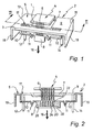
- FIG. 1 shows a carrier 2 and an electronic component 4 in the process of being assembled to the carrier.
- the component 4 is a liquid crystal display (LCD) 85 mm long, 40 mm wide and 2 mm thick.
- the LCD 4 is generally planar in shape and has a number of long, flexible, straight connection pins 6 that extend from near the centre of a straight front edge 1 of the LCD 4 in a direction perpendicular to the plane of the LCD.
- the carrier 2 has a generally planar top portion 5 with an upwardly facing surface 9 in which there is a centrally located recess 7 for receiving the LCD 4 in a snap-fit engagement. When LCD 4 is in engagement with the carrier 2, the LCD is flush with the planar top portion 5.
- the recess may include a back light (not shown) for illuminating the LCD 4.
- a pair of skirts 18, 19 project downwards perpendicularly to the plane of the LCD 4 from two opposite side edges 13, 15 of the planar top portion 5.
- a rectangular hole 17 is provided through the planar top portion 5 near and parallel to the front edge 3 of the planar top portion 5 to permit the LCD connection pins 6 to extend beneath the level of the upwardly facing surface when the LCD is engaged with the carrier 2. This movement is in the same direction as the length of the pins 6, and defines a connection axis 16. It should be understood that references to front and back refer only to the orientation of the carrier as shown in the drawings.
- a substantially rectangular pin guide 8 is suspended from the planar top portion 5 below the hole 17 and located centrally between the skirts 18,19 by a pair of intervening flexible portions 10.
- the flexible portions 10 extend from either side of the pin guide 8 in directions parallel to the front edge 3 of the planar top portion 5 and are attached near the front edge 3 at points on either side of the hole 17.
- the flexible portions 10 each have a zig-zag bend 11 either side of the pin guide 8 to aid flexing along the connection axis 16.
- the carrier 2 also has two spike-shaped locator devices 12,14 extending downwardly from the planar top portion 5 in a direction parallel to the connection axis 16. These locator devices 12,14 are positioned behind the flexible portions 10 and extend beyond the skirts 18,19.
- Figure 2 shows a schematic cross section view through the carrier 2 and the LCD 4 taken along the line II-II of Figure 1.
- the drawing shows the general shape of a number of channels 20 through the pin guide 8 and how each one of the pins 6 lines up with a corresponding one of the channels 20 when the LCD 4 is about to be assembled to the carrier along the connection axis.
- Each channel 20 has a funnel-shaped entrance 22 that is wider than the pin 6 to facilitate entry of the pin 6 into the channel 20.
- the recess 7 provides an easy way to approximately align the LCD 4 with the carrier 2 prior to assembly and thus allow the pins 6 to be aligned approximately with the channel entrances 22 prior to assembly.
- Each channel 20 narrows towards an exit 24 of the channel 20, the exit 24 being a clearance fit with the pin 6 such that each pin 6 is accurately positioned with respect to the pin guide 8 as each pin 6 approaches the corresponding pin guide exit 24, as shown in Figure 3.
- the pin guide 8 is rectangular in a cross-section parallel with the planar top portion 5, and has a similarly rectangular base 28 extending around the pin exits 24.
- the pin guide base 28 is surrounded on its four sides by a downwardly protruding rim 26.
- the rim extends in the direction of the connection axis 16.
- This protrusion 26 is shaped to provide a wide opening which narrows upwardly towards the pin guide base 28 to facilitate the location and engagement of the pin guide 8 with a matching receiving socket 42 as shown in Figures 4, 5 and 6.
- Figure 3 shows a cross section view similar to Figure 2, showing the LCD 4 assembled to the carrier 2, with the LCD 4 fully seated into the recess 17 in the planar top portion 5. This prevents movement of the component 4 relative to the carrier 2 and thus prevents damage to the pins 6, which are located within their respective channels 20.
- Figure 4 shows the assembly of carrier 2 and LCD 4 onto a circuit board 40 with the socket 42 mounted on the circuit board.
- the circuit board 40 is located below the carrier 2 and parallel to the plane of the LCD 4 and the planar top portion 5.
- the approximate location of the carrier 2 and the circuit board 40 is achieved by moving the carrier 2 and the circuit board 40 together along the connection axis 16.
- the spike-shaped locator devices 12,14 make contact first with the circuit board 40, and locate into respective matching holes 41 in the circuit board 40.
- the spiked shape of the locator devices 12,14 allows for some error in the alignment of the carrier 2 with the board 40 prior to full assembly.
- Figure 5 shows a further stage in the assembly of carrier 2 and LCD 4 to the circuit board 40.
- the accurate location of the pin guide 8 over the socket 42 has been achieved by the funnel-shaped protruding rim 26 on the pin guide locating the pin guide 8 over the socket 42 correctly.
- This alignment may include deflection of the flexible portions 10 to allow the pin guide 8 to move in directions transverse to the connection axis 16 so that the pin guide 8 may seat accurately over the socket 42.
- the pin exits 24 from the channels 20 align with the corresponding entrances 52 and connection holes 54 in the socket 42.
- Figure 6 shows the pins 6 fully inserted into the respective holes 54 in the socket 42. This has been achieved by the deflection of the flexible portion 10 of the component carrier 2 to allow the pin guide 8 to move in a direction along the connection axis 16 towards the planar top portion 5. This deflection is caused by a force applied to the pin guide 8 by the socket 42 in the direction of the connection axis 16.
- the skirts 18, 19 come into contact with the circuit board 40 and support the carrier 2 at a distance from the circuit board 40. This distance being sufficient to allow the pins 6 to enter the connection holes 54, but not be forced onto the circuit board 40 causing possible bending or damage.
- the distance is also sufficient to permit a conventional LCD backlight (not shown) to be provided on the board 40 or the carrier 2.
- barbs may be provided on the skirts 18,19, locator pins 12,14 or other parts, to effect a "snap-fit" to the circuit board.
- This allows the carrier 2 and LCD 4 to be held to the board securely.
- the "snap-fit” preferably also allows the carrier to be removed easily from the circuit board and replaced with another if it is, for instance, found to be faulty. This will reduce the need to scrap a circuit board with many components already attached simply because one component is found to be faulty.
Landscapes
- Engineering & Computer Science (AREA)
- Microelectronics & Electronic Packaging (AREA)
- Manufacturing & Machinery (AREA)
- Devices For Indicating Variable Information By Combining Individual Elements (AREA)
- Packaging Frangible Articles (AREA)
Abstract
Description
Claims (14)
- A carrier (2) for holding an electric component (4) having a one or more electrical connection pins (6), comprising a frame (7,9) for holding the component (4), a pin guide (8), and a flexible portion (10) connecting the pin guide (8) to the frame (7,9), wherein:a) the pin guide (8) has one or more channels (20) therethrough for receiving said electrical connection pins (6), the or each channel (20) extending along a connection axis (16);b) the frame (7,9) has a base (18,19) for mounting the carrier (2) to a surface that extends transverse to the connection axis (16);c) the flexible portion (10) is adapted to flex to allow the pin guide (8) to move parallel to the connection axis (16) when the pin guide (8) is pressed in a direction along the connection axis (16).
- An electronic assembly, comprising a carrier (2) and an electronic component (4) having one or more connection pins (6), the electronic component (4) being assembled to the carrier (2) and the carrier being as claimed in Claim 1, wherein the or each connection pin (6) extends into a corresponding channel (20) in the pin guide (8).
- An electronic assembly as claimed in Claim 2, in which: the or each channel (20) has an entrance (22) into which an end of the corresponding pin (6) is inserted when the electronic component (4) is assembled to the carrier (2), and an exit (24) from which the pin (6) protrudes when the pin guide (8) is moves along the connection axis (16); and the end of the pin (6) is protected within the channel (20) when the electronic component (4) is initially assembled to the carrier (2), and protrudes from the channel (20) when the pin guide (8) is moved along the connection axis (16).
- An electronic assembly as claimed in Claim 3, in which the pin guide (8) has one or more protrusions (26) that extend beyond the channel exit(s) (24) in the direction of the connection axis (16).
- An electronic assembly as claimed in Claim 3 or Claim 4, in which the entrance (22) to the channel (20) is funnel-shaped to aid insertion of the corresponding pin (6).
- An electronic assembly as claimed in any of Claims 2 to 5, in which the or each channel exit (24) has a clearance fit with the corresponding pin (6) to align the pin in orthogonal transverse directions to the connection axis (16) when said pin (6) protrudes from the exit (24).
- An electronic assembly as claimed in any of Claims 2 to 6, in which the flexible portion (10) is resiliently biased to a neutral position, and the end of the pin (6) is fully retained in the channel (20) when the flexible portion (10) is in the neutral position.
- An electronic assembly as claimed in any of Claims 2 to 4, in which the flexible portion (10) of the carrier (2) comprises a pair of arms (10) that extend generally transverse to the connection axis (16) in opposite directions from the frame (7,9) towards the pin guide (8).
- An electronic assembly as claimed in any of Claims 2 to 8, in which the electronic component is a planar display element (4) with one or more connection pins (6) extending from the element (4) in a direction transverse to the plane of the element.
- A circuit board assembly, comprising an electronic assembly (2,4) and a circuit board (40), the electronic assembly being mounted to the circuit board, and the electronic assembly being as claimed in any of Claims 2 to 9, wherein the or each connection pin (6) is electronically connected to a matching connection (54) on the circuit board (40).
- A circuit board assembly as claimed in Claim 10, including a socket (42), the socket being mounted on the circuit board (40) and having one or more pin receptacles (54), in which the shape of the pin guide (8) matches the shape of the socket (42) so that the or each pin (6) is automatically aligned with a corresponding pin receptacle (54) as the electronic assembly (2,4) is mounted to the circuit board (40).
- A circuit board assembly as claimed in Claim 10, in which the socket (42) protrudes from the circuit board (40), and the pin guide (8) has a recess (26) that matches the protrusion of the socket (42).
- A circuit board assembly as claimed in Claim 11 or Claim 12, in which the carrier (2) and circuit board (40) have an alignment means (12,14,41) by which the carrier (2) is brought into approximate alignment with the circuit board (40) as the electronic assembly (2,4) is mounted to the circuit board (40).
- A circuit board assembly as claimed in Claim 13, in which during mounting of the electronic assembly (2,4) to the circuit board (40), the approximate alignment is made before the pin guide (8) comes into contact with the socket (42).
Applications Claiming Priority (2)
| Application Number | Priority Date | Filing Date | Title |
|---|---|---|---|
| GB0105343A GB2372878B (en) | 2001-03-03 | 2001-03-03 | Component carrier |
| GB0105343 | 2001-03-03 |
Publications (3)
| Publication Number | Publication Date |
|---|---|
| EP1237396A2 true EP1237396A2 (en) | 2002-09-04 |
| EP1237396A3 EP1237396A3 (en) | 2004-01-07 |
| EP1237396B1 EP1237396B1 (en) | 2005-04-06 |
Family
ID=9909958
Family Applications (1)
| Application Number | Title | Priority Date | Filing Date |
|---|---|---|---|
| EP02250476A Expired - Lifetime EP1237396B1 (en) | 2001-03-03 | 2002-01-24 | Component carrier |
Country Status (4)
| Country | Link |
|---|---|
| US (1) | US6932637B2 (en) |
| EP (1) | EP1237396B1 (en) |
| DE (1) | DE60203556T2 (en) |
| GB (1) | GB2372878B (en) |
Families Citing this family (3)
| Publication number | Priority date | Publication date | Assignee | Title |
|---|---|---|---|---|
| CN102315531A (en) * | 2010-07-05 | 2012-01-11 | 鸿富锦精密工业(深圳)有限公司 | Electric connecting device and terminal thereof |
| US8721356B2 (en) * | 2012-09-11 | 2014-05-13 | Apple Inc. | Dock with compliant connector mount |
| CN109616810B (en) * | 2017-09-30 | 2021-01-29 | 中航光电科技股份有限公司 | A kind of interface unit |
Family Cites Families (14)
| Publication number | Priority date | Publication date | Assignee | Title |
|---|---|---|---|---|
| US3651444A (en) * | 1970-06-23 | 1972-03-21 | Amp Inc | Printed circuit board connector |
| US4227765A (en) * | 1979-02-12 | 1980-10-14 | Raytheon Company | Coaxial electrical connector |
| US4417777A (en) * | 1981-10-13 | 1983-11-29 | Molex Incorporated | Integrated circuit carrier assembly |
| CA1310693C (en) * | 1988-01-27 | 1992-11-24 | Manfred Prokopp | Electrical connecting apparatus for an electrical or electronic testing unit |
| US4954094A (en) * | 1989-09-15 | 1990-09-04 | Gte Products Corporation | Sliding gimbal connector |
| JP3107106B2 (en) * | 1991-12-13 | 2000-11-06 | ソニー株式会社 | Liquid crystal display |
| JPH06231833A (en) * | 1993-02-01 | 1994-08-19 | Fujitsu Ltd | Connector |
| JP3007812U (en) * | 1994-05-25 | 1995-02-28 | モレックス インコーポレーテッド | Surface mount electrical connector |
| JP3236775B2 (en) * | 1996-03-18 | 2001-12-10 | 株式会社オートネットワーク技術研究所 | Connector connection structure |
| GB2328329A (en) * | 1997-08-13 | 1999-02-17 | Ford Motor Co | Guiding pins for an electrical connection |
| US6224407B1 (en) * | 1997-12-17 | 2001-05-01 | The Whitaker Corporation | Coaxial switch connector assembly |
| DE29902762U1 (en) * | 1999-02-16 | 1999-04-29 | Samson Ag, 60314 Frankfurt | Spacers for display modules |
| US6592387B2 (en) * | 2000-12-22 | 2003-07-15 | Honeywell International Inc. | Spring-loaded connector setup for blind mating and method for using the same |
| US6390841B1 (en) * | 2001-04-25 | 2002-05-21 | Lear Corporation | Self-aligning electrical connector |
-
2001
- 2001-03-03 GB GB0105343A patent/GB2372878B/en not_active Expired - Fee Related
-
2002
- 2002-01-24 EP EP02250476A patent/EP1237396B1/en not_active Expired - Lifetime
- 2002-01-24 DE DE60203556T patent/DE60203556T2/en not_active Expired - Fee Related
- 2002-03-01 US US10/087,276 patent/US6932637B2/en not_active Expired - Fee Related
Also Published As
| Publication number | Publication date |
|---|---|
| DE60203556T2 (en) | 2006-03-16 |
| US6932637B2 (en) | 2005-08-23 |
| GB2372878B (en) | 2004-12-08 |
| DE60203556D1 (en) | 2005-05-12 |
| US20020146928A1 (en) | 2002-10-10 |
| EP1237396B1 (en) | 2005-04-06 |
| GB2372878A (en) | 2002-09-04 |
| EP1237396A3 (en) | 2004-01-07 |
| GB0105343D0 (en) | 2001-04-18 |
Similar Documents
| Publication | Publication Date | Title |
|---|---|---|
| KR970000130B1 (en) | Lcd cluster connector | |
| CN101320858B (en) | Connector | |
| KR950000431B1 (en) | Clamping contact element and edge connector made up of several of such clamping contact elements for the connection of conductor | |
| US6091474A (en) | Display assembly | |
| JP3967023B2 (en) | Display mounting connection device | |
| JP2015056233A (en) | Cable holding member, electrical connection device, connector device | |
| US4663695A (en) | Holding device for mounting an electronic component on a printed circuit board | |
| US4650267A (en) | Device for fixing electronic display | |
| US4987516A (en) | Substrate carrier device | |
| EP1237396B1 (en) | Component carrier | |
| US5653018A (en) | Method for the manufacture of an electric appliance | |
| US8795002B2 (en) | Co-edge connector | |
| EP3522305A1 (en) | On-board diagnostic system connector terminal and on-board diagnostic system | |
| JPH0556677B2 (en) | ||
| JP2003045525A (en) | connector | |
| CN100413148C (en) | Terminals for flat cables, electrical connectors and flat cables with electrical connectors | |
| US4936786A (en) | Automated connection for a vehicle radio | |
| US10305208B2 (en) | Electronic device | |
| EP1497893B1 (en) | Retainer bracket for connectors | |
| US6106322A (en) | Electrical connections | |
| CN223757806U (en) | A grooved bracket structure and a light-emitting connector | |
| JP2006210733A (en) | Electronic device having structure for reinforcing connection terminal | |
| JP2008292530A (en) | Thin display device | |
| JP3357597B2 (en) | LCD terminal positioning structure | |
| EP0997982A2 (en) | Electrical connector for printed circuit boards |
Legal Events
| Date | Code | Title | Description |
|---|---|---|---|
| PUAI | Public reference made under article 153(3) epc to a published international application that has entered the european phase |
Free format text: ORIGINAL CODE: 0009012 |
|
| AK | Designated contracting states |
Kind code of ref document: A2 Designated state(s): AT BE CH CY DE DK ES FI FR GB GR IE IT LI LU MC NL PT SE TR |
|
| AX | Request for extension of the european patent |
Free format text: AL;LT;LV;MK;RO;SI |
|
| PUAL | Search report despatched |
Free format text: ORIGINAL CODE: 0009013 |
|
| AK | Designated contracting states |
Kind code of ref document: A3 Designated state(s): AT BE CH CY DE DK ES FI FR GB GR IE IT LI LU MC NL PT SE TR |
|
| AX | Request for extension of the european patent |
Extension state: AL LT LV MK RO SI |
|
| 17P | Request for examination filed |
Effective date: 20040227 |
|
| GRAP | Despatch of communication of intention to grant a patent |
Free format text: ORIGINAL CODE: EPIDOSNIGR1 |
|
| AKX | Designation fees paid |
Designated state(s): DE FR GB |
|
| RBV | Designated contracting states (corrected) |
Designated state(s): DE FR GB PT |
|
| RBV | Designated contracting states (corrected) |
Designated state(s): DE FR PT |
|
| GRAS | Grant fee paid |
Free format text: ORIGINAL CODE: EPIDOSNIGR3 |
|
| GRAA | (expected) grant |
Free format text: ORIGINAL CODE: 0009210 |
|
| AK | Designated contracting states |
Kind code of ref document: B1 Designated state(s): DE FR PT |
|
| REG | Reference to a national code |
Ref country code: IE Ref legal event code: FG4D |
|
| REF | Corresponds to: |
Ref document number: 60203556 Country of ref document: DE Date of ref document: 20050512 Kind code of ref document: P |
|
| RIN2 | Information on inventor provided after grant (corrected) |
Inventor name: GUIRAUTON, PASCAL Inventor name: MANGAT, RAPINDER Inventor name: EWERS, PAUL SIMON |
|
| PG25 | Lapsed in a contracting state [announced via postgrant information from national office to epo] |
Ref country code: PT Free format text: LAPSE BECAUSE OF FAILURE TO SUBMIT A TRANSLATION OF THE DESCRIPTION OR TO PAY THE FEE WITHIN THE PRESCRIBED TIME-LIMIT Effective date: 20050908 |
|
| PLBE | No opposition filed within time limit |
Free format text: ORIGINAL CODE: 0009261 |
|
| STAA | Information on the status of an ep patent application or granted ep patent |
Free format text: STATUS: NO OPPOSITION FILED WITHIN TIME LIMIT |
|
| 26N | No opposition filed |
Effective date: 20060110 |
|
| EN | Fr: translation not filed | ||
| PG25 | Lapsed in a contracting state [announced via postgrant information from national office to epo] |
Ref country code: FR Free format text: LAPSE BECAUSE OF FAILURE TO SUBMIT A TRANSLATION OF THE DESCRIPTION OR TO PAY THE FEE WITHIN THE PRESCRIBED TIME-LIMIT Effective date: 20050406 |
|
| PGFP | Annual fee paid to national office [announced via postgrant information from national office to epo] |
Ref country code: DE Payment date: 20090122 Year of fee payment: 8 |
|
| PG25 | Lapsed in a contracting state [announced via postgrant information from national office to epo] |
Ref country code: DE Free format text: LAPSE BECAUSE OF NON-PAYMENT OF DUE FEES Effective date: 20100803 |