EP1237185A3 - A method for manufacturing isolating structures - Google Patents
A method for manufacturing isolating structures Download PDFInfo
- Publication number
- EP1237185A3 EP1237185A3 EP02003714A EP02003714A EP1237185A3 EP 1237185 A3 EP1237185 A3 EP 1237185A3 EP 02003714 A EP02003714 A EP 02003714A EP 02003714 A EP02003714 A EP 02003714A EP 1237185 A3 EP1237185 A3 EP 1237185A3
- Authority
- EP
- European Patent Office
- Prior art keywords
- silicon carbide
- layer
- carbide layer
- isolating structures
- thickness
- Prior art date
- Legal status (The legal status is an assumption and is not a legal conclusion. Google has not performed a legal analysis and makes no representation as to the accuracy of the status listed.)
- Withdrawn
Links
Classifications
-
- H—ELECTRICITY
- H10—SEMICONDUCTOR DEVICES; ELECTRIC SOLID-STATE DEVICES NOT OTHERWISE PROVIDED FOR
- H10W—GENERIC PACKAGES, INTERCONNECTIONS, CONNECTORS OR OTHER CONSTRUCTIONAL DETAILS OF DEVICES COVERED BY CLASS H10
- H10W10/00—Isolation regions in semiconductor bodies between components of integrated devices
- H10W10/01—Manufacture or treatment
- H10W10/011—Manufacture or treatment of isolation regions comprising dielectric materials
- H10W10/014—Manufacture or treatment of isolation regions comprising dielectric materials using trench refilling with dielectric materials, e.g. shallow trench isolations
-
- H—ELECTRICITY
- H10—SEMICONDUCTOR DEVICES; ELECTRIC SOLID-STATE DEVICES NOT OTHERWISE PROVIDED FOR
- H10W—GENERIC PACKAGES, INTERCONNECTIONS, CONNECTORS OR OTHER CONSTRUCTIONAL DETAILS OF DEVICES COVERED BY CLASS H10
- H10W10/00—Isolation regions in semiconductor bodies between components of integrated devices
- H10W10/01—Manufacture or treatment
-
- H—ELECTRICITY
- H10—SEMICONDUCTOR DEVICES; ELECTRIC SOLID-STATE DEVICES NOT OTHERWISE PROVIDED FOR
- H10W—GENERIC PACKAGES, INTERCONNECTIONS, CONNECTORS OR OTHER CONSTRUCTIONAL DETAILS OF DEVICES COVERED BY CLASS H10
- H10W10/00—Isolation regions in semiconductor bodies between components of integrated devices
- H10W10/10—Isolation regions comprising dielectric materials
- H10W10/17—Isolation regions comprising dielectric materials formed using trench refilling with dielectric materials, e.g. shallow trench isolations
Landscapes
- Element Separation (AREA)
- Formation Of Insulating Films (AREA)
- Drying Of Semiconductors (AREA)
- Processing Of Terminals (AREA)
Abstract
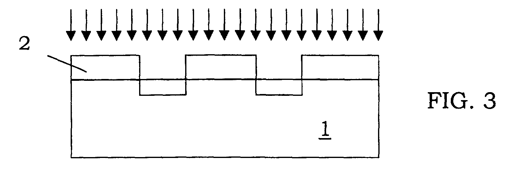
- depositing a masking layer (2) onto the silicon carbide layer (1,8); and
- forming openings (2a) through said masking layer (2) to expose
portions of the silicon carbide layer (1,8); and further comprises the
steps of:
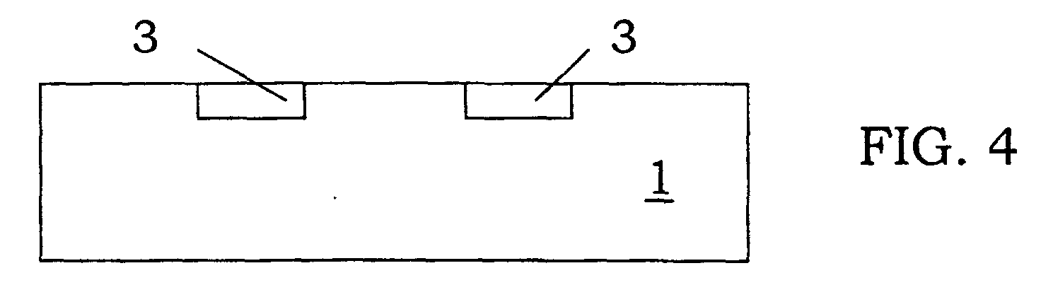
- ion implanting the whole chip surface;
- heat treating the entire surface of the silicon carbide layer (1,8) to form an oxide layer (4) having a first portion (5) with a first thickness in said at least one region (3), and having a second portion (6) with a second thickness at said silicon carbide layer (1,8).
Applications Claiming Priority (2)
| Application Number | Priority Date | Filing Date | Title |
|---|---|---|---|
| IT2001MI000339A ITMI20010339A1 (en) | 2001-02-20 | 2001-02-20 | METHOD TO CREATE INSULATING STRUCTURES |
| ITMI010339 | 2001-02-20 |
Publications (2)
| Publication Number | Publication Date |
|---|---|
| EP1237185A2 EP1237185A2 (en) | 2002-09-04 |
| EP1237185A3 true EP1237185A3 (en) | 2003-07-30 |
Family
ID=11446939
Family Applications (1)
| Application Number | Title | Priority Date | Filing Date |
|---|---|---|---|
| EP02003714A Withdrawn EP1237185A3 (en) | 2001-02-20 | 2002-02-19 | A method for manufacturing isolating structures |
Country Status (3)
| Country | Link |
|---|---|
| US (1) | US6762112B2 (en) |
| EP (1) | EP1237185A3 (en) |
| IT (1) | ITMI20010339A1 (en) |
Families Citing this family (8)
| Publication number | Priority date | Publication date | Assignee | Title |
|---|---|---|---|---|
| FR2888665B1 (en) * | 2005-07-18 | 2007-10-19 | St Microelectronics Crolles 2 | METHOD FOR PRODUCING A MOS TRANSISTOR AND CORRESPONDING INTEGRATED CIRCUIT |
| US7808029B2 (en) * | 2006-04-26 | 2010-10-05 | Siliconix Technology C.V. | Mask structure for manufacture of trench type semiconductor device |
| US8084811B2 (en) * | 2009-10-08 | 2011-12-27 | Monolithic Power Systems, Inc. | Power devices with super junctions and associated methods manufacturing |
| US20150050358A1 (en) * | 2013-08-15 | 2015-02-19 | Regents Of The University Of Minnesota | Implant support composition and methods of use |
| US10727649B2 (en) * | 2018-09-21 | 2020-07-28 | Argo AI, LLC | Monolithic series-connected edge-emitting-laser array and method of fabrication |
| EP3800660B1 (en) | 2019-10-02 | 2025-02-19 | STMicroelectronics S.r.l. | Silicon carbide power device with improved robustness and corresponding manufacturing process |
| CN216413051U (en) | 2020-09-04 | 2022-04-29 | 意法半导体股份有限公司 | semiconductor equipment |
| JP7758501B2 (en) | 2020-09-04 | 2025-10-22 | エスティーマイクロエレクトロニクス エス.アール.エル. | Method for manufacturing elements of electronic devices with improved reliability, and related elements, electronic devices, and electronic equipment |
Citations (2)
| Publication number | Priority date | Publication date | Assignee | Title |
|---|---|---|---|---|
| EP0363944A1 (en) * | 1988-10-12 | 1990-04-18 | Fujitsu Limited | Method of manufacturing a semiconductor device having a silicon carbide layer |
| EP0845803A1 (en) * | 1996-04-18 | 1998-06-03 | Matsushita Electric Industrial Co., Ltd | SiC ELEMENT AND PROCESS FOR ITS PRODUCTION |
Family Cites Families (1)
| Publication number | Priority date | Publication date | Assignee | Title |
|---|---|---|---|---|
| US5270244A (en) * | 1993-01-25 | 1993-12-14 | North Carolina State University At Raleigh | Method for forming an oxide-filled trench in silicon carbide |
-
2001
- 2001-02-20 IT IT2001MI000339A patent/ITMI20010339A1/en unknown
-
2002
- 2002-02-19 EP EP02003714A patent/EP1237185A3/en not_active Withdrawn
- 2002-02-20 US US10/079,925 patent/US6762112B2/en not_active Expired - Lifetime
Patent Citations (2)
| Publication number | Priority date | Publication date | Assignee | Title |
|---|---|---|---|---|
| EP0363944A1 (en) * | 1988-10-12 | 1990-04-18 | Fujitsu Limited | Method of manufacturing a semiconductor device having a silicon carbide layer |
| EP0845803A1 (en) * | 1996-04-18 | 1998-06-03 | Matsushita Electric Industrial Co., Ltd | SiC ELEMENT AND PROCESS FOR ITS PRODUCTION |
Also Published As
| Publication number | Publication date |
|---|---|
| US20030003680A1 (en) | 2003-01-02 |
| EP1237185A2 (en) | 2002-09-04 |
| ITMI20010339A1 (en) | 2002-08-20 |
| US6762112B2 (en) | 2004-07-13 |
Similar Documents
| Publication | Publication Date | Title |
|---|---|---|
| EP1365447A3 (en) | Manufacturing method of semiconductor substrate | |
| WO2000014797A3 (en) | Isolation region forming methods | |
| EP1069605A3 (en) | Method for fabricating a semiconductor structure including a metal oxide interface with silicon | |
| EP0964436A3 (en) | Method for manufacturing SOI wafer and SOI wafer | |
| EP0905756A3 (en) | Planarization of a non-conformal device layer in semiconductor fabrication | |
| TW358236B (en) | Improved local silicon oxidization method in the manufacture of semiconductor isolation | |
| EP1022771A3 (en) | Improved contact and deep trench patterning | |
| WO2005050716A3 (en) | High-temperature devices on insulator substrates | |
| EP0977255A3 (en) | A method of fabricating an SOI wafer and SOI wafer fabricated by the method | |
| EP1164637A3 (en) | Method of making metallization and contact structures in an integrated circuit comprising an etch stop layer | |
| EP1115153A3 (en) | Semiconductor substrate and process for its production | |
| EP1014440A3 (en) | Area array air gap structure for intermetal dielectric application | |
| EP1398829A3 (en) | Substrate and manufacturing method therefor | |
| EP0908938A3 (en) | Buffer layer for improving control of layer thickness | |
| EP1139693A3 (en) | Ceramic heater and method for manufacturing the same | |
| WO2003034484A3 (en) | A method for forming a layered semiconductor structure and corresponding structure | |
| EP2378544A3 (en) | Semiconductor device fabricating method | |
| EP1237185A3 (en) | A method for manufacturing isolating structures | |
| TW368727B (en) | Manufacturing method for shallow trench isolation structure | |
| EP0999584A3 (en) | Method for manufacturing semiconductor device | |
| EP0908941A3 (en) | Deposition of carbon into nitride layer for improved selectivity of oxide to nitride etchrate for self aligned contact etching | |
| EP0997996A3 (en) | Semiconductor device and method for fabricating the same | |
| EP0391561A3 (en) | Forming wells in semiconductor devices | |
| EP0971424A3 (en) | Spin-valve structure and method for making spin-valve structures | |
| WO2003024711A3 (en) | Method for producing a ceramic substrate and ceramic substrate |
Legal Events
| Date | Code | Title | Description |
|---|---|---|---|
| PUAI | Public reference made under article 153(3) epc to a published international application that has entered the european phase |
Free format text: ORIGINAL CODE: 0009012 |
|
| AK | Designated contracting states |
Kind code of ref document: A2 Designated state(s): AT BE CH CY DE DK ES FI FR GB GR IE IT LI LU MC NL PT SE TR |
|
| AX | Request for extension of the european patent |
Free format text: AL;LT;LV;MK;RO;SI |
|
| PUAL | Search report despatched |
Free format text: ORIGINAL CODE: 0009013 |
|
| AK | Designated contracting states |
Designated state(s): AT BE CH CY DE DK ES FI FR GB GR IE IT LI LU MC NL PT SE TR |
|
| AX | Request for extension of the european patent |
Extension state: AL LT LV MK RO SI |
|
| 17P | Request for examination filed |
Effective date: 20040112 |
|
| AKX | Designation fees paid |
Designated state(s): DE FR GB IT |
|
| 17Q | First examination report despatched |
Effective date: 20041019 |
|
| STAA | Information on the status of an ep patent application or granted ep patent |
Free format text: STATUS: THE APPLICATION IS DEEMED TO BE WITHDRAWN |
|
| 18D | Application deemed to be withdrawn |
Effective date: 20050728 |