EP1235469A2 - Circuit board construction for differential bus distribution - Google Patents
Circuit board construction for differential bus distribution Download PDFInfo
- Publication number
- EP1235469A2 EP1235469A2 EP01123466A EP01123466A EP1235469A2 EP 1235469 A2 EP1235469 A2 EP 1235469A2 EP 01123466 A EP01123466 A EP 01123466A EP 01123466 A EP01123466 A EP 01123466A EP 1235469 A2 EP1235469 A2 EP 1235469A2
- Authority
- EP
- European Patent Office
- Prior art keywords
- trace
- field
- connector
- fields
- board
- Prior art date
- Legal status (The legal status is an assumption and is not a legal conclusion. Google has not performed a legal analysis and makes no representation as to the accuracy of the status listed.)
- Withdrawn
Links
Images





Classifications
-
- H—ELECTRICITY
- H05—ELECTRIC TECHNIQUES NOT OTHERWISE PROVIDED FOR
- H05K—PRINTED CIRCUITS; CASINGS OR CONSTRUCTIONAL DETAILS OF ELECTRIC APPARATUS; MANUFACTURE OF ASSEMBLAGES OF ELECTRICAL COMPONENTS
- H05K1/00—Printed circuits
- H05K1/02—Details
- H05K1/0213—Electrical arrangements not otherwise provided for
- H05K1/0216—Reduction of cross-talk, noise or electromagnetic interference
- H05K1/0228—Compensation of cross-talk by a mutually correlated lay-out of printed circuit traces, e.g. for compensation of cross-talk in mounted connectors
-
- H—ELECTRICITY
- H05—ELECTRIC TECHNIQUES NOT OTHERWISE PROVIDED FOR
- H05K—PRINTED CIRCUITS; CASINGS OR CONSTRUCTIONAL DETAILS OF ELECTRIC APPARATUS; MANUFACTURE OF ASSEMBLAGES OF ELECTRICAL COMPONENTS
- H05K1/00—Printed circuits
- H05K1/02—Details
- H05K1/14—Structural association of two or more printed circuits
-
- H—ELECTRICITY
- H01—ELECTRIC ELEMENTS
- H01R—ELECTRICALLY-CONDUCTIVE CONNECTIONS; STRUCTURAL ASSOCIATIONS OF A PLURALITY OF MUTUALLY-INSULATED ELECTRICAL CONNECTING ELEMENTS; COUPLING DEVICES; CURRENT COLLECTORS
- H01R12/00—Structural associations of a plurality of mutually-insulated electrical connecting elements, specially adapted for printed circuits, e.g. printed circuit boards [PCB], flat or ribbon cables, or like generally planar structures, e.g. terminal strips, terminal blocks; Coupling devices specially adapted for printed circuits, flat or ribbon cables, or like generally planar structures; Terminals specially adapted for contact with, or insertion into, printed circuits, flat or ribbon cables, or like generally planar structures
- H01R12/70—Coupling devices
- H01R12/71—Coupling devices for rigid printing circuits or like structures
- H01R12/712—Coupling devices for rigid printing circuits or like structures co-operating with the surface of the printed circuit or with a coupling device exclusively provided on the surface of the printed circuit
-
- H—ELECTRICITY
- H05—ELECTRIC TECHNIQUES NOT OTHERWISE PROVIDED FOR
- H05K—PRINTED CIRCUITS; CASINGS OR CONSTRUCTIONAL DETAILS OF ELECTRIC APPARATUS; MANUFACTURE OF ASSEMBLAGES OF ELECTRICAL COMPONENTS
- H05K1/00—Printed circuits
- H05K1/02—Details
- H05K1/11—Printed elements for providing electric connections to or between printed circuits
- H05K1/115—Via connections; Lands around holes or via connections
-
- H—ELECTRICITY
- H05—ELECTRIC TECHNIQUES NOT OTHERWISE PROVIDED FOR
- H05K—PRINTED CIRCUITS; CASINGS OR CONSTRUCTIONAL DETAILS OF ELECTRIC APPARATUS; MANUFACTURE OF ASSEMBLAGES OF ELECTRICAL COMPONENTS
- H05K2201/00—Indexing scheme relating to printed circuits covered by H05K1/00
- H05K2201/09—Shape and layout
- H05K2201/09209—Shape and layout details of conductors
- H05K2201/09218—Conductive traces
- H05K2201/09236—Parallel layout
-
- H—ELECTRICITY
- H05—ELECTRIC TECHNIQUES NOT OTHERWISE PROVIDED FOR
- H05K—PRINTED CIRCUITS; CASINGS OR CONSTRUCTIONAL DETAILS OF ELECTRIC APPARATUS; MANUFACTURE OF ASSEMBLAGES OF ELECTRICAL COMPONENTS
- H05K2201/00—Indexing scheme relating to printed circuits covered by H05K1/00
- H05K2201/09—Shape and layout
- H05K2201/09209—Shape and layout details of conductors
- H05K2201/09218—Conductive traces
- H05K2201/09245—Crossing layout
-
- H—ELECTRICITY
- H05—ELECTRIC TECHNIQUES NOT OTHERWISE PROVIDED FOR
- H05K—PRINTED CIRCUITS; CASINGS OR CONSTRUCTIONAL DETAILS OF ELECTRIC APPARATUS; MANUFACTURE OF ASSEMBLAGES OF ELECTRICAL COMPONENTS
- H05K2201/00—Indexing scheme relating to printed circuits covered by H05K1/00
- H05K2201/09—Shape and layout
- H05K2201/09209—Shape and layout details of conductors
- H05K2201/09654—Shape and layout details of conductors covering at least two types of conductors provided for in H05K2201/09218 - H05K2201/095
- H05K2201/09709—Staggered pads, lands or terminals; Parallel conductors in different planes
-
- H—ELECTRICITY
- H05—ELECTRIC TECHNIQUES NOT OTHERWISE PROVIDED FOR
- H05K—PRINTED CIRCUITS; CASINGS OR CONSTRUCTIONAL DETAILS OF ELECTRIC APPARATUS; MANUFACTURE OF ASSEMBLAGES OF ELECTRICAL COMPONENTS
- H05K2201/00—Indexing scheme relating to printed circuits covered by H05K1/00
- H05K2201/10—Details of components or other objects attached to or integrated in a printed circuit board
- H05K2201/10007—Types of components
- H05K2201/10189—Non-printed connector
Definitions
- the invention relates generally to improvements in circuit boards useful for supporting and interconnecting computer devices, such as disk drives and processors. More specifically, the invention pertains to multi-layered circuit boards including differential buses and special via fields, to provide high speed signal transfers between and among electronic devices.
- Modern computer systems use high speed digital buses to connect high performance computer devices, such as disk drives and processors.
- these buses comprise a plurality of parallel, conductive wires or traces.
- the bus wires are typically arranged on a printed circuit board, which may have inner or outer traces of bus wires separated by non-conductive core material.
- Active terminating loads designed to match trace characteristic impedances, are provided at the end of each wire or trace. These loads include a load resistor, and may also include a voltage source or a current source.
- the computer devices are connected to traces in the intermediate portion of the bus by means of wire stubs.
- the wire stubs extend across the bus, providing a parallel electrical connection for the transversely positioned device. Because stubs are transverse to the bus, stubs introduce signal perturbations and noise artifacts into the data transmitted through the bus of the computer system.
- stubs creates other problems in the design of circuit board layouts. It is typical to plug the computer devices into connectors or sockets, mounted to the printed circuit board. The stubs or other connection traces lead from the pins of the connectors to the bus. As the complexity of the computer system increases, the number of devices which must be connected to the bus also increases. However with a greater number of devices to mount on the board and to interconnect to the bus, the circuit layout of the board becomes increasingly difficult to implement. The long, parallel traces between devices must be routed to maintain a specific trace impedance, minimize crosstalk, minimize consumption of circuit board space, equalize the trace lengths, and use the least number of board layers. As a result, compromises are made in the performance of the computer system, so that all the devices can be interconnected as required.
- Buses used for interconnecting devices may be either of single-ended or differential design
- Single-ended buses rely upon circuits comprised of a plurality of single conductors, spaced and insulated from a ground plane which is common to all conductors.
- single-ended buses are relatively easy to implement, they have significant limitations in data transfer rates, and are subject to adjacent channel noise interference, as well.
- Differential buses in contrast, use a pair of conductors, or trace-pairs, arranged in spaced relation and insulated from a ground plane.
- the predetermined spacing between the two conductors in conjunction with the insulating dielectric and the ground plane, provide a controlled impedance layer for the rapid and efficient transfer of digital data.
- Both of the conductors are electrically above the ground plane at all times.
- Transmitters and receivers are employed at each end of the trace-pairs to encode and decode a predetermined signal differential between them. Consequently, differential buses provide the advantages of increased data rate transfer and greater immunity from noise, when compared to single-ended buses. However, because differential buses require two traces, they further restrain the options for circuit board layout and design.
- the apparatus of the present invention employs a four-layered printed circuit board, for the purpose of mounting and electrically interconnecting two or more computer devices.
- These devices may include disk drives, processors, and external cables.
- Each of these devices is adapted to plug into a conventional device connector, such as a four row, twenty column SCSI (Small Computer System Interface) disk drive connector.
- the connectors may be located where desired on either side of the circuit board, for example, in a line along one edge, or on opposing edges of the board.
- Each connector includes at least one connector trace field, for connection to a differential bus. If the connector is to be connected to two connectors, then it includes two connector trace fields.
- the connector trace field provides a conductive transition between the pins of the connector and the bus.
- the differential bus is comprised of a plurality of trace-pairs of conductors, extending between adjacent computer devices. The first length of the differential bus is on a top side of the board, and the second length of the bus is on the bottom side of the board.
- a via trace field is provided to interconnect the first and second lengths of the bus.
- the via trace field includes a top via field and a bottom via field. These via trace fields are substantially identical in configuration and size to the conductor trace fields. Vias, providing a conductive path through the circuit board, interconnect the top and the bottom via fields.
- the via trace fields may include slight undulations so as to equalize the overall lengths of the trace-pairs in each differential bus.
- the via trace fields are also used selectively to reverse the trace or conductor order of groups of the trace-pairs, so that induced currents between the traces will cancel, minimizing crosstalk between them. This trace order reversal feature is also employed in the connector trace fields, to minimize crosstalk in an identical fashion.
- the via fields may be oriented parallel with respect to collinearly arranged devices, or orthogonal with respect to devices or connectors which are parallel. Where a connector has laterally offset groups of pin connections, a via field may also include offset groups of vias to provide trace length equalization. These orthogonally oriented via fields also have the capability of equaling the lengths of the buses, and reversing the conductor order of the traces within the buses, to ensure the integrity of signal transfer between computer devices.
- the trace-pairs are on the outside layers of the board, and the ground planes for each set of trace-pairs are buried in the board.
- the trace-pairs are buried in the board, and the outer board surfaces are ground planes
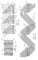
- Figure 1 shows the most basic form of an apparatus 11, designed to support and interconnect computer devices 12 and 13.
- devices 12 and 13 are only shown in broken outline form, each respectively overlying and plugged into, a first device connector 14 and a second device connector 16.
- Devices 12 and 13 may be any computer device, such as a disk drive or a processor.
- the connectors 14 and 16 may be of any appropriate type for the application, but in this case, the connectors are removable, wide SCSI disk drive connectors, including an array of pin connections which is four rows high and twenty columns wide.
- the elongated connectors are mounted with their axes aligned, along one edge of a four-layered circuit board 17. It should be noted that the connectors may also be arranged in parallel relation, as will be discussed in more detail herein. In addition, the connectors may be used either for computer devices or for cable connections, as needs dictate.
- Circuit board 17 known in the trade as a microstrip construction, is shown in a detailed cross-section, in Figure 5.
- Board 17 has a top side 18 and a bottom side 19, made from "prepreg", apreimpregnated dielectric material which has heat-activated adhesive properties.
- a top differential trace-pair 21 includes individual top traces 22 and 23, both arranged in spaced relation on top side 18.
- a conductive ground plane 24 Immediately below top side 18 is a conductive ground plane 24.
- a core 25, also made from a dielectric material, is provided in the center of the board 17. This basic combination of elements is the building block of the differential bus used for interconnections throughout the apparatus 11 of the present invention.
- a bottom differential trace-pair 26 is provided, which includes individual bottom traces 27 and 28.
- a conductive ground plane 29 is positioned above bottom side 19.
- a first connector trace field 31 is interconnected to connector 14 and a second connector trace field 32 is interconnected to connector 16.
- Trace field 31 includes a plurality of top trace-pairs 21 which are variously connected to "negative" pins 33 and "positive" pins 34.
- the negative signs and positive signs on the left hand side of Figure 7 are included to identify the polarities of particular pin rows. By following these pin polarities in conjunction with the respective trace lines leading from the pins, the subsequent explanation of the reversal of conductor, or trace order will be more clear.
- pin connection order "A" for a particular trace pair, corresponds to a "negative" pin connection for the left hand trace, and a "positive" pin connection for the right hand trace.
- pin connection order "B” corresponds to a "positive” pin connection for the left hand trace and a "negative” pin connection for the right hand trace. It will be appreciated, then, that first connector trace field 31 displays a repetitive, conductor order pattern of AABB.
- FIG 8 a different conductor order pattern is shown for the second connector trace field 32.
- trace field 32 is located on the bottom side 19 of circuit board 17.
- the trace-pairs of field 32 are shown in broken line in Figures 1 and 8.
- the connector pins 33 and 34 are respectively marked as negative and positive. Proceeding from the upper left hand side of trace field 32 to the right, it is evident that a conductor order pattern of ABBA pattern is employed.
- a via trace field 36 Interposed between the first connector 14 and the second connector 16 is a via trace field 36.
- One of the primary functions of the via field 36 is to effect a "fold-over" between two lengths of the differential bus. "Fold-over” refers to the corrective re-orientation of trace-pairs within a bus, so that pin connections between adjacent devices will be proper and symmetrical.
- the via trace field 36 has an orientation which is parallel to the axis of the collinearly aligned connectors 14 and 16. As will be shown herein, other orientations for the via field may be used as well, depending upon the location and the orientation of the connectors to be interconnected.
- via trace field 36 includes a top via field 37 and a bottom via field 38.
- Each ofthe trace-pairs in the top and bottom via fields is connected at one end to a respective via 39.
- the top via field 37 is connected to the vias 39 using the AABB conductor order pattern. This is the same conductor order pattern used by the first connector trace field 31.
- the bottom via field 3 8 is connected to the vias 39 using the ABBA conductor order pattern. This is the same conductor order pattern used by the second connector trace field 32.
- the twenty-seven pairs of vias 39 pass through the circuit board 17, and provide a conductive path between the top and bottom via trace fields.
- different conductor order patterns in the trace-pairs may be effected, at the same time the differential bus is undergoing a "fold-over".
- the top and bottom via trace fields 37 and 38 are substantially identical in size and configuration to the first and second connector trace fields 31 and 32.
- the number and the pattern of the vias 39 closely mirror the arrangement of the negative pins 33 and the positive pins 34 in the connectors 14 and 16.
- This general symmetry in trace field configurations and in pin and via arrangements provides a uniform and complementary transformation for the differential bus as it passes between connectors.
- the small undulations in the trace paths provide an opportunity to make adjustments in the overall lengths of each trace.
- the selective routing of trace paths through the via field provides a first mechanism through which the overall lengths of trace-paths in the bus can be equalized.
- first bus length 41 angles upwardly and to the right in a first path, then extends horizontally and to the right in a second path, and finally angles upwardly and to the right again in a third path.
- a plurality of bottom differential trace-pairs 26, comprising a second bus length 42 extends over the bottom side 19 of the board, between second connector trace field 32 and bottom via field 38.
- Second bus length angles upwardly and to the left in a first segment, then extends horizontally and to the left in a second segment, and lastly angles upwardly and to the left again in a third segment.
- first and the second lengths of the bus cross over or under each other, they are orthogonal to each other (see, Figures 1 and 9).
- Such an orientation inherently reduces crosstalk between channels, as the magnetic fields produced by the top and bottom traces are perpendicular to each other.
- this orientation reduces the proximal cross-over areas for the traces, minimizing capacitive coupling between the top and bottom traces.
- Top trace-pairs 21 are organized with a trace-pair conductor order of AABB.
- pattern A the "negative" trace is routed to the left and the "positive" trace is routed to the right.
- pattern B the order is reversed.
- stray capacitance and magnetic coupling between the positive trace of the first pair (pattern A) and the negative trace of the second pair (also pattern A) will cause crosstalk.
- the positive conductor of the first trace-pair (culprit trace) will impart a positive perturbation on the negative member of the second trace- pair (victim trace). An identical influence will be caused between the third and fourth pairs, arranged in pattern BB.
- the pattern of the same first, second, third, and fourth pairs is rearranged to ABBA.
- the same positive signal transition referenced above will cause an equal perturbation of the same polarity on the positive member of the second trace-pair on the bottom side of the board.
- the positive conductor of the first pair is still the culprit trace, but the now adjacent positive trace of the second pair is a new victim trace.
- both traces of the second pair will carry the same perturbation with the same polarity.
- the perturbation on the second pair is common-mode only. As a consequence of removing the differential component of the perturbation, the differential receivers of devices coupled to the bus do not respond to the perturbation.
- the culprit trace-pair remains with pattern A on both the top and the bottom of the circuit board.
- the victim trace-pair exchanges conductor order from the top side (pattern A) to the bottom side (pattern B).
- a different perturbation neutralization process occurs when the culprit trace-pair changes patterns and the victim trace pair retains the same conductor order. This circumstance arises from electro-magnetic interaction between the second and the third trace-pairs.
- the positive conductor of the second trace-pair (the culprit trace) will impart a positive perturbation on the positive conductor of the third trace- pair (the victim trace).
- the negative conductor of the second pair now becomes the new culprit trace, inducing a negative perturbation on the same positive victim trace of the third trace-pair.
- an equal and opposite perturbation on the second length of the bus cancels the initial perturbation imparted on the first length of the bus. In this case, the perturbation is completely canceled, leaving no differential or common mode components.
- the mechanisms for crosstalk neutralization employed in the apparatus 11 are similar to the mechanism which cancels crosstalk in twisted pairs of wires within a bundled cable.
- a bundled cable In a bundled cable, there is a random distribution of twists between adjacent twisted pairs.
- the likelihood of a twisted pair inducing signal perturbations more in one polarity than the other diminishes to an acceptable level. In other words, the totality of coupled perturbations of opposite twisted pair members approximately cancels.
- the method of cancellation employed in the present invention is somewhat different, in that traces on a printed circuit board, rather than bundles of twisted pairs of wires, are the circuit conductors.
- the method of cancellation used herein in somewhat more effective, as the symmetrical circuit topology coupled with the selective reversal of conductor ordering provides precisely opposing trace-pair influences in the differential bus extending between adjacent devices.
- Prior art circuit board arrangements do not exhibit the same efficiency and versatility for arranging computer devices on a circuit board, without compromising the circuit's immunity from crosstalk.
- a prior art bus arrangement 43 is shown, in which the connectors 44 of the computer devices are mounted directly over and connected to the parallel bus traces 46. Although this provides very straightforward routing for the bus traces, it is limited in use to circumstances where the computer devices may be vertically oriented.
- bus traces must follow a sinuous path in and around the device connectors to maintain the same pin sequence.
- This prior art bus arrangement 47 is shown in Figure 3.
- the device connectors 48 are mounted with their axes horizontal, and collinearly aligned.
- the bus 49 must undergo a 180 degree re-orientation path, which consumes a considerable amount of circuit board space on both sides of the connectors. In addition, it prevents the device connectors from being mounted along the edge of the circuit board.
- FIG 4 yet another prior art bus arrangement 51 is shown.
- the parallel bus 52 is located on the bottom side of the board (not shown). Bus 52 is therefore illustrated in broken line.
- Each device connector 53 is interconnected to the bus 52 by means of a respective stub 54.
- Arrangement 51 accomplishes bus "fold-over" by using both sides of the circuit board, and vias 56 passing through the circuit board, to connect the end of the stubs 54 with the bus 52.
- stubs create signal reflections in the bus, as the stubs are not properly terminated with a load and they are oriented transversely with respect to the bus.
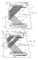
- FIG 11 an example of a via field 57 being oriented orthogonally with respect to parallel connectors 58 and 59, is shown.
- Connectors 58 and 59 may accept two computer devices, a computer device and a cable, or two cables.
- the connectors 58 and 59 are mounted with their axes offset, in parallel relation, along opposing upper and lower edges of a circuit board 17.
- a differential bus 61 including a plurality of trace pairs, interconnects connectors 58 and 59.
- Via field 57 is identical in construction to via field 36, described previously. However, owing to its orientation with respect to the axes of the connectors 58 and 59, the via field 57 is not in the center of each of the trace-pairs within bus 61.
- a top trace run 62 extends downwardly and to the left, from connector 59 to via field 57. Top trace run 62 lies over the top side 18 of circuit board 17.
- a bottom trace run 63 extends downwardly and to the right, from via field 57 to connector 58. Bottom trace run 63 lies over the bottom side 19 the circuit board.
- the lengths of each trace-pair on the top side of the board are not equal to the respective lengths on the bottom side of the board.
- short trace-pair 64 on the top of the board is interconnected through the via field 57 to long trace-pair 66, on the bottom of the board.
- long trace-pair 67 on the top of the board is interconnected through the via field to short trace-pair 68 on the bottom of the board.
- a differential bus 74 includes a first top trace group 76 and a second top trace group 77.
- Bus 74 also includes a bottom trace group 78, shown in broken line in Figure 12, as group 78 runs along the bottom side 19 of the circuit board.
- Cable connector 72 includes a first connector field 79, a second connector field 81, and a third connector field 82.
- Via.field 73 includes an upper field group 83, a middle field group 84, and a lower field group 86.
- These field groups have corresponding traces both on the top side and the bottom side of the circuit board which are interconnected to each other by vias 87.
- these structures which have already been discussed in great detail above, will not be explained further as their construction is identical.
- First trace group 76 interconnects first connector field 79 with upper field group 83.
- Second trace group 77 interconnects second connector field 81 with middle field group 84 and third connector field 82 with lower field group 86.
- Bottom trace group 78 interconnects the upper, middle, and lower field groups of field 73 with a device connector field 88. Because connector fields 79,81 and 82 are laterally displaced with respect to each other, the field groups 83,84, and 86 are correspondingly horizontally offset so that the overall lengths of the trace-pairs in bus 74 will be equalized. It should be noted that middle field group 84 is slightly vertically displaced with respect to the adjacent trace in lower field group 86, so as to compensate for the slight lateral displacement between connector fields 81 and 82. Thus, horizontal and vertical displacement of groups of the trace-pairs within the via field, provides yet another mechanism to equalize overall lengths of the bus trace-pairs.
- SCSI backplane circuit board 89 includes a first SCSI cable connector 91 and a second SCSI cable connector 92, at its upper corners. Disk drive connectors 93, 94, 95, and 96 are mounted along the lower edge of board 89.
- a left via field 97 is provided between cable connector 91 and disk drive connector 93.
- An intermediate via field 98 is provided between disk drive connector 93 and disk drive connector 94.
- An intermediate via field 99 is provided between disk drive connector 94 and disk drive connector 95.
- An intermediate via field 101 is provided between disk drive connector 95 and disk drive connector 96.
- a right via field 102 is provided between disk drive connector 96 and cable connector 92.
- the conductor order pattern for the trace pairs has been provided for each link of segment of the differential bus 103.
- an ABBA conductor order pattern is employed in the first top segment of the bus.
- a BBAA conductor order pattern is used in the first bottom segment of the bus.
- the "balancing" interconnection arrangement comprising connectors 92, right via field 102, and connector 96, use a BAAB and an AABB conductor order pattern.
- the desired objective is still to achieve equal and opposite influence between each trace-pair and adjacent neighbor pairs.
- the first and second trace-pairs are routed with pairing AB on the top side of the board. This is a short segment. Pairing BA is selected for these two pairs on the bottom layer of the "balancing" arrangement. This is a long segment. The sum of these two segment lengths equals half of the total trace lengths for these trace-pairs in both interconnection arrangements. Equal and opposite perturbations are created on the bottom layer of the left arrangement and the top layer of the right arrangement, where the pattern pairs are BB and AA, respectively. Thus, crosstalk is neutralized for devices which lie on either side of these arrangements. Crosstalk is reduced but not perfectly neutralized for devices which lie between these interconnection arrangements.
- Conductor order patterns for the interconnections between the disk drives 93 and 94 change from an AABB to an ABBA, consistent with the prior explanations given.
- conductor order patterns for the interconnections made to disk drive 94 change the conductor order from an ABBA pattern to a BBAA pattern.
- Via field 99 then changes the pattern from a BBAA to a BAAB pattern.
- the conductor order pattern change occurs again in the connector fields of disk drive 95 (BAAB to AABB). This returns the AABB to ABBA patternfor interconnections between drives 95 and 96.
- the apparatus 11 of the present invention may also be used advantageously in connection with stripline circuit boards.
- striplinc construction 104 is shown in Figure 6. While microstrip construction has an inherently high impedance, a stripline construction results in a characteristic low impedance between trace-pairs.
- a stripline construction includes trace-pairs 106 and 107 which are buried in the board.
- the outer surfaces of the board comprise top and bottom grounded planes 108 and 109.
- a first prepreg dielectric layer 111 is provided between trace-pair 106 and ground plane 108; and a second prepreg dielectric layer 112 is included between trace-pair 107 and ground plane 109.
- a core 113 is provided in the center of the stripline 104.
- trace-pairs 106 and 107 are relatively close in the stripline, with no ground plane between them, it may be desirable in certain applications to add such a ground plane, or additional layers of dielectric, to minimize crosstalk between the strip-lines. On the other hand, this modification may not be necessary, as the traces in the cross-over areas adjacent the via fields are always orthogonal with respect to each other, minimizing electro-magnetic coupling between layers of trace-pairs.
Landscapes
- Engineering & Computer Science (AREA)
- Microelectronics & Electronic Packaging (AREA)
- Physics & Mathematics (AREA)
- Electromagnetism (AREA)
- Details Of Connecting Devices For Male And Female Coupling (AREA)
- Structure Of Printed Boards (AREA)
- Printing Elements For Providing Electric Connections Between Printed Circuits (AREA)
- Structures For Mounting Electric Components On Printed Circuit Boards (AREA)
- Coupling Device And Connection With Printed Circuit (AREA)
Abstract
Description
Claims (10)
- An apparatus (11) for supporting and interconnecting electronic devices (12, 13), comprising:a. a circuit board (17) having a top side and a bottom side;b. a first connector (14), said first connector including a first plurality of pins being connected to a first connector trace field (31) on or within said top side;c. a second connector (16), said second connector including a second plurality of pins being connected to a second connector trace field (32) on or within said bottom side;d. a via trace field (36), said via trace field including a top via field (37) and a bottom via field (38), said top and bottom via fields being substantially identical in size and configuration to said first and second connector trace fields (31, 32), said via trace field being located on or within said board between said first and second connectors, said via trace field including via connectors (39) passing through said board and interconnecting said top and bottom via fields;e. a plurality of top differential bus trace pairs (21) on or within said top side of said board, interconnecting said first connector field and said top via field; and,f. a plurality of bottom differential bus trace pairs (26) on or within said bottom side of said board, interconnecting said second connector field and said bottom via field.
- An apparatus as in claim 1, in which said top and bottom via fields (37,38) include trace-pairs and in which unequal undulations are provided in at least one of said trace-pairs, to provide equalization between an overall length of said one trace-pair with an overall length of other said trace-pairs.
- An apparatus as in claim 1, in which said first and second connectors (14, 16) have collinear longitudinal axes, and in which said via field (36) has a longitudinal axis which is in parallel, spaced relation with respect to said longitudinal axes of said connectors.
- An apparatus as in claim 3, in which said via field (36) is located midway between said first and second connectors (14, 16).
- An apparatus as in claim 1, in which said first and second connectors (71, 72) have longitudinal axes which are parallel and in spaced relation, and in which said via field (73) has a longitudinal axis which is orthogonal with respect to said longitudinal axes of said connectors.
- An apparatus as in claim 5 in which one of said connectors has groups of connector fields (79, 81, 82) which are laterally displaced with respect to each other, and said via field has via field groups (83, 84, 86) which are offset with respect to each other to compensate for differences lengths of said top and bottom differential trace pairs, effected by said lateral displacement of said connector fields.
- An apparatus as in claim 1 in which said top via field (37) and said bottom via field (38) include conductor order pattern reversals between selected ones of said top and bottom differential trace pairs.
- An apparatus as in claim 7, in which said conductor order reversals are selectively made in a repetitive pattern, to neutralize crosstalk between said top and bottom trace-pairs.
- An apparatus (11) for supporting and interconnecting electronic devices (12, 13), comprising:a. a circuit board (17) having a top side and a bottom side;b. a first connector (14), said first connector including a first plurality of pins being connected to a first connector trace field (31) on or within said top side;c. a second connector (16), said second connector including a second plurality of pins being connected to a second connector trace field (32) on or within said bottom side;d. differential trace means (21, 26) for interconnecting said first connector trace field and said second connector trace field, said differential trace means including a via trace field (36) having a top via field (37) and a bottom via field (38), said top and bottom via fields being substantially identical in size and configuration to said first and second connector trace fields (31, 32), said via trace field being located on or within said board (17) between said first and second connectors, said via trace field including via connectors (39) passing through said board and interconnecting said top and bottom via fields.
- An apparatus (11) for supporting and interconnecting electronic devices (12, 13), comprising:a. a circuit board (17) having a top side and a bottom side;b. a first connector (14), said first connector including a first plurality of pins being connected to a first connector trace field (31) on or within said top side;c. a second connector (16), said second connector including a second plurality of pins being connected to a second connector trace field (32) on or within said bottom side;d. a via trace field (36), said via trace field including a top via field (37) and a bottom via field (38), said top and bottom via fields being substantially identical in size and configuration to said first and second connector trace fields (31, 32), said via trace field being located on or within said board between said first and second connectors (14, 16), said via trace field including via connectors (39) passing through at least a portion of said board and interconnecting said top and bottom via fields;e. a plurality of top differential bus trace pairs (106) within said top side of said board, interconnecting said first connector field (31) and said top via field (37); and,f. a plurality of bottom differential bus trace pairs (107) within said bottom side of said board, interconnecting said second connector field (32) and said bottom via field (38).
Applications Claiming Priority (2)
| Application Number | Priority Date | Filing Date | Title |
|---|---|---|---|
| US795603 | 2001-02-27 | ||
| US09/795,603 US6423909B1 (en) | 2001-02-27 | 2001-02-27 | Circuit board construction for differential bus distribution |
Publications (2)
| Publication Number | Publication Date |
|---|---|
| EP1235469A2 true EP1235469A2 (en) | 2002-08-28 |
| EP1235469A3 EP1235469A3 (en) | 2004-03-31 |
Family
ID=25165970
Family Applications (1)
| Application Number | Title | Priority Date | Filing Date |
|---|---|---|---|
| EP01123466A Withdrawn EP1235469A3 (en) | 2001-02-27 | 2001-09-28 | Circuit board construction for differential bus distribution |
Country Status (5)
| Country | Link |
|---|---|
| US (1) | US6423909B1 (en) |
| EP (1) | EP1235469A3 (en) |
| JP (1) | JP2002261420A (en) |
| KR (1) | KR20020070140A (en) |
| TW (1) | TW512652B (en) |
Families Citing this family (22)
| Publication number | Priority date | Publication date | Assignee | Title |
|---|---|---|---|---|
| US7706524B2 (en) * | 2001-11-16 | 2010-04-27 | Rambus Inc. | Signal line routing to reduce crosstalk effects |
| US6822876B2 (en) * | 2002-02-05 | 2004-11-23 | Force10 Networks, Inc. | High-speed electrical router backplane with noise-isolated power distribution |
| US6727436B2 (en) * | 2002-03-15 | 2004-04-27 | Memx, Inc. | Interconnect bus crossover for MEMS |
| JP3748868B2 (en) * | 2003-09-30 | 2006-02-22 | 日本圧着端子製造株式会社 | Connection sheet for high-speed transmission |
| US7057115B2 (en) * | 2004-01-26 | 2006-06-06 | Litton Systems, Inc. | Multilayered circuit board for high-speed, differential signals |
| US7254036B2 (en) * | 2004-04-09 | 2007-08-07 | Netlist, Inc. | High density memory module using stacked printed circuit boards |
| US7280808B2 (en) * | 2004-04-12 | 2007-10-09 | Sony Ericsson Mobile Communications, Ab | Wireless communications devices including circuit substrates with partially overlapping conductors thereon coupling power to/from power amplifier systems |
| US7359214B2 (en) * | 2004-09-28 | 2008-04-15 | Amphenol Corporation | Backplane with routing to reduce layer count |
| US20060121801A1 (en) * | 2004-12-02 | 2006-06-08 | Neven Pischl | High speed wired media connector with symmetric PCB interface |
| US20060172614A1 (en) * | 2005-02-03 | 2006-08-03 | Ta Sang H | Universal systems printed circuit blocks and method for interconnecting the same |
| US7425684B2 (en) * | 2005-02-03 | 2008-09-16 | Sang Henry Ta | Universal systems printed circuit board for interconnections |
| US7335976B2 (en) | 2005-05-25 | 2008-02-26 | International Business Machines Corporation | Crosstalk reduction in electrical interconnects using differential signaling |
| US7442050B1 (en) | 2005-08-29 | 2008-10-28 | Netlist, Inc. | Circuit card with flexible connection for memory module with heat spreader |
| US7619893B1 (en) | 2006-02-17 | 2009-11-17 | Netlist, Inc. | Heat spreader for electronic modules |
| US7427719B2 (en) * | 2006-03-21 | 2008-09-23 | Intel Corporation | Shifted segment layout for differential signal traces to mitigate bundle weave effect |
| US7441222B2 (en) * | 2006-09-29 | 2008-10-21 | Nokia Corporation | Differential pair connection arrangement, and method and computer program product for making same |
| US8018723B1 (en) | 2008-04-30 | 2011-09-13 | Netlist, Inc. | Heat dissipation for electronic modules |
| JP5494099B2 (en) * | 2010-03-25 | 2014-05-14 | 住友電気工業株式会社 | cable |
| DE102011113656A1 (en) * | 2011-09-19 | 2013-03-21 | Erni Electronics Gmbh | Multi-layer electrical circuit board |
| US9232645B2 (en) | 2013-11-22 | 2016-01-05 | International Business Machines Corporation | High speed differential wiring in glass ceramic MCMS |
| JP2019106473A (en) * | 2017-12-13 | 2019-06-27 | 住友電気工業株式会社 | Flexible printed board and optical module |
| US11818834B2 (en) * | 2021-06-23 | 2023-11-14 | Western Digital Technologies, Inc. | Flexible printed circuit finger layout for low crosstalk |
Family Cites Families (12)
| Publication number | Priority date | Publication date | Assignee | Title |
|---|---|---|---|---|
| US3757028A (en) * | 1972-09-18 | 1973-09-04 | J Schlessel | Terference printed board and similar transmission line structure for reducing in |
| DE2939925A1 (en) * | 1979-10-02 | 1981-04-16 | Licentia Patent-Verwaltungs-Gmbh, 6000 Frankfurt | Flexible flat cable for communications systems - has tape folded to place contacts along one side, with conductors alternating on top and bottom of foil |
| JPH0291987A (en) * | 1988-09-29 | 1990-03-30 | Y D K:Kk | Printed wiring board |
| US5012389A (en) * | 1988-12-14 | 1991-04-30 | Hand Held Products, Inc. | Board wiring pattern for a high density memory module |
| US5010446A (en) * | 1989-10-30 | 1991-04-23 | Commonwealth Edison Company | Multi-edge extender board |
| DE69328617T2 (en) * | 1993-04-30 | 2001-02-01 | Hewlett-Packard Co., Palo Alto | An improved unified connection system for an inkjet printer |
| US5557075A (en) * | 1994-06-27 | 1996-09-17 | Intel Corporation | Parallel flexible transmission cable |
| JPH0837351A (en) * | 1994-07-21 | 1996-02-06 | Amp Japan Ltd | Flexible circuit board harness device and flexible circuit board used therefor |
| JP3694548B2 (en) * | 1995-08-21 | 2005-09-14 | 株式会社日立グローバルストレージテクノロジーズ | Hard disk mounting method and bus mounting method |
| JP3263705B2 (en) * | 1995-09-21 | 2002-03-11 | 三菱電機株式会社 | Printed wiring board and flat panel display driving circuit printed wiring board and flat panel display device |
| US6072699A (en) * | 1998-07-21 | 2000-06-06 | Intel Corporation | Method and apparatus for matching trace lengths of signal lines making 90°/180° turns |
| US6011695A (en) * | 1998-11-02 | 2000-01-04 | Intel Corporation | External bus interface printed circuit board routing for a ball grid array integrated circuit package |
-
2001
- 2001-02-27 US US09/795,603 patent/US6423909B1/en not_active Expired - Fee Related
- 2001-09-28 EP EP01123466A patent/EP1235469A3/en not_active Withdrawn
- 2001-10-02 TW TW090124294A patent/TW512652B/en not_active IP Right Cessation
-
2002
- 2002-02-14 JP JP2002036779A patent/JP2002261420A/en not_active Withdrawn
- 2002-02-27 KR KR1020020010419A patent/KR20020070140A/en not_active Abandoned
Also Published As
| Publication number | Publication date |
|---|---|
| EP1235469A3 (en) | 2004-03-31 |
| US6423909B1 (en) | 2002-07-23 |
| JP2002261420A (en) | 2002-09-13 |
| TW512652B (en) | 2002-12-01 |
| KR20020070140A (en) | 2002-09-05 |
Similar Documents
| Publication | Publication Date | Title |
|---|---|---|
| US6423909B1 (en) | Circuit board construction for differential bus distribution | |
| US5700167A (en) | Connector cross-talk compensation | |
| CN102196661B (en) | For reducing the differential pair inversion of the crosstalk in bottom board system | |
| EP0027047B2 (en) | Printed circuit board | |
| KR100750038B1 (en) | Compact electromagnetic coupler for use with digital transmission systems | |
| US5083238A (en) | High frequency electronic assembly | |
| US6015300A (en) | Electronic interconnection method and apparatus for minimizing propagation delays | |
| ES2655617T3 (en) | Electrical connectors and printed circuits that have lateral coupling regions | |
| US6805560B1 (en) | Apparatus interconnecting circuit board and mezzanine card or cards | |
| JP4061123B2 (en) | Modular jack connector | |
| JP3521130B2 (en) | Electrical connector | |
| CN103988375A (en) | Plug connector with shielding | |
| CN101276231A (en) | Electronic devices with flexible flat cables for high-speed signal transmission | |
| JP2002261420A5 (en) | ||
| JPH10303521A (en) | Transmission line board | |
| WO2008014068A2 (en) | Partially plated through-holes and achieving high connectivity in multilayer circuit boards using the same | |
| JP2002023900A (en) | Memory module with short loop-through memory system configuration | |
| JP2000505601A (en) | Non-resistive energy coupling for crosstalk reduction | |
| US20230098634A1 (en) | Right-angled orthogonal connector assembly having a wire termination to a high-speed cable | |
| US20020090862A1 (en) | High density RJ connector assembly | |
| CA2093673A1 (en) | Electrical connectors | |
| KR100339019B1 (en) | Method for forming wires for transmitting differential signal and an LCD having a PCB formed the same | |
| US5557075A (en) | Parallel flexible transmission cable | |
| US6971896B2 (en) | Flex strips for high frequency connectors | |
| WO2023040219A1 (en) | Cable connecting structure, cable connecting assembly, and electrical interconnection system |
Legal Events
| Date | Code | Title | Description |
|---|---|---|---|
| PUAI | Public reference made under article 153(3) epc to a published international application that has entered the european phase |
Free format text: ORIGINAL CODE: 0009012 |
|
| AK | Designated contracting states |
Kind code of ref document: A2 Designated state(s): AT BE CH CY DE DK ES FI FR GB GR IE IT LI LU MC NL PT SE TR |
|
| AX | Request for extension of the european patent |
Free format text: AL;LT;LV;MK;RO;SI |
|
| PUAL | Search report despatched |
Free format text: ORIGINAL CODE: 0009013 |
|
| AK | Designated contracting states |
Kind code of ref document: A3 Designated state(s): AT BE CH CY DE DK ES FI FR GB GR IE IT LI LU MC NL PT SE TR |
|
| AX | Request for extension of the european patent |
Extension state: AL LT LV MK RO SI |
|
| 17P | Request for examination filed |
Effective date: 20040708 |
|
| AKX | Designation fees paid |
Designated state(s): DE FR GB |
|
| STAA | Information on the status of an ep patent application or granted ep patent |
Free format text: STATUS: THE APPLICATION HAS BEEN WITHDRAWN |
|
| 18W | Application withdrawn |
Effective date: 20070227 |