EP1235335A2 - Electric power converter - Google Patents
Electric power converter Download PDFInfo
- Publication number
- EP1235335A2 EP1235335A2 EP01119693A EP01119693A EP1235335A2 EP 1235335 A2 EP1235335 A2 EP 1235335A2 EP 01119693 A EP01119693 A EP 01119693A EP 01119693 A EP01119693 A EP 01119693A EP 1235335 A2 EP1235335 A2 EP 1235335A2
- Authority
- EP
- European Patent Office
- Prior art keywords
- signals
- switching
- electric power
- power converter
- waveform
- Prior art date
- Legal status (The legal status is an assumption and is not a legal conclusion. Google has not performed a legal analysis and makes no representation as to the accuracy of the status listed.)
- Withdrawn
Links
Images












Classifications
-
- H—ELECTRICITY
- H02—GENERATION; CONVERSION OR DISTRIBUTION OF ELECTRIC POWER
- H02M—APPARATUS FOR CONVERSION BETWEEN AC AND AC, BETWEEN AC AND DC, OR BETWEEN DC AND DC, AND FOR USE WITH MAINS OR SIMILAR POWER SUPPLY SYSTEMS; CONVERSION OF DC OR AC INPUT POWER INTO SURGE OUTPUT POWER; CONTROL OR REGULATION THEREOF
- H02M3/00—Conversion of DC power input into DC power output
- H02M3/02—Conversion of DC power input into DC power output without intermediate conversion into AC
- H02M3/04—Conversion of DC power input into DC power output without intermediate conversion into AC by static converters
- H02M3/10—Conversion of DC power input into DC power output without intermediate conversion into AC by static converters using discharge tubes with control electrode or semiconductor devices with control electrode
- H02M3/145—Conversion of DC power input into DC power output without intermediate conversion into AC by static converters using discharge tubes with control electrode or semiconductor devices with control electrode using devices of a triode or transistor type requiring continuous application of a control signal
- H02M3/155—Conversion of DC power input into DC power output without intermediate conversion into AC by static converters using discharge tubes with control electrode or semiconductor devices with control electrode using devices of a triode or transistor type requiring continuous application of a control signal using semiconductor devices only
- H02M3/156—Conversion of DC power input into DC power output without intermediate conversion into AC by static converters using discharge tubes with control electrode or semiconductor devices with control electrode using devices of a triode or transistor type requiring continuous application of a control signal using semiconductor devices only with automatic control of output voltage or current, e.g. switching regulators
Definitions
- the present invention relates to an electric power converter and particularly to the electric power converter which is suitably used as a DC-DC converter or switching regulator through switching of input voltage.
- a regulator based on voltage drop was used to supply stable d.c. voltage to the load in an electronic apparatus or the like in the prior art.
- This regulator features a poor power efficiency and produces much heat.
- a switching regulator is often used instead of the regulator based on voltage drop.
- the switching regulator causes the switch element to be switched at a high frequency, thereby ensuring excellent power efficiency and smaller heat generation.
- the switch noise produced in the switching of a switching element may affect the electronic apparatus as a load and peripheral equipment. Especially, an electronic apparatus with higher density tends to be more seriously affected by switching noise.
- the peak of the switching noise is diffused in the frequency range. This allows noise energy to be diffused and the noise level to be reduced.
- the object of the present invention is to provide an electric power converter which ensures a stable reduction of noise level at all times.
- the present invention provides an electric power converter comprising; a signal generator for generating multiple signals having different frequencies, a signal selecting means for selecting signals of specified frequency from said multiple signals and outputting said signals sequentially in the predetermined order, a switching element for switching input voltage in response to signals selected by said signal selecting means, and a filter circuit for smoothing the output voltage of said switching element.
- signals of rectangular waves having different periods can be used as multiple signals generated from the signal generator.
- the present invention provides another electric power converter comprising; a switching element for switching input voltage in response to switching signals, a filter circuit for smoothing the output voltage of said switching element, a signal generator for generating multiple signals having different frequencies, a signal selecting means for selecting signals of specified frequency from said multiple signals and outputting said signals sequentially in the predetermined order, and a comparator which compares between signals selected by said signal selecting means and feedback signals obtained from the output voltage of said filter circuit, thereby generating switching signals and outputting them to said switching element.
- signals of specified frequency are selected frommultiple discrete signals sequentially in the predetermined order in the step of switching the input voltage by a switching element, and the switching element performs switching operation in response to the signals of selected frequency.
- the above-mentioned signal selecting means selects the signals generated from the signal generator according to the vertex of the waveform.
- the above-mentioned signal selecting means selects out of the signals generated from the signal generator the signals in the order from lower to higher frequencies, and then selects the signals in the order from higher to lower frequencies.
- the above-mentioned signal generator and signal selecting means comprise; a waveform generator for generating signals of triangular waveform and sawtooth wave, a time constant circuit for determining the period of the signals generated from the waveform generator according time constant, multiple resistors for changing the time constant, a counter which counts the signals generated from the waveform generator, compares the counted value with the preset value and outputs the switching signals synchronously with the vertex of the waveform of the signals based on the compared result, and multiple switch for adding the specified ones of the multiple resistors to the time constant circuit in response to the switching signals.
- the above-mentioned signal generator and signal selecting means comprise; a waveform generator for generating signals of triangular waveform and sawtooth waveform, a time constant circuit for determining the period of the signals generated from the waveform generator according time constant, multiple resistors for changing the time constant, a random number generator for outputting the switching signals synchronously with the vertex of the waveform of the signals generated from the waveform generator, and multiple switch for adding the specified ones of the multiple resistors to the time constant circuit in response to the switching signals.
- the above-mentioned counter is a binary counter.
- the above-mentioned signal generator consists of a frequency divider for dividing the original frequency.
- a transformer is provided between the switching element and filter circuit.
- the above-mentioned filter circuit has a reactor and capacitor, one end of the reactor is connected to the input side, and the other end of the reactor is connected to the ground via the capacitor as well as via the switching element.
- the multiple resistors added to the time constant circuit can be used as binary ladders.
- the binary ladder can represent 2 m resistances (a m-th power of 2) with "m" resistors, thereby downscaling the circuit.
- Fig. 1 is a circuit configuration diagram of the electric power converter representing a first embodiment of the present invention.
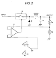
- the electric power converter according to the present embodiment as a voltage drop type switching regulator comprises a switching element 10, comparator 12, free wheel diode D, reactor L, capacitor Cf, resistors Ra and Rb, and switch SW. Switching operation is performed by sequential switching of multiple discrete frequencies f1 to fn by sawtooth wave.
- the switching element 10 consists of a transistor, FET, IGBT and other semiconductors, for example. and the input voltage (d.c. voltage) is switched in response to switching signal.
- the input voltage is converted into the rectangular wave voltage by switching and is output to the side of reactor L.
- the reactor L and capacitor Cf form a low path filter to remove the switching noise contained in the output voltage of switching element 10, thereby allowing only the d.c. component to pass by.
- the reactor L and capacitor Cf are configured to have the function of a filter circuit for smoothing the output voltage of the switching element 10.
- the output voltage of the low path filter is divided by resistors Ra and Rb constituting the voltage divider.
- the divided voltage is input into the negative input terminal of the comparator 12 as a feedback signal.
- Signals selected by switch SW are input to the positive input terminal of the comparator 12.
- the switch SW as a signal selecting means is connected to the signal generator (not illustrated) for generating signals of sawtooth waveform at frequencies f1 to fn. Out of multiple signals, signals having a specified frequency are selected sequentially in the predetermined order, and selected signals are sent to the comparator 12.
- Comparator 12 compares between the feedback signal from the voltage divider and signals selected by switch SW, and PWM (pulse width modulation) control signals in response to the result of comparison are sent to the switching element 10 as switching signals. Then switching operation of switching element 10 is performed by switching signals. In this case, feedback signals of d.c. voltage and signals of sawtooth waveform are compared by the comparator 12, and PWM (pulse width modulation) control signals are changed in response to the result of comparison. For example, when the feedback signal level is increased, the pulse width is reduced. Conversely, when the feedback signal level is decreased, the pulse width is increased. Switching element 10 performs switching operation in response to switching signals with changing pulse width, with the result that the output voltage of the low path filter is controlled to a constant level at all times.
- PWM pulse width modulation
- multiple signals having a different period or frequency are switched in an predetermined order. This allows the peak of the switching noise to be diffused in the frequency range, and noise energy to be diffused, thereby reducing the noise level. Moreover, it ensures a stable reduction of noise level at all times.
- the switching noise is measured when each frequency is selected. This measurement provides a basis for setting a selection pattern in conformity to reduced noise.
- a wave generator for generating signals having a certain tilt for example, a triangular wave generator for producing triangular waves can be used as a signal generator, instead of a signal generator generating a sawtooth waveform.
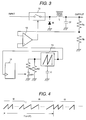
- a circuit structure (a third embodiment) shown in Fig. 3 can be used for implementation of a signal generator for producing signals of sawtooth waveform at frequencies f1 and f2 and a signal selecting means for selecting two signals produced from this signal generator.
- a sawtooth wave generator 14 and a counter (binary counter) 16 are connected as a signal generator and signal selecting means to the positive input end of the comparator 12.
- the signals of sawtooth waveform at two discrete frequencies f1 and f2 are output to the counter 16 and comparator 12 by the sawtooth wave generator 14 as a waveform generator.
- signals having different frequencies and periods are generated from from the sawtooth wave generator 14, so sawtooth wave generator 14 is provided with resistors R0 and R1, switch SW1 and capacitor C.
- Resistor R0 and capacitor C are designed as a time constant circuit to determine the period or frequency of the signals produced from sawtooth wave generator 14 according to the time constant.
- the resistor R1 is provided in parallel through resistor R0 and switch SW1.
- the time constant R is set by the resistors R0 and R1 and switch SW.
- the sawtooth wave frequency is switched according to whether the switch SW21 is opened or closed. For example, the sawtooth wave of the frequency corresponding to time constants C and R0 is selected when the switch SW1 is open. When the switch SW1 is closed, the sawtooth wave of the frequency corresponding to time constants C and 1/(1/R0 + 1/R1) is selected. Signals of sawtooth waveform at frequencies f1 and f2 are produced sequentially by the selection of switch SW1, as illustrated in Fig. 4. In this case, the switch SW1 is opened or closed by the output pulse of the counter 16. The counter 16 counts the signals generated from the sawtooth wave generator 14 and compares this count with the preset value. Then the switch SW1 is selected according to the result of this comparison.
- the counter produces pulses as switching signals synchronously with the vertex of the waveform of the signals generated from the waveform generator 14.
- the output voltage will fluctuate if the switch SW1 is changed in the middle of a sawtooth wave.
- the switch SW1 is designed to open or close at the vertex of the sawtooth wave (i.e. at the maximum or minimum point of the wave), not in the middle of the sawtooth wave. Accordingly, when the sawtooth wave which rises at a certain tilt with the lapse of time is used, the counter 16 operates at the fall of the sawtooth wave. Accordingly, the fluctuation of switching regulator output voltage can be avoided by ensuring the switch SW1 is opened or closed at the vertex of the sawtooth wave.
- the switch SW1 When the triangular wave is used instead of a sawtooth wave, the switch SW1 should be opened or closed at the vertex of the sawtooth wave, namely, at the maximum or minimum point of the wave.
- the triangular wave generator for producing triangular waves is normally implemented by repeating the waveform which has reached the preset threshold value (the upper and lower limit values of the waveform) (namely by switching between electric charging and discharging into the capacitor at a constant current). Capacitor discharging is switched to charging when the voltage has reached the lower limit value of the waveform in the process of capacitor discharging. Capacitor charging is switched to discharging when the voltage has reached the upper limit value of the waveform in the process of capacitor charging.
- the opening/closing operation of the switch SW1 can be carried out at the vertex of the sawtooth wave, if the counter 16 is operated at the time of having reached the threshold value (upper or lower value of the waveform) where the waveform value is preset on the basis of the result of comparison with the threshold value preset on the triangular wave generator.
- capacity value is changed by the opening/closing operation of the switch SW1, and is change the frequency.
- switching of the resistance value by opening/closing operation of the switch is more ecumenical than changing of the capacity value by switching multiple capacitors.
- switching operation is performed by switching the signals of two periods or frequencies in the preset order. This allows the peak of the switching noise to be diffused in the frequency range, and noise energy to be diffused, thereby reducing the noise level. Moreover, it ensures a stable reduction of noise level at all times.
- the inventors of the present invention have made an algebraic calculation to get the frequency spectrum in the present embodiment, and have obtained the switching waveform as shown in Fig. 5. In this case, they try to derive the spectrum when two frequencies f1 and f2 are periodically switched as shown in Fig. 4. In the derivation of this spectrum, they make efforts to obtain the enveloping spectrum in order to generate overlapped waveforms of various signals in the event of alternate generation of signals of frequencies f1 and f2 at period T at a burst, as shown in Figs. 6 (a) and (b).
- the [Eq. 3] can be obtained from [Eq. 1]: Since Fourier transform of ⁇ (t - t o ) is exp (- j2 ⁇ kft o ), Fourier transform of a(t) is given by duality as followed:
- the waveform spectrum of Fig. 4 can be expressed as A1 (f) + A2 (f).
- the switching waveform is as shown in Fig. 5.
- the frequency in Fig. 7 indicates the value obtained by normalizing the measured frequency by means of switching frequency.
- the present embodiment allows the amplitude of the switching noise to be reduced or eliminated by spreading the spectrum of the switching noise generated from the switching regulator and by diffusing the energy of noise, even when a simple circuit configuration shown in Fig. 3 is used.
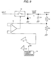
- This embodiment provides the same effect of the first embodiment, and allows the switch SW to be changed in a desired order by the random number generator 18.
- the switch SW is changed by the signals sent from the random number generator 18 in order to select the signals of sawtooth waveform having two discrete frequencies f1 and f2. Otherwise, it is the same as shown in Fig. 2.
- the random number generator 18 is connected to the sawtooth wave generator 14 instead of counter 16, as shown in Fig. 10 (sixth embodiment).
- the switch SW1 is changed by the random number generator 18 actuated synchronously with signals of sawtooth waveform produced from the sawtooth wave generator 14.
- the frequency in Fig. 12 indicates the value obtained by normalizing the measured frequency by means of switching frequency.
- the spectrum is distributed in continuation with the envelope shown in Fig. 5.
- the result of FFT shown in Fig. 12 also gives a spectrum distributed almost in continuation with the envelope shown in Fig. 7.
- the peak value is reduced correspondingly.
- the present embodiment allows the amplitude of the switching noise to be reduced or eliminated by spreading the spectrum of the switching noise generated from the switching regulator and by diffusing the energy of noise, even when a simple circuit configuration shown in Fig. 10 is used.
- the circuit for generating switching signals by sequential selection of the signals of sawtooth waveform having multiple discrete frequencies f1 to fn is implemented in the form of a digital circuit.
- multiple resistors R1, ...., Rn and switches SW1, ..., SWm are connected as binary ladders to the resistor R0 in parallel with the sawtooth wave generator 14.
- the present embodiment is the same as that shown in Fig. 3, except that multiple resistors and switches are provided.
- the sawtooth waves of the frequency corresponding to the time constants C and R ⁇ are generated when switches SW1 to SWm are all open.
- the waveform of the frequency corresponding to C, R0 and time constant determined by the parallel combined resistance of the resistor Ri connected to the closed switch SW1 is generated.
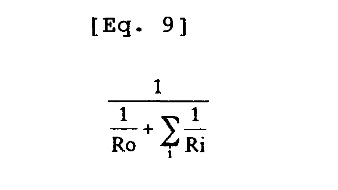
- the parallel combined resistance of the resistor Ri is given by:
- Opening/closing operation of the switch SW1, ..., SWm is controlled by the counter 16 actuated synchronously with sawtooth wave.
- the fluctuation of the switching regulator output voltage is prevented by ensuring that the tilt of sawtooth wave does not change in the middle.
- each resistance Ri is as shown in the following equation: Then "m" resistors provide signals of frequencies corresponding to 2 m parallel combined resistances (a m-th power of 2). In other words, signals of frequencies corresponding to 2 m parallel combined resistances (a m-th power of 2) can be generated if the value of each resistor Ri is set to a value different form the parallel combined resistances when other resistors are connected in parallel.
- Fig. 14 The following describes the eighth embodiment of the present invention with reference to Fig. 14:
- the comparator 12, sawtooth wave generator 14, counter 16 and switches SW1 to SWm are integrated into the LSI (large integrated circuit) 20 using a digital circuit.
- the switches SW1 to SWm having been arranged on the ground side are arranged in the hot side. Otherwise, the configuration is the same as that shown in Fig. 13.
- the switches SW1 to SWm are arranged in the hot side.
- the wiring area is reduced as compared to the case where the switches SW1 to SWm arranged on the ground side are integrated.
- Switches SW1 to SWm can be produced by the transistor (bi-polar or FET).
- Determination of the frequency of the sawtooth wave of the sawtooth wave generator 14 greatly depends on the resistor R0, so the accuracy requirement of resistors R1 to Rm is not so severe as that of the resistor R0. For this reason, switches SW1 to SWm and resistors R1 to Rm can be built in the LSI 20, as shown in Embodiment (ninth embodiment) of Fig. 1. Normally, the resistor built in the LSI exhibits an accuracy up to scores of percent without trimming. This is sufficient for a resistor used merely to change the time constant.
- the signals waveform having multiple discrete frequencies f1 to fn can be produced by increasing the number of resistors and switches.
- the effect diffusing the switching noise of the switching regulator can be improved substantially while the number of parts, price, failure rate and dimensions are reduced.
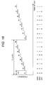
- 3th power of 2 namely, eight frequencies f1 to f8 can be produced by adding three resistors R1, R2 and R3 and switches SW1, SW2 and SW as binary ladders, in addition to resistor R0.
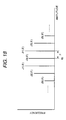
- the target waveform is approximated to the carrier wave of the center frequency fo which is frequency-modulated by the sinusoidal wave of frequency F.
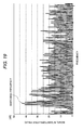
- the frequencies in Fig. 19 and 20 indicate the values obtained by normalizing the measured frequencies by means of switching frequency.
- Fig. 18 reveals that, because of the characteristics of the Bessel function, the bottom portion expands with the increase of ⁇ , and the peak is lowered with the result that the effect of diffusing the switching noise is improved.
- Fig. 20 the spectrum (spectrum with constant frequency) without spectrum diffusion (dither) of switching noise is indicated by a broken line for the sake of comparison. Comparison between the characteristics of this broken line and those of the sequential frequency switching method (solid line) reveals that the noise reduction effect amounts to about 7 dB for the second harmonic wave and about 10 dB for the third and later harmonic waves according to the present invention.
- a circuit configuration in the practical size is used to diffuse the spectrum of the switching noise of the switching regulator and to diffuse the energy of noise, thereby ensuring a stable reduction of the amplitude of switching noise at all times, as discussed above.
- a digital circuit is used to implement the embodiment shown in Fig. 8.
- the random number generator 18 is provided instead of the counter 16 shown in Fig. 13. Otherwise, its configuration is the same as that of Fig. 13. Namely, the opening/closing operation of the switch SW1, ..., SWm is controlled by the random number generator 18 actuating synchronously with sawtooth wave.
- "m" resistors is subjected to random selection by switching signals (pulses) from the random number generator 18. This allows the component of switching noise to be diffused over a still wider range by random selection of 2 m (m-th power of 2) discrete frequency with the result that the peak of switching noise cannot be further reduced.
- the former envelope is uni-modal and the amplitude of the component of the center frequency is the greatest.
- the latter envelope is uni-modal when ⁇ is smaller. If ⁇ is larger, it turns bimodal. Moreover, the peak is low with wider base, and the effect of diffusing the spectrum of the switching noise is increased.
- Fig. 15 provides a substantial reduction of the costs of increasing the number of resistors, with the result that a higher effect can be ensured.
- a much greater effect is ensured by the method for reducing F by increasing the number (n) of discrete frequencies and switching the frequencies alternately in ascending order and descending order.
- the method for switching the frequencies alternately in ascending order and descending order provides a greater effect than random frequency switching even if the random frequency switching method is not used.
- the spectrum diffusion effect is not definite, and greatly depends on the random number sequence in the case of random frequency switching.
- the effect of mass production can be greatly improved if "m" resistors are built in the LSI 20.
- the present invention can be applied to the electric power converter based on switching which has no voltage feedback, in addition to the feedback switching regulator. In this case, it goes without saying that application of this invention reduces the peak of the switching noise of the electric power converter.
- the present embodiment allows a simple circuit configuration to reduce the peak of the switching noise of the d.c. voltage electric power converter which is not required to ensure high voltage stability.
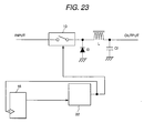
- rectangular waveform generator 22 and counter 16 are provided as a signal generator and signal selecting means as shown in Fig. 23; signals of the rectangular wave at frequencies f1 to fn are output to the switching element 10 from the rectangular waveform generator 22; and the counter 16 is actuated synchronously with this signal. Then switching operation of the switching element 10 can be performed by the signals of rectangular wave at frequencies f1 to fn.
- the rectangular waveform generator 22 When the rectangular waveform generator 22 is implemented, the following two methods can be considered, for example: One is the method of using a frequency divider which divides the original frequency (reference frequency), and the other is the method of using the oscillator circuit where the oscillation frequency is changed according to time constant CR. When the method of frequency divider is used, it is sufficient that the division ratio of the frequency divider constituting the rectangular waveform generator 22 be controlled by the output of the counter 16.
- a free wheel diode D is inserted between the reactor L and capacitor Cf; one end of the switching element 10 is connected to the contact point between the reactor L and free wheel diode D, with the other end of the switching element 10 grounded; and switching operation of the switching element 10 is controlled by the output of the comparator 12.
- a free wheel diode D is inserted between the reactor L and capacitor Cf; the switching element 10 is connected to the contact point between the reactor L and free wheel diode D, with the other end of the switching element 10 grounded; and the rectangular wave from the rectangular waveform generator 22 is applied to the switching element 10.
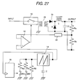
- a transfer 26 is inserted between the switching element 10 and reactor L; the secondary side of the transfer 26 is connected to the re actor L via the diode Dr; an isolator 28 as an insulation amplifier is inserted in the connection point between the resistors Ra and Rb; and the isolator 28 the is connected to the negative input terminal of the comparator 12.
- the present invention can be applied to the insulation type voltage converter circuit as shown in Fig. 28 if use of a feedback system is to be eliminated.
- the present invention can also be applied to the inverter which converts the direct current to the alternating voltage by eliminating the use of a rectifier circuit from the insulation type voltage converter circuit as shown in Fig. 29.
- Fig. 30 shows the embodiment of the electronic device 100 using the switching regulator 101.
- the electronic device 100 comprises the switching regulator 101 and electronic circuit 102 as the load of the switching regulator 101.
- the switching regulator 101 is designed to convert 12-volt (14-volt) or 42-volt d.c. voltage into 5-, 3.3-, 3.5- and 1.8-volt d.c. voltages, and is output.
- the electronic circuit 102 for example, as a controlling means for controlling the car engine, automatic speed changer and brake,is designed to be operated by 5-, 3.3-, 2.5- and 1.8-volt d. c. voltages input from the switching regulator 101.
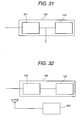
- the level of the switching noise produced from the switching regulator 101 is very small when the output of the switching regulator 101 is led to the outside as power supply for an element different from the electronic circuit 102, for example, a sensor as shown in Fig. 31. This makes it possible to prevent switching noise from leaking out via the power supply line.
- comparator 12 counter 16 and sawtooth wave generator 14 are made up of digital circuits can be produced in a smaller space.
- Their circuit configuration is especially suited for formation of an integrated circuit.
- the present invention allows the peak of the switching noise to be diffused in the frequency range, and noise energy to be diffused, thereby ensuring a stable reduction of noise level at all times.
Landscapes
- Engineering & Computer Science (AREA)
- Power Engineering (AREA)
- Dc-Dc Converters (AREA)
Abstract
Description
a signal generator for generating multiple signals having different frequencies,
a signal selecting means for selecting signals of specified frequency
from said multiple signals and outputting said signals sequentially in the predetermined order,
a switching element for switching input voltage in response to signals selected by said signal selecting means, and
a filter circuit for smoothing the output voltage of said switching element.
a switching element for switching input voltage in response to switching signals,
a filter circuit for smoothing the output voltage of said switching element,
a signal generator for generating multiple signals having different frequencies,
a signal selecting means for selecting signals of specified frequency from said multiple signals and outputting said signals sequentially in the predetermined order, and
a comparator which compares between signals selected by said signal selecting means and feedback signals obtained from the output voltage of said filter circuit, thereby generating switching signals and outputting them to said switching element.
a waveform generator for generating signals of triangular waveform and sawtooth wave,
a time constant circuit for determining the period of the signals generated from the waveform generator according time constant,
multiple resistors for changing the time constant,
a counter which counts the signals generated from the waveform generator, compares the counted value with the preset value and outputs the switching signals synchronously with the vertex of the waveform of the signals based on the compared result, and
multiple switch for adding the specified ones of the multiple resistors to the time constant circuit in response to the switching signals.
a waveform generator for generating signals of triangular waveform and sawtooth waveform,
a time constant circuit for determining the period of the signals generated from the waveform generator according time constant,
multiple resistors for changing the time constant,
a random number generator for outputting the switching signals synchronously with the vertex of the waveform of the signals generated from the waveform generator, and
multiple switch for adding the specified ones of the multiple resistors to the time constant circuit in response to the switching signals.


Thus, the [Eq. 3] can be obtained from [Eq. 1]:


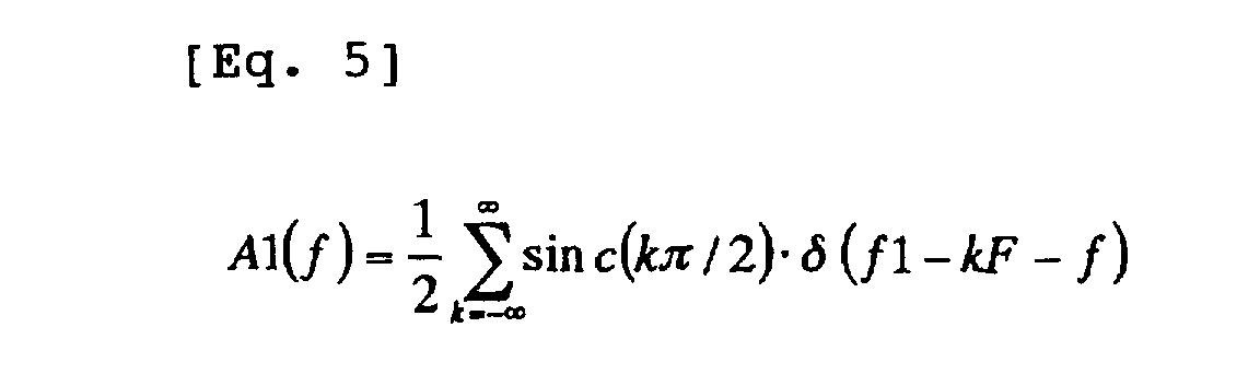


This is expanded into an infinite series, as shown in the following equation.


The
Claims (26)
- An electric power converter comprising:a signal generator for generating multiple signals having different frequencies,a signal selecting means for selecting signals of specified frequency from said multiple signals and outputting said signals sequentially in the predetermined order,a switching element (10) for switching input voltage in response to signals selected by said signal selecting means, anda filter circuit for smoothing the output voltage of said switching element (10).
- An electric power converter according to Claim 1, wherein multiple signals generated from said signal generator (14) are signals of rectangular waves having different periods.
- An electric power converter comprising:a switching element (10) for switching input voltage in response to switching signals,a filter circuit for smoothing the output voltage of said switching element (10),a signal generator for generating multiple signals having different frequencies,a signal selecting means for selecting signals of specified frequency from said multiple signals and outputting said signals sequentially in the predetermined order, anda comparator (12) which compares between signals selected by said signal selecting means and feedback signals obtained from the output voltage of said filter circuit, thereby generating switching signals and outputting them to said switching element (10).
- An electric power converter according to Claim 3, wherein multiple signals generated from said signal generator are the signals characterized by waveforms having a certain tilt.
- An electric power converter according to Claim 3, wherein multiple signals generated from said signal generator are the signals characterized by sawtooth waveforms.
- An electric power converter according to Claim 3, wherein multiple signals generated from said signal generator are the signals characterized by triangular waveforms.
- An electric power converter according to any one of Claims 4, 5 and 6, wherein said signal selecting means selects the signals generated from said signal generator according to the vertex of the waveform.
- An electric power converter according to any one of Claims 1 through 7, wherein said signal selecting means repeats the step of selecting out of the signals generated from said signal generator the signals in the order from lower to higher frequencies, and then selecting said signals in the order from higher to lower frequencies.
- An electric power converter according to Claim 3, wherein said signal generator and said signal selecting means comprise:a waveform generator (14) for generating signals of triangular waveform or sawtooth waveform,a time constant circuit for determining the period of the signals generated from said waveform generator (14) according to a time constant,multiple resistors for changing said time constant,a counter (16) which counts the signals generated from said waveform generator (14), compares the counted value with the preset value and outputs the switching signals synchronously with the vertex of the waveform of said signals based on the compared result, andmultiple switches for adding the specified ones of said multiple resistors to said time constant circuit in response to said switching signals.
- An electric power converter according to Claim 3, wherein said signal generator and said signal selecting means comprise:a waveform generator (14) for generating signals of triangular waveform or sawtooth waveform,a time constant circuit for determining the period of the signals generated from said waveform generator (14) according to a time constant,multiple resistors for changing said time constant,a random number generator (18) for outputting the switching signals synchronously with the vertex of the waveform of the signals generated from said waveform generator (14), andmultiple switches for adding the specified ones of said multiple resistors to said time constant circuit in response to said switching signals.
- An electric power converter according to Claim 9, wherein said counter (16) is a binary counter.
- An electric power converter according to Claim 9 or 11, wherein said waveform generator (14), said comparator (12), said multiple switches and said counter (16) are arranged on a single semiconductor chip.
- An electric power converter according to Claim 9 or 11, wherein said waveform generator (14), said comparator (12), said multiple resistors, said multiple switches and said counter (16) are arranged on a single semiconductor chip.
- An electric power converter according to Claim 10, wherein said waveform generator (14), said comparator (12), said multiple switches and said random number generator (18) are arranged on a single semiconductor chip.
- An electric power converter according to Claim 10, wherein said waveform generator (14), said comparator (12), said multiple resistors, said multiple switches and said random number generator (18) are arranged on a single semiconductor chip.
- An electric power converter according to any one of Claims 9, 10, 11, 12, 13, 14 and 15, wherein said multiple resistors and said multiple switches are each connected in series, and resistors and switches connected in series are each connected with others in parallel.
- An electric power converter according to Claim 16, wherein the resistance of each of said resistors is different from the parallel combined resistance of other resistors connected in parallel.
- An electric power converter according to Claim 17, wherein the resistance Ri of each of said resistors has a relation of Ri = Kr.2-1.
- An electric power converter according to Claim 2, wherein said signal generator consists of a frequency divider for dividing the original frequency.
- An electric power converter according to any one of Claims 1 through 19, wherein a transformer (26) is provided between said switching element (10) and said filter circuit.
- An electric power converter according to any one of Claims 1 through 19, wherein said filter circuit has a reactor and capacitor, one end of said reactor is connected to the input side, and the other end of said reactor is connected to the ground via said capacitor as well as via said switching element.
- An electronic apparatus wherein an electric power converter according to any one of Claims 1 through 21, characterized by an electronic circuit to be operated by power received from said electric power converter.
- An electronic apparatus according to Claim 22, wherein the output of said electric power converter is led outside as a power source for the element different from said electronic circuit.
- An electronic apparatus according to Claim 22, wherein the output of said electric power converter is arranged in the vicinity of a receiving apparatus.
- An electronic apparatus according to Claim 22, wherein said electronic circuit has a control means for controlling any one of a car engine, automatic changer and brake.
- A car comprising an electronic apparatus according to Claim 25.
Applications Claiming Priority (2)
| Application Number | Priority Date | Filing Date | Title |
|---|---|---|---|
| JP2001049801A JP3718830B2 (en) | 2001-02-26 | 2001-02-26 | Power converter |
| JP2001049801 | 2001-02-26 |
Publications (2)
| Publication Number | Publication Date |
|---|---|
| EP1235335A2 true EP1235335A2 (en) | 2002-08-28 |
| EP1235335A3 EP1235335A3 (en) | 2003-08-27 |
Family
ID=18910856
Family Applications (1)
| Application Number | Title | Priority Date | Filing Date |
|---|---|---|---|
| EP01119693A Withdrawn EP1235335A3 (en) | 2001-02-26 | 2001-08-23 | Electric power converter |
Country Status (3)
| Country | Link |
|---|---|
| US (1) | US6600295B2 (en) |
| EP (1) | EP1235335A3 (en) |
| JP (1) | JP3718830B2 (en) |
Cited By (4)
| Publication number | Priority date | Publication date | Assignee | Title |
|---|---|---|---|---|
| WO2004084392A2 (en) | 2003-03-17 | 2004-09-30 | Rf Micro Devices, Inc. | Dc-dc converter with reduced electromagnetic interference |
| US7413413B2 (en) | 2004-07-20 | 2008-08-19 | York International Corporation | System and method to reduce acoustic noise in screw compressors |
| EP2393191A3 (en) * | 2010-05-07 | 2013-03-06 | Silicon Works Co., Ltd. | Boost converter for liquid crystal display |
| CN112398334A (en) * | 2019-08-14 | 2021-02-23 | 飞虹高科股份有限公司 | Voltage-reducing integrated circuit |
Families Citing this family (40)
| Publication number | Priority date | Publication date | Assignee | Title |
|---|---|---|---|---|
| JP2799446B2 (en) * | 1993-07-22 | 1998-09-17 | 矢崎総業株式会社 | connector |
| JP3963257B2 (en) * | 2002-02-14 | 2007-08-22 | 富士通株式会社 | DC-DC converter, electronic equipment, duty ratio setting circuit |
| US6977492B2 (en) * | 2002-07-10 | 2005-12-20 | Marvell World Trade Ltd. | Output regulator |
| US6833693B2 (en) * | 2003-04-30 | 2004-12-21 | Agilent Technologies, Inc. | EMI reduction of power converters by way of controlled randomized modulation of oscillating signals |
| US7218531B2 (en) * | 2004-04-05 | 2007-05-15 | Elster Electricity, Llc | Switching regulator with reduced conducted emissions |
| US7362191B2 (en) * | 2004-04-29 | 2008-04-22 | Linear Technology Corporation | Methods and circuits for frequency modulation that reduce the spectral noise of switching regulators |
| DE102004021344A1 (en) * | 2004-04-30 | 2005-11-17 | Micronas Gmbh | DC converter |
| JP4681830B2 (en) * | 2004-06-24 | 2011-05-11 | パナソニック株式会社 | PWM circuit and PWM circuit control method |
| JP4622423B2 (en) * | 2004-09-29 | 2011-02-02 | 日本テキサス・インスツルメンツ株式会社 | Pulse width modulation signal generation circuit |
| JP2006109039A (en) * | 2004-10-05 | 2006-04-20 | Mitsubishi Electric Corp | Class D amplifier |
| JP4467581B2 (en) | 2004-10-29 | 2010-05-26 | ローム株式会社 | Switching regulator control circuit, switching regulator using the same, and electronic equipment |
| JP4198677B2 (en) * | 2004-12-28 | 2008-12-17 | 株式会社デンソー | Power switching equipment |
| DE602005008475D1 (en) * | 2004-12-30 | 2008-09-04 | Koninkl Philips Electronics Nv | MONITORING THE TEMPERATURE DEPENDENCE OF THE EXTERNAL CAPACITORS OF A CHARGE PUMP AND IMPROVED CHARGING PUMPS THEREOF |
| JP4630165B2 (en) * | 2005-09-21 | 2011-02-09 | パナソニック株式会社 | DC-DC converter |
| JP4976797B2 (en) * | 2005-09-29 | 2012-07-18 | クラリオン株式会社 | Switching power supply |
| JP4816508B2 (en) * | 2007-03-02 | 2011-11-16 | ヤマハ株式会社 | ΔΣ AD converter, class D amplifier, and DC-DC converter |
| JP2008283798A (en) | 2007-05-11 | 2008-11-20 | Matsushita Electric Ind Co Ltd | Switching control device |
| FI20075645A0 (en) * | 2007-09-17 | 2007-09-17 | Nokia Corp | Control circuit and dittering method |
| US7728571B2 (en) * | 2007-11-06 | 2010-06-01 | Richtek Technology Corporation, R.O.C. | Load-dependent frequency jittering circuit and load-dependent frequency jittering method |
| JP5239360B2 (en) | 2008-01-31 | 2013-07-17 | 株式会社リコー | Switching power supply circuit |
| US9298303B2 (en) * | 2009-12-31 | 2016-03-29 | Google Technology Holdings LLC | Duty cycle modulation of periodic time-synchronous receivers for noise reduction |
| JP5625369B2 (en) | 2010-01-28 | 2014-11-19 | ミツミ電機株式会社 | Buck-boost DC-DC converter and switching control circuit |
| JP5493916B2 (en) * | 2010-01-28 | 2014-05-14 | ミツミ電機株式会社 | Buck-boost DC-DC converter and switching control circuit |
| US9203489B2 (en) | 2010-05-05 | 2015-12-01 | Google Technology Holdings LLC | Method and precoder information feedback in multi-antenna wireless communication systems |
| JP2011254665A (en) * | 2010-06-03 | 2011-12-15 | On Semiconductor Trading Ltd | Control circuit of light-emitting element |
| CN102158085B (en) * | 2011-03-11 | 2013-05-01 | 复旦大学 | Digital automatic frequency-selecting direct current converter |
| US9813262B2 (en) | 2012-12-03 | 2017-11-07 | Google Technology Holdings LLC | Method and apparatus for selectively transmitting data using spatial diversity |
| US9591508B2 (en) | 2012-12-20 | 2017-03-07 | Google Technology Holdings LLC | Methods and apparatus for transmitting data between different peer-to-peer communication groups |
| US9979531B2 (en) | 2013-01-03 | 2018-05-22 | Google Technology Holdings LLC | Method and apparatus for tuning a communication device for multi band operation |
| JP5645979B2 (en) * | 2013-01-25 | 2014-12-24 | 三菱電機株式会社 | DIGITAL CONTROL POWER SUPPLY DEVICE AND DIGITAL CONTROL OPERATION METHOD |
| US10229697B2 (en) | 2013-03-12 | 2019-03-12 | Google Technology Holdings LLC | Apparatus and method for beamforming to obtain voice and noise signals |
| WO2014192373A1 (en) * | 2013-05-27 | 2014-12-04 | 株式会社東芝 | Power conversion device, power conversion device control method, rotation sensorless control device, and rotation sensorless control device control method |
| JP6261889B2 (en) * | 2013-06-24 | 2018-01-17 | 株式会社東芝 | Rotation sensorless control device, control method and control program for rotation sensorless control device |
| US9386542B2 (en) | 2013-09-19 | 2016-07-05 | Google Technology Holdings, LLC | Method and apparatus for estimating transmit power of a wireless device |
| US9549290B2 (en) | 2013-12-19 | 2017-01-17 | Google Technology Holdings LLC | Method and apparatus for determining direction information for a wireless device |
| US9491007B2 (en) | 2014-04-28 | 2016-11-08 | Google Technology Holdings LLC | Apparatus and method for antenna matching |
| US9478847B2 (en) | 2014-06-02 | 2016-10-25 | Google Technology Holdings LLC | Antenna system and method of assembly for a wearable electronic device |
| DE102017001788A1 (en) * | 2017-02-24 | 2018-08-30 | Leopold Kostal Gmbh & Co. Kg | Method for controlling an electrical consumer by means of pulse width modulation |
| CN111756219A (en) * | 2020-07-05 | 2020-10-09 | 上海韦孜美电子科技有限公司 | A switching frequency jittering method, switching circuit and DC-DC converter |
| US12193662B2 (en) * | 2020-07-16 | 2025-01-14 | Cilag Gmbh International | Firing circuit and control algorithm for surgical stapler |
Family Cites Families (20)
| Publication number | Priority date | Publication date | Assignee | Title |
|---|---|---|---|---|
| US3777277A (en) * | 1973-02-23 | 1973-12-04 | Us Navy | Discrete step frequency sweep |
| JPS53101622A (en) * | 1977-02-16 | 1978-09-05 | Meidensha Electric Mfg Co Ltd | Controller for pwm inverter |
| US4190882A (en) * | 1977-05-05 | 1980-02-26 | Hughes Aircraft Company | System for reducing the effects of power supply switching |
| US4188585A (en) * | 1978-03-16 | 1980-02-12 | Cincinnati Electronics Corporation | Synchronized receiver power system |
| US4638417A (en) * | 1985-08-16 | 1987-01-20 | Sperry Corporation | Power density spectrum controller |
| DE3539558A1 (en) * | 1985-11-07 | 1987-05-21 | Siemens Ag | METHOD AND CIRCUIT FOR GENERATING A CLOCK FREQUENCY FOR POWER ELECTRONIC DEVICES AND MACHINES |
| GB8907918D0 (en) * | 1989-04-07 | 1989-05-24 | Chloride Group Plc | Improvements in controllers for electrical loads |
| JP2989234B2 (en) * | 1990-08-14 | 1999-12-13 | 沖電気工業株式会社 | CR oscillator and transmission frequency adjusting method thereof |
| US5416481A (en) | 1993-09-24 | 1995-05-16 | Advanced Micro Devices, Inc. | Analog-to-digital converter with multi-level dither current input |
| US5640315A (en) | 1994-03-18 | 1997-06-17 | Nippon Steel Corporation | Switching regulator |
| JPH07264849A (en) | 1994-03-18 | 1995-10-13 | Nippon Steel Corp | Switching regulator |
| EP0681362B1 (en) * | 1994-05-06 | 1998-10-28 | STMicroelectronics S.r.l. | Digital current mode PWM control |
| US5907482A (en) * | 1995-11-30 | 1999-05-25 | Toko, Inc. | Power supply control device |
| US5757338A (en) * | 1996-08-21 | 1998-05-26 | Neomagic Corp. | EMI reduction for a flat-panel display controller using horizontal-line based spread spectrum |
| US5982156A (en) * | 1997-04-15 | 1999-11-09 | The United States Of America As Represented By The Secretary Of The Air Force | Feed-forward control of aircraft bus dc boost converter |
| US6049471A (en) * | 1998-02-11 | 2000-04-11 | Powerdsine Ltd. | Controller for pulse width modulation circuit using AC sine wave from DC input signal |
| KR100286047B1 (en) * | 1998-05-15 | 2001-04-16 | 김덕중 | Power Factor Correction Circuit Using Inverse Sawtooth Wave |
| JP2000217340A (en) * | 1999-01-21 | 2000-08-04 | Fujitsu Ltd | Method of generating rectangular wave signal with maximum duty ratio, duty ratio setting circuit, and DC-DC converter |
| US6018467A (en) * | 1999-07-28 | 2000-01-25 | Philips Electronics North America Corporation | Resonant mode power supply having an efficient low power stand-by mode |
| US6166527A (en) * | 2000-03-27 | 2000-12-26 | Linear Technology Corporation | Control circuit and method for maintaining high efficiency in a buck-boost switching regulator |
-
2001
- 2001-02-26 JP JP2001049801A patent/JP3718830B2/en not_active Expired - Fee Related
- 2001-08-23 EP EP01119693A patent/EP1235335A3/en not_active Withdrawn
- 2001-08-31 US US09/943,386 patent/US6600295B2/en not_active Expired - Fee Related
Cited By (6)
| Publication number | Priority date | Publication date | Assignee | Title |
|---|---|---|---|---|
| WO2004084392A2 (en) | 2003-03-17 | 2004-09-30 | Rf Micro Devices, Inc. | Dc-dc converter with reduced electromagnetic interference |
| WO2004084392A3 (en) * | 2003-03-17 | 2004-12-09 | Rf Micro Devices Inc | Dc-dc converter with reduced electromagnetic interference |
| US6969978B2 (en) | 2003-03-17 | 2005-11-29 | Rf Micro Devices, Inc. | DC-DC converter with reduced electromagnetic interference |
| US7413413B2 (en) | 2004-07-20 | 2008-08-19 | York International Corporation | System and method to reduce acoustic noise in screw compressors |
| EP2393191A3 (en) * | 2010-05-07 | 2013-03-06 | Silicon Works Co., Ltd. | Boost converter for liquid crystal display |
| CN112398334A (en) * | 2019-08-14 | 2021-02-23 | 飞虹高科股份有限公司 | Voltage-reducing integrated circuit |
Also Published As
| Publication number | Publication date |
|---|---|
| US20020149351A1 (en) | 2002-10-17 |
| JP3718830B2 (en) | 2005-11-24 |
| US6600295B2 (en) | 2003-07-29 |
| JP2002252970A (en) | 2002-09-06 |
| EP1235335A3 (en) | 2003-08-27 |
Similar Documents
| Publication | Publication Date | Title |
|---|---|---|
| US6600295B2 (en) | Electric power converter with continuous stable noise reduction | |
| US7362191B2 (en) | Methods and circuits for frequency modulation that reduce the spectral noise of switching regulators | |
| US7595623B2 (en) | Methods and apparatus for a spread spectrum switching regulator | |
| US7684462B2 (en) | System and method for controlling variations of switching frequency | |
| US10069408B2 (en) | Switched capacitor circuit modifying voltage on the inductor of a buck regulator | |
| US12051973B2 (en) | Multiple dithering profile signal generation | |
| US20160191029A1 (en) | Spread-spectrum clock generation circuit, integrated circuit and apparatus therefor | |
| US20120126768A1 (en) | Control circuit for switching power supply | |
| EP1465329A2 (en) | Multi-output DC-DC converter | |
| EP3206301B1 (en) | Oscillation circuit | |
| WO2011091261A2 (en) | Method and apparatus for frequency-modulation control of an oscillator | |
| US7912112B2 (en) | Spectrum spreading circuit | |
| US11677315B2 (en) | Load adaptive spread spectrum modulation (SSM) | |
| KR101009333B1 (en) | High pressure calibration waveform generator for evaluating response characteristics of DC high voltage power generator and impulse measuring instrument. | |
| US20230327556A1 (en) | Direct current power supply apparatus | |
| Subotskaya et al. | Emission reduction with spread spectrum clocking for switched capacitor buck converter | |
| KR20050121198A (en) | Pulse generator | |
| KR102197788B1 (en) | Dc-dc converter based on chaotic modulation | |
| US12573937B2 (en) | Method and system for modifying carrier signals during phase-shifted pulse width modulation | |
| Kobori et al. | Band Selective Notch Frequency Technology of EMI Noise Spectrum in DC-DC Switching Converters | |
| WO2023286459A1 (en) | Signal generation circuit, switching device, and switching power supply device | |
| JPH0923640A (en) | Pulse width modulation circuit for dc/dc converter | |
| TW200826449A (en) | DC-DC converter and related control apparatus and signal generating method |
Legal Events
| Date | Code | Title | Description |
|---|---|---|---|
| PUAI | Public reference made under article 153(3) epc to a published international application that has entered the european phase |
Free format text: ORIGINAL CODE: 0009012 |
|
| AK | Designated contracting states |
Kind code of ref document: A2 Designated state(s): AT BE CH CY DE DK ES FI FR GB GR IE IT LI LU MC NL PT SE TR |
|
| AX | Request for extension of the european patent |
Free format text: AL;LT;LV;MK;RO;SI |
|
| RIC1 | Information provided on ipc code assigned before grant |
Ipc: 7H 02M 1/12 B Ipc: 7H 02M 3/156 A |
|
| PUAL | Search report despatched |
Free format text: ORIGINAL CODE: 0009013 |
|
| AK | Designated contracting states |
Designated state(s): AT BE CH CY DE DK ES FI FR GB GR IE IT LI LU MC NL PT SE TR |
|
| AX | Request for extension of the european patent |
Extension state: AL LT LV MK RO SI |
|
| RIC1 | Information provided on ipc code assigned before grant |
Ipc: 7H 03B 23/00 B Ipc: 7H 02M 1/12 B Ipc: 7H 02M 3/156 A |
|
| 17P | Request for examination filed |
Effective date: 20031210 |
|
| AKX | Designation fees paid |
Designated state(s): DE FR GB IT |
|
| STAA | Information on the status of an ep patent application or granted ep patent |
Free format text: STATUS: THE APPLICATION HAS BEEN WITHDRAWN |
|
| 18W | Application withdrawn |
Effective date: 20091028 |