EP1235282A2 - Method for fabricating a nitride film - Google Patents
Method for fabricating a nitride film Download PDFInfo
- Publication number
- EP1235282A2 EP1235282A2 EP02004107A EP02004107A EP1235282A2 EP 1235282 A2 EP1235282 A2 EP 1235282A2 EP 02004107 A EP02004107 A EP 02004107A EP 02004107 A EP02004107 A EP 02004107A EP 1235282 A2 EP1235282 A2 EP 1235282A2
- Authority
- EP
- European Patent Office
- Prior art keywords
- nitride film
- iii nitride
- lower region
- upper region
- fabricating method
- Prior art date
- Legal status (The legal status is an assumption and is not a legal conclusion. Google has not performed a legal analysis and makes no representation as to the accuracy of the status listed.)
- Granted
Links
Images
Classifications
-
- C—CHEMISTRY; METALLURGY
- C30—CRYSTAL GROWTH
- C30B—SINGLE-CRYSTAL GROWTH; UNIDIRECTIONAL SOLIDIFICATION OF EUTECTIC MATERIAL OR UNIDIRECTIONAL DEMIXING OF EUTECTOID MATERIAL; REFINING BY ZONE-MELTING OF MATERIAL; PRODUCTION OF A HOMOGENEOUS POLYCRYSTALLINE MATERIAL WITH DEFINED STRUCTURE; SINGLE CRYSTALS OR HOMOGENEOUS POLYCRYSTALLINE MATERIAL WITH DEFINED STRUCTURE; AFTER-TREATMENT OF SINGLE CRYSTALS OR A HOMOGENEOUS POLYCRYSTALLINE MATERIAL WITH DEFINED STRUCTURE; APPARATUS THEREFOR
- C30B25/00—Single-crystal growth by chemical reaction of reactive gases, e.g. chemical vapour-deposition growth
- C30B25/02—Epitaxial-layer growth
-
- C—CHEMISTRY; METALLURGY
- C30—CRYSTAL GROWTH
- C30B—SINGLE-CRYSTAL GROWTH; UNIDIRECTIONAL SOLIDIFICATION OF EUTECTIC MATERIAL OR UNIDIRECTIONAL DEMIXING OF EUTECTOID MATERIAL; REFINING BY ZONE-MELTING OF MATERIAL; PRODUCTION OF A HOMOGENEOUS POLYCRYSTALLINE MATERIAL WITH DEFINED STRUCTURE; SINGLE CRYSTALS OR HOMOGENEOUS POLYCRYSTALLINE MATERIAL WITH DEFINED STRUCTURE; AFTER-TREATMENT OF SINGLE CRYSTALS OR A HOMOGENEOUS POLYCRYSTALLINE MATERIAL WITH DEFINED STRUCTURE; APPARATUS THEREFOR
- C30B29/00—Single crystals or homogeneous polycrystalline material with defined structure characterised by the material or by their shape
- C30B29/10—Inorganic compounds or compositions
- C30B29/40—AIIIBV compounds wherein A is B, Al, Ga, In or Tl and B is N, P, As, Sb or Bi
- C30B29/403—AIII-nitrides
-
- H—ELECTRICITY
- H10—SEMICONDUCTOR DEVICES; ELECTRIC SOLID-STATE DEVICES NOT OTHERWISE PROVIDED FOR
- H10P—GENERIC PROCESSES OR APPARATUS FOR THE MANUFACTURE OR TREATMENT OF DEVICES COVERED BY CLASS H10
- H10P14/00—Formation of materials, e.g. in the shape of layers or pillars
- H10P14/20—Formation of materials, e.g. in the shape of layers or pillars of semiconductor materials
- H10P14/24—Formation of materials, e.g. in the shape of layers or pillars of semiconductor materials using chemical vapour deposition [CVD]
-
- H—ELECTRICITY
- H10—SEMICONDUCTOR DEVICES; ELECTRIC SOLID-STATE DEVICES NOT OTHERWISE PROVIDED FOR
- H10P—GENERIC PROCESSES OR APPARATUS FOR THE MANUFACTURE OR TREATMENT OF DEVICES COVERED BY CLASS H10
- H10P14/00—Formation of materials, e.g. in the shape of layers or pillars
- H10P14/20—Formation of materials, e.g. in the shape of layers or pillars of semiconductor materials
- H10P14/29—Formation of materials, e.g. in the shape of layers or pillars of semiconductor materials characterised by the substrates
- H10P14/2901—Materials
- H10P14/2921—Materials being crystalline insulating materials
-
- H—ELECTRICITY
- H10—SEMICONDUCTOR DEVICES; ELECTRIC SOLID-STATE DEVICES NOT OTHERWISE PROVIDED FOR
- H10P—GENERIC PROCESSES OR APPARATUS FOR THE MANUFACTURE OR TREATMENT OF DEVICES COVERED BY CLASS H10
- H10P14/00—Formation of materials, e.g. in the shape of layers or pillars
- H10P14/20—Formation of materials, e.g. in the shape of layers or pillars of semiconductor materials
- H10P14/32—Formation of materials, e.g. in the shape of layers or pillars of semiconductor materials characterised by intermediate layers between substrates and deposited layers
- H10P14/3202—Materials thereof
- H10P14/3214—Materials thereof being Group IIIA-VA semiconductors
- H10P14/3216—Nitrides
-
- H—ELECTRICITY
- H10—SEMICONDUCTOR DEVICES; ELECTRIC SOLID-STATE DEVICES NOT OTHERWISE PROVIDED FOR
- H10P—GENERIC PROCESSES OR APPARATUS FOR THE MANUFACTURE OR TREATMENT OF DEVICES COVERED BY CLASS H10
- H10P14/00—Formation of materials, e.g. in the shape of layers or pillars
- H10P14/20—Formation of materials, e.g. in the shape of layers or pillars of semiconductor materials
- H10P14/34—Deposited materials, e.g. layers
- H10P14/3402—Deposited materials, e.g. layers characterised by the chemical composition
- H10P14/3414—Deposited materials, e.g. layers characterised by the chemical composition being group IIIA-VIA materials
- H10P14/3416—Nitrides
-
- H—ELECTRICITY
- H10—SEMICONDUCTOR DEVICES; ELECTRIC SOLID-STATE DEVICES NOT OTHERWISE PROVIDED FOR
- H10H—INORGANIC LIGHT-EMITTING SEMICONDUCTOR DEVICES HAVING POTENTIAL BARRIERS
- H10H20/00—Individual inorganic light-emitting semiconductor devices having potential barriers, e.g. light-emitting diodes [LED]
- H10H20/01—Manufacture or treatment
- H10H20/011—Manufacture or treatment of bodies, e.g. forming semiconductor layers
- H10H20/013—Manufacture or treatment of bodies, e.g. forming semiconductor layers having light-emitting regions comprising only Group III-V materials
- H10H20/0133—Manufacture or treatment of bodies, e.g. forming semiconductor layers having light-emitting regions comprising only Group III-V materials with a substrate not being Group III-V materials
- H10H20/01335—Manufacture or treatment of bodies, e.g. forming semiconductor layers having light-emitting regions comprising only Group III-V materials with a substrate not being Group III-V materials the light-emitting regions comprising nitride materials
Definitions
- This invention relates to a method for fabricating a nitride film, particularly a III nitride film usable as an underfilm of a semiconductor element such as a light-emitting diode or a high velocity IC chip.
- III nitride films are employed as semiconductor films for photonic devices constituting a light-emitting diode, etc., and recently, win a lot of attention as semiconductor films for electronic devices, for example, constituting high velocity IC chips to be used in cellular phones.
- III nitride films are usually fabricated by MOCVD methods. Concretely, a substrate on which III nitride films are formed is set onto a susceptor installed in a given reactor, and then, heated to 1000°C or over with a heater provided in or out of the susceptor. Thereafter, raw material gases are introduced with a carrier gas into the reactor and supplied onto the substrate.
- the raw material gases are dissolved through thermochemical reaction into constituent elements, which are reacted to deposit and fabricate a desired III nitride film on the substrate.
- the lattice constant of the III nitride film is affected largely by the composition of the film itself. Therefore, if the composition of the III nitride film is selected, the difference in lattice constant between the substrate and the III nitride film may become large, so that many misfit dislocations may be created at the boundary between the substrate and the III nitride film.
- this invention relates to a method for fabricating a III nitride film, comprising the steps of:
- the inventors had intensely studied to obtain a III nitride film with lower dislocation density through an easy fabricating process without a patterned mask made of SiO 2 . As a result, they found out that by forming the above-mentioned boundary face in the III nitride film, the dislocation density of the III nitride film can be reduced, and thus, the crystal quality of the III nitride film can be improved.
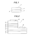
- Fig. 1 is an explanatory view of a fabricating method of a III nitride film according to the present invention.
- a III nitride film 1 including Al element shown in Fig. 1 a boundary face 2 is formed and thus, the III nitride film is divided into two regions 3 and 4.
- the Al content of the upper region 4 is lower than the Al content of the lower region 3 by 10 atomic percentages or over.
- the Al content of the lower region 3 is set to 50 atomic percentages or over.
- the Al content as mentioned above is defined as the amount included in all of the III elements in the III nitride film.
- the III nitride film 1 is fabricated on a given substrate (not shown), and thus, the much dislocations may be created, originated from the dislocations contained in the substrate and the misfit dislocations between the substrate and the III nitride film 1 due to the large difference in lattice constant.
- the dislocation propagation in the III nitride film can be inhibited by the boundary face 2. Therefore, if many dislocations are propagated in the III nitride film 1, they can not be propagated beyond the boundary face 2, and thus, remain only in the lower region 3 or at the boundary face 2. As a result, the dislocation density of the III nitride film can be reduced in the upper region 4.
- the crystal quality of the upper region 4 of the III nitride film 1 can be improved. Therefore, if a given function is provided in the upper region 4 in advance, the III nitride film 1 can be employed as a given semiconductor film entirely.
- the III nitride film 1 is preferably used as an underfilm of a semiconductor element such as a semiconductor light-emitting element, e.g., a light-emitting diode or a high velocity IC chip.
- a semiconductor element such as a semiconductor light-emitting element, e.g., a light-emitting diode or a high velocity IC chip.
- the crystal quality of the semiconductor layer can be improved.
- the luminous efficiency or the high velocity response of the semiconductor element can be remarkably enhanced.
- III nitride film of the present invention a boundary face is formed in a III nitride film to be divided in two region in the thickness direction.
- the screw-type dislocations and the mixed dislocations in the lower region of the III nitride film disappear effectively, and thus, the dislocation density of the upper region of the III nitride film can be also improved more effectively.
- the crystallinity of the lower region of the III nitride film can be also improved entirely up to 90 seconds or below in full width of half maximum (FWHM) of X-ray rocking curve at (002) reflection, and thus, the crystallinity of the upper region can be also enhanced, compared with a conventional III nitride film fabricated by using a buffer layer fabricated at lower temperature.
- FWHM full width of half maximum
- the upper limited value of the fabrication temperature of the lower region of the III nitride film is not restricted, but is preferably set 1250°C. If the upper limited value is set at a temperature beyond 1250°C, the dislocation can not vanish more, and particularly, the crystal quality of the upper region of the III nitride film may be deteriorated due to the surface roughness.
- the III nitride film is made, preferably at 1100°C or over, by a MOCVD method using an Al raw material gas, a nitrogen raw material gas and another raw material gas such as a Ga raw material gas.
- a MOCVD method using an Al raw material gas, a nitrogen raw material gas and another raw material gas such as a Ga raw material gas.
- the amount of supplied Al raw material gas is set larger, and in forming the upper region, the amount of the supplied Al raw material gas is set smaller, so that the Al content in the upper region is set smaller than the Al content in the lower region by 10 atomic percentages or over.
- the boundary face which divides the III nitride film into the lower region and the upper region stepwisely by the difference in Al content of 10 atomic percentage or over, is formed inevitably.
- the dislocation propagation can be inhibited by the boundary face, and thus, the dislocation density in the upper region can be reduced one-fifth as much as that in the lower region, and concretely can be reduced up to 10 8 -10 10 /cm 2 .
- the crystallinity of the upper region of the III nitride film can be improved up to 300 seconds or below in FWHM of X-ray rocking curve at (002) reflection, which is remarkably enhanced in comparison with a conventional III nitride film fabricated by using a buffer layer formed at lower temperature.
- Fig. 2 is a cross sectional view showing a semiconductor light-emitting element using a III nitride film as an underfilm (under layer) fabricated according to the fabricating method as mentioned above.
- a semiconductor light-emitting element 10 depicted in Fig. 2 includes a substrate 11, an under layer 12 fabricated according to the fabricating method of the present invention, and a first conductive layer 13 made of, e.g., n-AlGaN.
- the semiconductor light-emitting element 10 includes, on the first conductive layer 13, a first cladding layer 14 made of, e.g., n-AlGaN, a light-emitting layer 15 made of, e.g., i-AlGaN and formed on the first cladding layer 14, a second cladding layer 16 made of, e.g., p-AlGaN and formed on the light-emitting layer 15, and a second conductive layer 17 made of, e.g., p-AlGaN and formed on the second cladding layer 16.
- a first cladding layer 14 made of, e.g., n-AlGaN
- a light-emitting layer 15 made of, e.g., i-AlGaN and formed on the first cladding layer 14
- a second cladding layer 16 made of, e.g., p-AlGaN and formed on the light-emitting layer 15
- the first conductive layer 13 is partially exposed and an n-type electrode 18 made of, e.g., Al/Ti is provided on the exposed surface of the layer 13. Then, a p-type electrode 19 made of, e.g., Au/Ni, is provided on the second conductive layer 17.
- the under layer 12 is made according to the fabricating method of the present invention. Therefore, since the crystal qualities of the conductive layers, the cladding layers and the light-emitting layer are also improved, the luminous efficiency of the semiconductor light-emitting element can be enhanced.
- Each layer such as the conductive layer or the cladding layer of the semiconductor light-emitting element may be made by a MOCVD method well known.
- a C-faced sapphire single crystal substrate was employed, and then, set and attracted on a susceptor installed in a quartz reactor of a MOCVD apparatus, and heated to 1200°C with a heater built in the susceptor.
- TMA trimethylaluminum
- NH 3 ammonia
- the dislocation density of the AIN film was turned out to be 10 10 /cm 2 by TEM observation, and the FWHM of the AIN film was turned out to be about 50 seconds at (002) reflection by X-ray diffraction.
- TMG trimethylgallium
- the dislocation density of the Al 0.1 Ga 0.9 N film was turned out to be 10 9 /cm 2 by TEM observation, and the FWHM of the Al 0.1 Ga 0.9 N film was turned out to be about 150 seconds at (002) reflection by X-ray diffraction.
- a C-faced sapphire single crystal substrate was set on the susceptor and heated at 600°C by the heater built in the susceptor. Then, the TMA, the TMG and the NH 3 gas were introduced and supplied onto the substrate, to form a buffer layer in a thickness of about 200 ⁇ . Then, the temperature of the substrate was varied to 1050°C from 600°C, the same Al 0.1 Ga 0.9 N film was formed in a thickness of 2 ⁇ m, to a III nitride film constructed of the buffer layer and the Al 0.1 Ga 0.9 N film.
- the dislocation density of the Al 0.1 Ga 0.9 N film was turned out to be 2 ⁇ 10 10 /cm 2 by TEM observation, and the FWHM of the Al 0.1 Ga 0.9 N film was turned out to be about 350 seconds at (002) reflection by X-ray diffraction.
- Example and Comparative Example the dislocation density in the Al 0.1 Ga 0.9 N film of the upper region of the resulting III nitride film in Example is lowered one-fifth or below as much as that in Comparative Example, and the crystallinity of the Al 0.1 Ga 0.9 N film of the upper region in Example is more enhanced than that in Comparative Example.
- the III nitride film in Example which is fabricated according to the present invention, is employed as an underfilm of a semiconductor light-emitting element, the crystal qualities of various semiconductor layer to be formed on the III nitride film can be improved and thus, the performance such as luminous efficiency of the semiconductor light-emitting element can be enhanced.
- the III nitride film in Example is employed as an underfilm of a high velocity IC chip, the crystal qualities of various semiconductor layer to be formed on the III nitride film can be improved and thus, the performance such as response property of the IC chip can be enhanced.
- III nitride film of low dislocation density and thus, good crystal quality can be easily fabricated, according to the present invention. Therefore, if the III nitride film is employed as an underfilm of a given semiconductor element, the crystal quality of the element can be totally improved, and thus, the performance of the element can be enhanced.
- a boundary face to divide a given III nitride film into the lower region and the upper region has the Al content difference of 10 atomic percentages or over thereat.
Landscapes
- Chemical & Material Sciences (AREA)
- Engineering & Computer Science (AREA)
- Crystallography & Structural Chemistry (AREA)
- Materials Engineering (AREA)
- Metallurgy (AREA)
- Organic Chemistry (AREA)
- Chemical Kinetics & Catalysis (AREA)
- General Chemical & Material Sciences (AREA)
- Inorganic Chemistry (AREA)
- Led Devices (AREA)
- Crystals, And After-Treatments Of Crystals (AREA)
Abstract
Description
Claims (11)
- A method for fabricating a III nitride film, comprising the steps of:forming a lower region having a composition of Alx1Gax2Inx3N (x1+x2+x3=1, 0.5≤x1≤1.0), andforming an upper region having a composition of Aly1Gay2Iny3N (y1+y2+y3=1, 0≤y1≤x1-0.1), whereby a boundary face, which divide a given III nitride film into the lower region and the upper region with the Al content difference of 10 atomic percentages or over, is created.
- A fabricating method as defined in claim 1, wherein said lower region is created at 1100°C or over by a MOCVD method.
- A fabricating method as defined in claim 2, wherein said lower region is created within 1100-1250°C.
- A fabricating method as defined in any one of claims 1-3, wherein the full width at half maximum in X-ray rocking curve of said lower region is 90 seconds or below.
- A fabricating method as defined in any one of claims 1-4, wherein the Al content of said III nitride film is varied stepwisely in the thickness direction.
- A fabricating method as defined in any one of claims 1-5, wherein the dislocation density of said upper region is one-fifth as large as the dislocation density of said lower region.
- A fabricating method as defined in any one of claims 1-6, wherein the full width at half maximum in X-ray rocking curve of said upper region is 300 seconds or below.
- An underfilm for a semiconductor element including a III nitride film fabricated according to a fabricating method as defined in any one of claims 1-7.
- A semiconductor element including an underfilm for a semiconductor element as defined in claim 8.
- An underfilm for a semiconductor light-emitting element including a III nitride film fabricated according to a fabricating method as defined in any one of claims 1-7.
- A semiconductor light-emitting element including an underfilm for a semiconductor light-emitting element as defined in claim 10.
Applications Claiming Priority (4)
| Application Number | Priority Date | Filing Date | Title |
|---|---|---|---|
| JP2001053188A JP4001262B2 (en) | 2001-02-27 | 2001-02-27 | Method for manufacturing nitride film |
| JP2001053188 | 2001-02-27 | ||
| US30302301P | 2001-07-05 | 2001-07-05 | |
| US303023P | 2001-07-05 |
Publications (3)
| Publication Number | Publication Date |
|---|---|
| EP1235282A2 true EP1235282A2 (en) | 2002-08-28 |
| EP1235282A3 EP1235282A3 (en) | 2006-08-30 |
| EP1235282B1 EP1235282B1 (en) | 2017-05-17 |
Family
ID=26610234
Family Applications (1)
| Application Number | Title | Priority Date | Filing Date |
|---|---|---|---|
| EP02004107.5A Expired - Lifetime EP1235282B1 (en) | 2001-02-27 | 2002-02-25 | Method of fabricating a III-nitride film and corresponding III-nitride film |
Country Status (1)
| Country | Link |
|---|---|
| EP (1) | EP1235282B1 (en) |
Family Cites Families (5)
| Publication number | Priority date | Publication date | Assignee | Title |
|---|---|---|---|---|
| JPH07235692A (en) * | 1993-12-30 | 1995-09-05 | Sony Corp | Compound semiconductor device and method of forming the same |
| JP3604205B2 (en) * | 1995-09-18 | 2004-12-22 | 日亜化学工業株式会社 | Method for growing nitride semiconductor |
| JP2000228535A (en) * | 1999-02-08 | 2000-08-15 | Nippon Telegr & Teleph Corp <Ntt> | Semiconductor device and method of manufacturing the same |
| KR20010029852A (en) * | 1999-06-30 | 2001-04-16 | 도다 다다히데 | Group ⅲ nitride compound semiconductor device and producing method therefor |
| US6495894B2 (en) * | 2000-05-22 | 2002-12-17 | Ngk Insulators, Ltd. | Photonic device, a substrate for fabricating a photonic device, a method for fabricating the photonic device and a method for manufacturing the photonic device-fabricating substrate |
-
2002
- 2002-02-25 EP EP02004107.5A patent/EP1235282B1/en not_active Expired - Lifetime
Also Published As
| Publication number | Publication date |
|---|---|
| EP1235282A3 (en) | 2006-08-30 |
| EP1235282B1 (en) | 2017-05-17 |
Similar Documents
| Publication | Publication Date | Title |
|---|---|---|
| US6989202B2 (en) | Method for fabricating a III nitride film, an underlayer for fabricating a III nitride film and a method for fabricating the same underlayer | |
| US7655090B2 (en) | Method of controlling stress in gallium nitride films deposited on substrates | |
| US8928035B2 (en) | Gallium nitride devices with gallium nitride alloy intermediate layer | |
| US7118934B2 (en) | Porous substrate for epitaxial growth, method for manufacturing same, and method for manufacturing III-nitride semiconductor substrate | |
| KR100571225B1 (en) | Growth method of nitride compound semiconductor | |
| US6706620B2 (en) | Method for fabricating a nitride film | |
| US20020155682A1 (en) | Method for fabricating a III nitride film | |
| JP3946976B2 (en) | Semiconductor device, epitaxial substrate, semiconductor device manufacturing method, and epitaxial substrate manufacturing method | |
| EP1235282B1 (en) | Method of fabricating a III-nitride film and corresponding III-nitride film | |
| KR101216363B1 (en) | Gallium Nitride Having Many Voids and Method for Manufacturing the Same | |
| JP2005020025A (en) | Gallium nitride based compound semiconductor and semiconductor substrate |
Legal Events
| Date | Code | Title | Description |
|---|---|---|---|
| PUAI | Public reference made under article 153(3) epc to a published international application that has entered the european phase |
Free format text: ORIGINAL CODE: 0009012 |
|
| AK | Designated contracting states |
Kind code of ref document: A2 Designated state(s): AT BE CH CY DE DK ES FI FR GB GR IE IT LI LU MC NL PT SE TR |
|
| AX | Request for extension of the european patent |
Free format text: AL;LT;LV;MK;RO;SI |
|
| PUAL | Search report despatched |
Free format text: ORIGINAL CODE: 0009013 |
|
| AK | Designated contracting states |
Kind code of ref document: A3 Designated state(s): AT BE CH CY DE DK ES FI FR GB GR IE IT LI LU MC NL PT SE TR |
|
| AX | Request for extension of the european patent |
Extension state: AL LT LV MK RO SI |
|
| 17P | Request for examination filed |
Effective date: 20061011 |
|
| AKX | Designation fees paid |
Designated state(s): AT BE CH CY DE DK ES FI FR GB GR IE IT LI LU MC NL PT SE TR |
|
| 17Q | First examination report despatched |
Effective date: 20140117 |
|
| REG | Reference to a national code |
Ref country code: DE Ref legal event code: R079 Ref document number: 60248875 Country of ref document: DE Free format text: PREVIOUS MAIN CLASS: H01L0033000000 Ipc: C30B0025020000 |
|
| GRAP | Despatch of communication of intention to grant a patent |
Free format text: ORIGINAL CODE: EPIDOSNIGR1 |
|
| RIC1 | Information provided on ipc code assigned before grant |
Ipc: H01L 33/00 20100101ALN20170111BHEP Ipc: C30B 25/02 20060101AFI20170111BHEP Ipc: C30B 29/40 20060101ALI20170111BHEP Ipc: H01L 21/205 20060101ALI20170111BHEP |
|
| INTG | Intention to grant announced |
Effective date: 20170210 |
|
| RIN1 | Information on inventor provided before grant (corrected) |
Inventor name: SHIBATA, TOMOHIKO Inventor name: TANAKA, MITSUHIRO Inventor name: ODA, OSAMU Inventor name: ASAI, KEIICHIRO |
|
| GRAS | Grant fee paid |
Free format text: ORIGINAL CODE: EPIDOSNIGR3 |
|
| GRAA | (expected) grant |
Free format text: ORIGINAL CODE: 0009210 |
|
| AK | Designated contracting states |
Kind code of ref document: B1 Designated state(s): AT BE CH CY DE DK ES FI FR GB GR IE IT LI LU MC NL PT SE TR |
|
| REG | Reference to a national code |
Ref country code: GB Ref legal event code: FG4D |
|
| REG | Reference to a national code |
Ref country code: CH Ref legal event code: EP Ref country code: CH Ref legal event code: NV Representative=s name: NOVAGRAAF INTERNATIONAL SA, CH |
|
| REG | Reference to a national code |
Ref country code: IE Ref legal event code: FG4D Ref country code: NL Ref legal event code: FP |
|
| REG | Reference to a national code |
Ref country code: AT Ref legal event code: REF Ref document number: 894558 Country of ref document: AT Kind code of ref document: T Effective date: 20170615 |
|
| REG | Reference to a national code |
Ref country code: DE Ref legal event code: R096 Ref document number: 60248875 Country of ref document: DE |
|
| REG | Reference to a national code |
Ref country code: SE Ref legal event code: TRGR |
|
| REG | Reference to a national code |
Ref country code: AT Ref legal event code: MK05 Ref document number: 894558 Country of ref document: AT Kind code of ref document: T Effective date: 20170517 |
|
| PG25 | Lapsed in a contracting state [announced via postgrant information from national office to epo] |
Ref country code: ES Free format text: LAPSE BECAUSE OF FAILURE TO SUBMIT A TRANSLATION OF THE DESCRIPTION OR TO PAY THE FEE WITHIN THE PRESCRIBED TIME-LIMIT Effective date: 20170517 Ref country code: GR Free format text: LAPSE BECAUSE OF FAILURE TO SUBMIT A TRANSLATION OF THE DESCRIPTION OR TO PAY THE FEE WITHIN THE PRESCRIBED TIME-LIMIT Effective date: 20170818 Ref country code: FI Free format text: LAPSE BECAUSE OF FAILURE TO SUBMIT A TRANSLATION OF THE DESCRIPTION OR TO PAY THE FEE WITHIN THE PRESCRIBED TIME-LIMIT Effective date: 20170517 Ref country code: AT Free format text: LAPSE BECAUSE OF FAILURE TO SUBMIT A TRANSLATION OF THE DESCRIPTION OR TO PAY THE FEE WITHIN THE PRESCRIBED TIME-LIMIT Effective date: 20170517 |
|
| PG25 | Lapsed in a contracting state [announced via postgrant information from national office to epo] |
Ref country code: DK Free format text: LAPSE BECAUSE OF FAILURE TO SUBMIT A TRANSLATION OF THE DESCRIPTION OR TO PAY THE FEE WITHIN THE PRESCRIBED TIME-LIMIT Effective date: 20170517 |
|
| REG | Reference to a national code |
Ref country code: DE Ref legal event code: R097 Ref document number: 60248875 Country of ref document: DE |
|
| REG | Reference to a national code |
Ref country code: FR Ref legal event code: PLFP Year of fee payment: 17 |
|
| PLBE | No opposition filed within time limit |
Free format text: ORIGINAL CODE: 0009261 |
|
| STAA | Information on the status of an ep patent application or granted ep patent |
Free format text: STATUS: NO OPPOSITION FILED WITHIN TIME LIMIT |
|
| 26N | No opposition filed |
Effective date: 20180220 |
|
| PG25 | Lapsed in a contracting state [announced via postgrant information from national office to epo] |
Ref country code: MC Free format text: LAPSE BECAUSE OF FAILURE TO SUBMIT A TRANSLATION OF THE DESCRIPTION OR TO PAY THE FEE WITHIN THE PRESCRIBED TIME-LIMIT Effective date: 20170517 |
|
| REG | Reference to a national code |
Ref country code: IE Ref legal event code: MM4A |
|
| REG | Reference to a national code |
Ref country code: BE Ref legal event code: MM Effective date: 20180228 |
|
| PG25 | Lapsed in a contracting state [announced via postgrant information from national office to epo] |
Ref country code: LU Free format text: LAPSE BECAUSE OF NON-PAYMENT OF DUE FEES Effective date: 20180225 |
|
| PG25 | Lapsed in a contracting state [announced via postgrant information from national office to epo] |
Ref country code: IE Free format text: LAPSE BECAUSE OF NON-PAYMENT OF DUE FEES Effective date: 20180225 |
|
| PG25 | Lapsed in a contracting state [announced via postgrant information from national office to epo] |
Ref country code: BE Free format text: LAPSE BECAUSE OF NON-PAYMENT OF DUE FEES Effective date: 20180228 |
|
| PG25 | Lapsed in a contracting state [announced via postgrant information from national office to epo] |
Ref country code: TR Free format text: LAPSE BECAUSE OF FAILURE TO SUBMIT A TRANSLATION OF THE DESCRIPTION OR TO PAY THE FEE WITHIN THE PRESCRIBED TIME-LIMIT Effective date: 20170517 |
|
| PG25 | Lapsed in a contracting state [announced via postgrant information from national office to epo] |
Ref country code: PT Free format text: LAPSE BECAUSE OF FAILURE TO SUBMIT A TRANSLATION OF THE DESCRIPTION OR TO PAY THE FEE WITHIN THE PRESCRIBED TIME-LIMIT Effective date: 20170517 |
|
| PG25 | Lapsed in a contracting state [announced via postgrant information from national office to epo] |
Ref country code: CY Free format text: LAPSE BECAUSE OF FAILURE TO SUBMIT A TRANSLATION OF THE DESCRIPTION OR TO PAY THE FEE WITHIN THE PRESCRIBED TIME-LIMIT Effective date: 20170517 |
|
| PGFP | Annual fee paid to national office [announced via postgrant information from national office to epo] |
Ref country code: FR Payment date: 20210113 Year of fee payment: 20 Ref country code: CH Payment date: 20210217 Year of fee payment: 20 Ref country code: NL Payment date: 20210113 Year of fee payment: 20 |
|
| PGFP | Annual fee paid to national office [announced via postgrant information from national office to epo] |
Ref country code: GB Payment date: 20210217 Year of fee payment: 20 Ref country code: SE Payment date: 20210210 Year of fee payment: 20 Ref country code: DE Payment date: 20210209 Year of fee payment: 20 |
|
| PGFP | Annual fee paid to national office [announced via postgrant information from national office to epo] |
Ref country code: IT Payment date: 20210112 Year of fee payment: 20 |
|
| REG | Reference to a national code |
Ref country code: DE Ref legal event code: R071 Ref document number: 60248875 Country of ref document: DE |
|
| REG | Reference to a national code |
Ref country code: CH Ref legal event code: PL |
|
| REG | Reference to a national code |
Ref country code: NL Ref legal event code: MK Effective date: 20220224 |
|
| REG | Reference to a national code |
Ref country code: GB Ref legal event code: PE20 Expiry date: 20220224 |
|
| REG | Reference to a national code |
Ref country code: SE Ref legal event code: EUG |
|
| PG25 | Lapsed in a contracting state [announced via postgrant information from national office to epo] |
Ref country code: GB Free format text: LAPSE BECAUSE OF EXPIRATION OF PROTECTION Effective date: 20220224 |