EP1235119A2 - Developer-carrying member, and developing apparatus and image forming apparatus including the member - Google Patents
Developer-carrying member, and developing apparatus and image forming apparatus including the member Download PDFInfo
- Publication number
- EP1235119A2 EP1235119A2 EP02251343A EP02251343A EP1235119A2 EP 1235119 A2 EP1235119 A2 EP 1235119A2 EP 02251343 A EP02251343 A EP 02251343A EP 02251343 A EP02251343 A EP 02251343A EP 1235119 A2 EP1235119 A2 EP 1235119A2
- Authority
- EP
- European Patent Office
- Prior art keywords
- developer
- layer
- carrying member
- substrate
- surface roughness
- Prior art date
- Legal status (The legal status is an assumption and is not a legal conclusion. Google has not performed a legal analysis and makes no representation as to the accuracy of the status listed.)
- Granted
Links
Images


Classifications
-
- G—PHYSICS
- G03—PHOTOGRAPHY; CINEMATOGRAPHY; ANALOGOUS TECHNIQUES USING WAVES OTHER THAN OPTICAL WAVES; ELECTROGRAPHY; HOLOGRAPHY
- G03G—ELECTROGRAPHY; ELECTROPHOTOGRAPHY; MAGNETOGRAPHY
- G03G15/00—Apparatus for electrographic processes using a charge pattern
- G03G15/06—Apparatus for electrographic processes using a charge pattern for developing
- G03G15/08—Apparatus for electrographic processes using a charge pattern for developing using a solid developer, e.g. powder developer
- G03G15/0806—Apparatus for electrographic processes using a charge pattern for developing using a solid developer, e.g. powder developer on a donor element, e.g. belt, roller
- G03G15/0818—Apparatus for electrographic processes using a charge pattern for developing using a solid developer, e.g. powder developer on a donor element, e.g. belt, roller characterised by the structure of the donor member, e.g. surface properties
-
- G—PHYSICS
- G03—PHOTOGRAPHY; CINEMATOGRAPHY; ANALOGOUS TECHNIQUES USING WAVES OTHER THAN OPTICAL WAVES; ELECTROGRAPHY; HOLOGRAPHY
- G03G—ELECTROGRAPHY; ELECTROPHOTOGRAPHY; MAGNETOGRAPHY
- G03G15/00—Apparatus for electrographic processes using a charge pattern
- G03G15/06—Apparatus for electrographic processes using a charge pattern for developing
- G03G15/08—Apparatus for electrographic processes using a charge pattern for developing using a solid developer, e.g. powder developer
- G03G15/09—Apparatus for electrographic processes using a charge pattern for developing using a solid developer, e.g. powder developer using magnetic brush
- G03G15/0921—Details concerning the magnetic brush roller structure, e.g. magnet configuration
- G03G15/0928—Details concerning the magnetic brush roller structure, e.g. magnet configuration relating to the shell, e.g. structure, composition
-
- G—PHYSICS
- G03—PHOTOGRAPHY; CINEMATOGRAPHY; ANALOGOUS TECHNIQUES USING WAVES OTHER THAN OPTICAL WAVES; ELECTROGRAPHY; HOLOGRAPHY
- G03G—ELECTROGRAPHY; ELECTROPHOTOGRAPHY; MAGNETOGRAPHY
- G03G2215/00—Apparatus for electrophotographic processes
- G03G2215/08—Details of powder developing device not concerning the development directly
- G03G2215/0855—Materials and manufacturing of the developing device
- G03G2215/0858—Donor member
- G03G2215/0861—Particular composition or materials
Definitions
- the present invention relates to a developer-carrying member, a developing apparatus and an image forming apparatus used for a copying machine, a laser beam printer, a facsimile apparatus, a printing apparatus, etc., according to electrophotography.
- JP-A Japanese Laid-Open Patent Application
- JP-A 55-26526 has disclosed one provided with a roughened surface for principally the mono-component developing scheme.
- JP-A 58-132768 has disclosed a developer-carrying member comprising an aluminum substrate surface-coated with a layer of a nitride such as TiN or CrN, a carbide such as TiC or B 4 C, or Ni-P plating;
- JP-A 6-230676 has disclosed a developer-carrying member comprising a substrate of aluminum, brass or stainless steel surface-coated with Cr plating, anodized aluminum film layer, Ni-P plating or nitriding layer;
- JP-A 3-41485 has disclosed a developer-carrying member comprising a substrate of aluminum, stainless steel, etc., surface-coated with a plating layer of Cr, Cu-Cr, Ni-Cr, Cu-Ni-C
- Such known wear-resistant surface coating layers include a highly wear-resistant layer, such as an electroless Ni-P plating layer which can be provided with a Vickers hardness of 900 or higher through a heat treatment at 300 - 500 °C (JP-A 58-132768).
- a heat treatment results in a substantial lowering in satisfactory product yield. This is because the substrate causes a thermal deformation of several tens of ⁇ m or larger in a direction vertical to the extension direction thereof, so that the spacing between the electrostatic image-bearing member and the developer-carrying member is locally fluctuated to cause image irregularity in the product toner image. Such an image irregularity seriously obstructs high-quality toner image formation.
- a surface-coating layer formed by electroplating is rigid and excellent in wear resistance, and is moreover advantageous that it does not require a high-temperature heating treatment.
- a metal is precipitated from a plating solution and deposited on a substrate in proportion to a density of lines of electric force, but a substrate surface is generally accompanied with minute projections and cracks.
- the lines of electric force tend to be concentrated toward the top of each projection or the edges of each crack. Accordingly, the metal is abnormally deposited at such sites, thus making it difficult to provide a rigid plating layer having a prescribed surface roughness.
- JP-A 2000-284586 has proposed a developer-carrying member which has been formed by first forming an electroless plating intermediate layer on a substrate, and forming successively thereon an Ni joint layer and a rigid electroplating layer.
- an object of the present invention is to provide a developer-carrying member capable of providing images free from such tailing even when incorporated in a high-speed image forming apparatus.
- Further objects of the present invention are to provide a developing apparatus and an image forming apparatus using such a developer-carrying member and capable of forming good toner images.
- a developer-carrying member for carrying and conveying thereon a developer, having a laminate structure including successively a substrate having a surface roughness, an intermediate layer having a surface roughness smaller than that of the substrate, a joint layer and an electroplating layer, wherein the joint layer comprises a material having a volume susceptibility of at most 1 ⁇ H.m -1 .
- the present invention also provides:
- the developer-carrying member of the present invention includes an intermediate layer and a rigid electroplating layer, between which is disposed a joint layer for increasing the adhesion between the two layers comprising a material which has a volumetric (magnetic) susceptibility of at most 1 ⁇ H.m -1 , i.e., substantially non-magnetic.
- a material which has a volumetric (magnetic) susceptibility of at most 1 ⁇ H.m -1 i.e., substantially non-magnetic.
- Ni is a ferromagnetic material having a volume susceptibility of 49000 ⁇ H.m -1 , which is considered to cause the tailing.
- the Ni plating joint layer affects the shapes of toner ears on the developer-carrying member surface, and long toner ears are caused to be transferred onto the electrostatic image-bearing member, thus causing the tailing of images.
- the tailing becomes more noticeable at a higher image forming speed. This is considered to be because the toner receives a larger mechanical stress and a larger heat of friction in proximity to the developer-carrying member surface at a higher image forming speed, so that the toner is liable to be agglomerated.
- the developer-carrying member of the present invention has a substantially non-magnetic joint layer inserted between an intermediate layer and a rigid electroplating layer, whereby the electroplating layer can be provided with a precisely controlled surface roughness without locally abnormal metal depositions, thereby obviating the tailing of images even at a high circumferential speed of 570 mm/s or higher of the developer-carrying member.
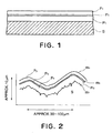
- Figure 1 is a schematic sectional view of a developer-carrying member according to the present invention, which basically includes a substrate S, and an intermediate layer P1, a joint layer P3 and a rigid electroplating layer P2 successively formed in this order on the substrate S.
- FIG. 2 is an enlarged schematic sectional view for illustrating surface roughnesses of the respective layers of the developer-carrying member shown in Figure 1.
- a curve m1 schematically represents a surface roughness distribution curve on the substrate S, which has been provided with surface unevennesses by blasting a cylindrical aluminum substrate.
- a large number of minute projections and cracks are present.
- the electroplating layer is provided with enhanced steep unevennesses affected by the minute projections and cracks on the substrate surface.
- a developer-carrying member having such surface unevennesses exhibits a lower ability of imparting charges to the developer carried thereon, and the developer is liable to fall into and stick to the steep concavities, thus soiling the developer-carrying member.
- an intermediate layer P1 has been formed on the substrate surface, and is formed by electroless plating in this embodiment to provide a smooth surface roughness curve m2, which has not been affected by the minute projections and cracks. Then, a joint layer P3 and an electroplating layer P2 are successively formed thereon to provide surface roughness curves m3 and m4, which are both characterized as smooth surface roughness curves because of the smoothness of the lower layers.
- the substrate S may have a shape corresponding to a form of developing apparatus in which the developer-carrying member is incorporated, such as a hollow cylinder (which also may be called a "sleeve"), a solid cylinder or a flat sheet.
- a hollow cylinder which also may be called a "sleeve”
- a solid cylinder which also may be called a "sleeve”
- a flat sheet such as a flat sheet.
- the developer-carrying member may suitably have an appropriate degree of surface roughness, as represented by Rz (ten point-average surface roughness) in a range of 0.3 - 7 ⁇ m or Ra (arithmetic average roughness) in a range of 0.05 - 1.1 ⁇ m.
- Rz ten point-average surface roughness
- Ra arithmetic average roughness
- the surface roughening treatment it is suitable to effect blasting with spher
- Ra and Rz described herein for indicating surface roughness are based on values measured by using a contact-type surface roughness meter ("SURFCODER SE-3300", available from K.K. Kosaka Kenkusho) under conditions of a cut-off value of 0.8 mm, a measurement length of 2.5 mm, a feed speed of 0.1 mm/s, and a magnification of 5000.
- SURFCODER SE-3300 available from K.K. Kosaka Kenkusho
- the substrate S may preferably comprise a material such as aluminum, aluminum alloy or copper alloy. These materials are non-magnetic, and suitably used in a development system utilizing a magnetic field. Further, these metal are relatively soft as represented by a Vickers hardness of 40 - 180, so that they can be easily processed by the surface roughening treatment. Moreover, because of a high thermal conductivity of 150 W/m.K or higher, they are less liable to cause heat accumulation, or a lowering in size accuracy due to thermal expansion during use.
- the intermediate layer P1 may suitably have a thickness of at least 3 ⁇ m so as to cover up the minute projections and cracks on the substrate surface, and also preferably have a thickness of at most 30 ⁇ m so as to form uniform plating layers thereon and cause an appropriate degree of surface unevennesses suitable for promoting the developer conveyance to appear on a surface of the plating layers.
- the intermediate layer P1 may suitably comprise an electroless plating layer of Ni-P, Ni-B, Pd-P, Ni-Co-P, Ni-Fe-P, Ni-W-P, Ni-Cu-P, Co-P, etc., and particularly suitably Ni-P in view of industrial applicability and stability of product quality.
- the P concentration is adjusted in a range of 5 - 15 wt. %.
- the joint layer P3 is inserted to ensure an intimate adhesion between the intermediate layer P1 and the electroplating layer P2, thereby preventing the peeling-off of the electroplating layer P2 during a long-term use of the developer-carrying member.
- the joint layer P3 comprises a substantially non-magnetic material as represented by a volume susceptibility of at most 1 ⁇ H/m.
- Preferred example of the material may include: Cu and Al.
- joint layer materials are also preferred in order to effectively suppress an internally residual stress due to a difference in thermal expansion characteristic between the intermediate layer P1 and the electroplating layer P2 formed thereon.
- volume susceptibilities of some representative materials are shown in Table A below from which the preferability of Cu and Al would be clear.
- volume susceptibility values described herein are based on values measured by using a magnetic susceptibility meter ("MPMS", made by Nippon Quantum Design K.K.) and a disk-shaped test piece having a diameter of 1.5 mm and a thickness of 60 ⁇ m.
- MPMS magnetic susceptibility meter
- the joint layer P3 may suitably be formed in a thickness of 0.2 - 2 ⁇ m. Below 0.2 ⁇ m, it becomes difficult to exhibit the function as a joint layer, and above 2 ⁇ m, a further enhanced joining effect cannot be attained but the production time and cost are increased.
- the electroplating layer P2 may suitably have a Vickers hardness Hv of at least 300, preferably at least 500.
- the electroplating layer P2 may suitably comprise Cr, Pt or Rh, particularly preferably Cr providing Hv of 600 or higher.
- the electroplating layer P2 may preferably have a thickness of at least 0.2 ⁇ m in view of the durability and a thickness of at most 5 ⁇ m in view of good surface property which is adversely affected by too large a thickness. Further, as the smooth surface shape of the intermediate layer is caused to appear also on the electroplating layer surface, it is further preferred for the electroplating layer to have a thickness of at most 1/10 of that of the intermediate layer.
- the intermediate layer P1 and the electroplating layer P2 may preferably comprise materials having volume susceptibilities of at most 5 ⁇ H/m.
- a developing apparatus 4 includes a developing sleeve 43 (developer-carrying member) which has been obtained by blasting a 32.3 mm-dia. cylindrical tube of aluminum alloy (A6063 according to JIS) with spherical glass particles of 600 mesh-pass (FGB#600) and then subjecting the cylinder to three steps of plating for providing a laminate structure as shown in Figure 1.
- a developing sleeve 43 Within the developing sleeve 43, a fixed magnet 41 having 6 magnetic poles is disposed.
- a toner (as a developer) is applied on the developing sleeve 43 in a thickness controlled by a magnetic blade 42 which is placed apart from the sleeve 43 with a gap of, e.g., 180 ⁇ m.
- the magnetic blade 42 made of, e.g., SPCC (i.e., cold-rolled steel sheet (JIS G3141), is in a form of a sheet provided with a tapered tip portion directed to the developing sleeve 43 as illustrated in Figure 6, a magnetic field formed between the magnetic blade and the developing sleeve is concentrated to a narrower region than the case of using a mere flat sheet member 242 as shown in Figure 7, thereby enhancing the thin toner layer-forming performance. As a result, a stronger toner triboelectrification ability is developed to provide a sufficient toner charge.
- the magnetic blade 42 is formed in a sheet member having a thickness t1 of 1.6 mm at its screwed root portion and a thickness t2 of 0.3 mm at its very tip portion as shown in Figure 6.
- the developing apparatus 4 is further equipped with a first stirring bar 4B and a second stirring bar 4C for stirring the toner, and a toner amount detection sensor (piezoelectric device) 44.
- the 6 magnetic poles of the fixed magnet 41 disposed within the developing sleeve 43 exhibit, e.g., the following magnetic field pattern.
- Figure 5 illustrates an embodiment of the image forming apparatus according to the invention.
- the image forming apparatus includes an a-Si (amorphous-silicon) photosensitive drum 1 of 108 mm in diameter, which is rotated at a process speed of 450 mm/sec for providing monochromatic copies of 85 A4-size sheets/min.
- An a-Si photoconductor has a dielectric constant of ca. 10 larger than an organic photoconductor (OPC) and a relatively low potential so that it is difficult to attain a sufficient latent image potential.
- OPC organic photoconductor
- an a-Si photosensitive member has a high durability providing a life of more than 3x10 6 sheets, so that it is suited for a high-speed image forming machine.
- the photosensitive member 1 is uniformly charged to, e.g., +340 volts and exposed to image light 12 at a resolution of 600 dpi.
- the image light 12 having a wavelength of, e.g., 680 nm is emitted from a semiconductor laser as a light source and illuminates the photosensitive member to lower the surface potential at an exposed part to +50 volts, thereby forming a latent image on the photosensitive member.
- laser light emitted from the laser is processed through an optical system including a collimator lens, a polygonal scanner, an f- ⁇ lens, a reflecting mirror and a dust-protection glass to provide the image light 12 which is then caused to illuminate the photosensitive drum 1 in a focused spot size on the drum which is a little larger than 42.3 ⁇ m that is one pixel size corresponding to the resolution of 600 dpi, whereby an electrostatic latent image having an exposed part potential of ca. +50 volts is formed on the drum 1.
- the electrostatic latent image is then developed with the toner from the developing apparatus 4 to form a toner image on the drum 1.
- the toner image is then positively charged with a total current of ca.
- the development is performed by using a black magnetic mono-component developer which allows a simple and highly durable developing system not requiring a maintenance until the end of the developing sleeve life.
- the detector 44 detects the absence to output a piezoelectric signal for rotating a magnet roller 9a thereby replenishing a fresh toner from a hopper 9 into the developing apparatus 4.
- the toner image formed on the drum 1 and having passed by the post charger 10 is then transferred onto a transfer material P moved in an indicated arrow direction under the action of a transfer charger 5.
- the toner image on the transfer material P is then sent to a fixing device 7 where the toner image is fixed. A portion of the toner remaining on the drum 1 after the transfer is removed from the drum 1 by a cleaner 6.
- a drum heater is generally installed with the drum 1 so as to prevent the occurrence of image flow at the time of start-up and retain a stable performance while obviating adverse effect of a temperature-dependence of the a-Si photoconductor. If the developing sleeve comprising stainless steel is used in combination with a drum equipped with a drum heater, the developing sleeve is liable to cause a thermal deformation due to a heat from the drum heater and a small thermal conductivity of the stainless steel.
- the developing sleeve may preferably comprise a material, such as aluminum or aluminum alloy, having a large thermal conductivity and less liable to cause a thermal deformation due to a heat from the drum heater.
- the developing sleeve 43 rotates at a peripheral speed of, e.g., 767.5 mm/s with a gap G1 of, e.g., 220 ⁇ m, from the photosensitive drum 1.
- the development is performed under application of a developing bias voltage to the developing sleeve 43.
- An example of the developing bias voltage suitably applied to the developing sleeve 43 is an AC/DC superposed voltage comprising an AC voltage having a peak-to-peak voltage (Vpp) of 1.0 kV, a frequency of 2.7 kHz and a duty ratio of 35 % superposed with a DC voltage (Vdc) of 280 volts.
- Vpp peak-to-peak voltage
- Vdc DC voltage
- toner suitably used in this embodiment is a magnetic toner comprising magnetic toner particles each containing magnetic fine particles dispersed in a resin.
- the toner may have a volume-average particle size of 4 - 10 ⁇ m, preferably 6 - 8 ⁇ m. Below 4 ⁇ m, the toner control becomes difficult, and particularly the solid black image portion is liable to exhibit a lower density. Above 10 ⁇ m, the resolution of thin line image is liable to be inferior. In a specific example, a toner having a volume-average particle size of 7 ⁇ m was used.
- Particle size distribution of toner particles may be measured according to various methods.
- the values described herein are based on measurement using a Coulter Counter TA-II (available from Coulter Electronics, Inc.).
- TA-II available from Coulter Electronics, Inc.
- several mg of a sample toner is dispersed in an electrolytic solution formed by adding several drops of a surfactant to a 1 %-NaCl aqueous solution, and subjecting the mixture to ultrasonic dispersion for several minutes.
- the resultant sample dispersion is subjected to a particle size distribution measurement in a particle size range of 2 - 40 ⁇ m through an aperture of 100 ⁇ m.
- a fine powder fraction of 4 ⁇ m or smaller was suppressed to 20 % or less by number, and a coarse powder fraction of 15 ⁇ m or a larger was suppressed to 5 % or less by volume.
- the toner binder may generally comprise a styrene-based polymer, such as a styrene-acrylate copolymer or a styrene-butadiene copolymer, a phenolic resin or a polyester resin.
- a styrene-based polymer such as a styrene-acrylate copolymer or a styrene-butadiene copolymer, a phenolic resin or a polyester resin.
- a 8:2 (by weight) mixture of a styrene-acrylate copolymer and a styrene-butadiene copolymer was used.
- a charge-control agent may generally be added internally to the toner particles but can also be externally blended with the toner particles. Suitable examples thereof for providing positively chargeable toners may include: nigrosine, quaternary ammonium compounds, triphenylmethane compounds and imidazole compounds. In a specific example, a triphenylmethane compound was added in an amount of 2 wt. parts per 100 wt. parts of the binder resin.
- paraffin wax was added as a wax component and magnetite particles were added as magnetic particles to provide toner particles, to which silica was externally added to provide a positively chargeable toner.
- the glass beads were blown through 4 nozzles of each 7 mm in diameter and disposed at a distance of 150 mm in 4 directions around the sleeve at a blasting pressure of 2.5 kg/cm 2 for 9 sec. (totally: 36 sec). After the blasting, the blasted sleeve surface was washed and dried to have surface roughnesses Ra of 0.6 ⁇ m and Rz of 4 ⁇ m.
- the blasted Al sleeve was treated with a commercially available zincate agent ("SUMER K-102", available from Nippon Kanizen K.K.) to surface-deposit zinc thereon for improving the adhesion of a Ni-P plating layer to be formed on the Al sleeve surface.
- SUMER K-102 commercially available zincate agent
- Ni-P electroless plating liquid available from Nippon Kanizen K.K.
- the Ni-P-plated sleeve was immersed in a plating bath containing 0.1 mol/l of copper sulfate (as a soluble copper salt), 0.3 ml/l of ethylenediamine (as a complexing agent for forming a copper complex) and 30 g/l of a surfactant ("NONION NS230", made by Nippon Yushi K.K.; for preventing pitting and providing a smooth plating film having a good appearance).
- the Cu-plating was performed at a bath temperature of ca. 30 °C at a cathode current density of 5A/dm 2 to form a 1 ⁇ m-thick Cu-plating layer as a joint layer.
- the Cu-plated sleeve was then immersed in a commercially available Cr plating liquid (aqueous chromatic acid solution) for 15 min. of electroplating at 45 °C and a current density of 15 A/dm 2 to form a 1 ⁇ m-thick Cr-plating layer.
- a commercially available Cr plating liquid aqueous chromatic acid solution
- the thus Cr-plated sleeve exhibited a coercive force of 40 oersted and a saturation magnetic flux of 60 Gauss.
- the Cr-plated sleeve exhibited a hardness Hv of 605 - 640, and surface roughnesses Ra of 0.53 ⁇ m and Rz of 3.54 ⁇ m.
- a magnet characterized by the data shown in the above Table 1 was inserted in the above-treated sleeve to provide a developing sleeve.
- the above-prepared developing sleeve was incorporated in a developing apparatus as described above with reference to Figure 4 (including a magnetic blade 42 having a tapered tip as described with reference to Figure 6 and disposed with a gap G2 of 180 ⁇ m from the developing sleeve), and the developing apparatus was incorporated in an image forming system described with reference to Figure 5, to evaluate image forming performances, particularly the tailing suppression performance.
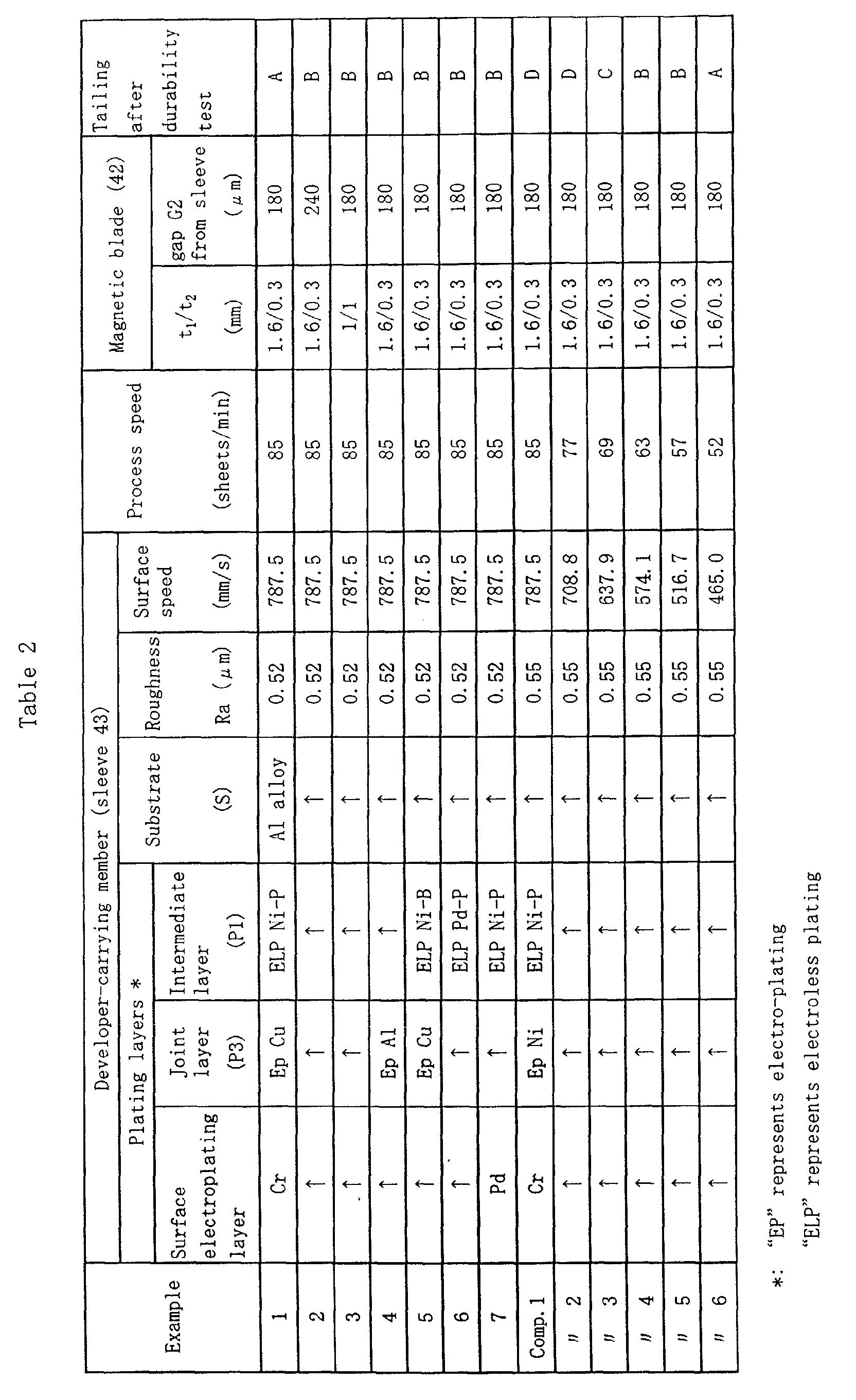
- an original having an image-areal percentage of 6 % was continually reproduced on both sides each of 10 6 A4-size sheets laterally fed at a rate of ca. 6x10 4 pages/day (including 12 hours of operation each day) in an environment of 23 °C/50 %RH, and after the continual image formation, a lateral line having a width of 4 dots (as illustrated in Figure 3A) was reproduced, and the reproduced lateral line image was evaluated with respect to the presence or absence of tailing of images as illustrated in Figure 3B according to the following standard.
- a developing sleeve was prepared and evaluated in the same manner as in Example 1 except that the spacing between the magnetic blade 42 and the sleeve 43 was increased from 180 ⁇ m to 240 ⁇ m.
- a developing sleeve was prepared and evaluated in the same manner as in Example 1 except that the joint layer was formed by electroplating of aluminum by using a plating both containing AlCl 3 and 1-methyl-3-propylimidazolium bromide in a mol ratio of 2:1 and containing 4 g/l of polystyrene under stirring.
- the sleeve was subjected to pre-treatment including: degreasing with an alkali, electrolytic washing, acid washing, water washing and drying.
- An aluminum sheet was immersed as the anode and the Ni-P-plated sleeve was immersed as the cathode for 2.5 min. in the plating bath held at 50 °C under stirring in a dry nitrogen gas atmosphere to effect aluminum plating at a current density of 1 A/dm 2 .
- a developing sleeve was prepared and evaluated in the same manner as in Example 1 except that the intermediate layer was formed as a 19 ⁇ m-thick Pd-P electroless plating layer by using a plating bath at pH 7 and 50 °C having the following composition: Palladium chloride 1.5 g/l Ethylenediamine 5 " Sodium hydrophophite 7 " Thioglycolic acid 0.03 "
- a developing sleeve was prepared and evaluated in the same manner as in Example 1 except that the surfacemost electroplating layer was a 1.5 ⁇ m-thick principally Pd-electroplating layer by electroplating for 20 sec. at a current density of 2A/dm 2 in a Pd-plating bath at pH 7 and 50 °C under stirring having the following composition: Dichlorotetraamine-palladium 4 g/l Pyridine-3-sulfonic acid 5 " Thallium nitrate 27 ppm Ammonium nitrate 400 g/l Ammonium chloride 107 "
- a developing sleeve was prepared in the same manner as in Example 1 except that a 1 ⁇ m-thick Ni electroplating layer instead of the Cu electroplating layer was formed by immersing the Ni-P plated Al sleeve in an Ni-plating liquid (sulfuric acid-acidified nickel sulfate aqueous) for electroplating.
- Ni-plating liquid sulfuric acid-acidified nickel sulfate aqueous
Landscapes
- Physics & Mathematics (AREA)
- General Physics & Mathematics (AREA)
- Dry Development In Electrophotography (AREA)
- Magnetic Brush Developing In Electrophotography (AREA)
Abstract
Description
| Volume susceptibility (µH/m) | ||||
| Al | Co | Cr | Cu | Ni |
| 0.61 | 144000 | 3.2 | -0.086 | 49000 |
| Pole | Magnetic force (G) | Angle (deg.) |
| N1 | 1000 | 0 |
| N2 | 1000 | 120 |
| N3 | 600 | 220 |
| S1 | 900 | 60 |
| S2 | 500 | 175 |
| S3 | 700 | 270 |
| Palladium chloride | 1.5 g/ |
| Ethylenediamine | |
| 5 " | |
| | 7 " |
| Thioglycolic acid | 0.03 " |
| Dichlorotetraamine-palladium | 4 g/l |
| Pyridine-3- | 5 " |
| Thallium nitrate | 27 ppm |
| Ammonium nitrate | 400 g/l |
| Ammonium chloride | 107 " |
Claims (22)
- A developer-carrying member for carrying and conveying thereon a developer, having a laminate structure including successively a substrate having a surface roughness, an intermediate layer having a surface roughness smaller than that of the substrate, a joint layer and an electroplating layer, wherein the joint layer comprises a material having a volume susceptibility of at most 1 µH.m-1.
- A developer-carrying member according to Claim 1, wherein the substrate has a surface roughness as represented by a ten point-average roughness Rz of 1 - 8 µm or an arithmetic average roughness Ra of 0.1 - 1.2 µm.
- A developer-carrying member according to Claim 1 or Claim 2, wherein the substrate comprises a material selected from aluminum, aluminum alloy or copper alloy, and having a Vickers hardness of 40 - 180.
- A developer-carrying member according to any preceding claim wherein the intermediate layer has a thickness of 3 - 30 µm.
- A developer-carrying member according to any preceding claim wherein the intermediate layer is an Ni-P electroless plating layer.
- A developer-carrying member according to any preceding claim wherein the electroplating layer has a thickness of 0.2 - 5 µm.
- A developer-carrying member according to any preceding claim wherein the electroplating layer has a thickness smaller than that of the intermediate layer.
- A developer-carrying member according to any preceding claim wherein the joint layer comprises a Cu plating layer or an Al plating layer.
- A developer-carrying member according to any preceding claim wherein the joint layer has a thickness of 0.2 - 2 µm.
- A developer-carrying member according to any preceding claim wherein the electroplating layer comprises a Cr plating layer.
- A developer-carrying member according to any preceding claim wherein the intermediate layer comprises an Ni-P electroless plating layer, and the electroplating layer comprises a Cr plating layer.
- A developer-carrying member according to Claim 11, wherein the joint layer comprises a Cu plating layer.
- A developing apparatus for developing an electrostatic latent image formed on an image-bearing member, the developing apparatus comprising a developer-carrying member which has a laminate structure including successively a substrate having a surface roughness, an intermediate layer having a surface roughness smaller than that of the substrate, a joint layer and an electroplating layer, wherein the joint layer comprises a material having a volume susceptibility of at most 1 µH.m-1.
- A developing apparatus according to Claim 13, wherein the substrate of the developer-carrying member comprises a hollow cylindrical substrate, within which a magnetic field generating means is disposed.
- An image forming apparatus, comprising: an image-bearing member for forming an electrostatic image thereon, and a developer-carrying member disposed opposite to the image-bearing member for carrying and conveying a developer thereon to develop the electrostatic image, wherein the developer-carrying member has a laminate structure including successively a substrate having a surface roughness, an intermediate layer having a surface roughness smaller than that of the substrate, a joint layer and an electroplating layer, wherein the joint layer comprises a material having a volume susceptibility of at most 1 µH.m-1.
- An image forming apparatus apparatus according to Claim 15, wherein the substrate of the developer-carrying member comprises a hollow cylindrical substrate, within which a magnetic field generating means is disposed.
- An image forming apparatus according to Claim 16, wherein the developer-carrying member is driven in rotation at a peripheral speed of at least 570 mm/sec.
- An image forming apparatus according to Claim 15, wherein the electrostatic image-bearing member has a photosensitive layer principally comprising amorphous silicon.
- A developing apparatus according to claim 13 or claim 14 further comprising a developer-carrying member having the features of any one of claims 2 to 12.
- An image forming apparatus according to any one of claims 15 to 18 further comprising a developer-carrying member having the features of any one of claims 2 to 12.
- A method of manufacturing a developer-carrying member comprising the steps of:wherein the joint layer comprises a material having a volume susceptibility of at most 1µH.m-1.(a) providing a substrate having a surface roughness;(b) applying an intermediate layer to said substrate, said intermediate layer having a surface roughness less than that of the substrate;(c) applying a joint layer to said intermediate layer, and(d) applying an electroplating layer to the joint layer;
- A method as claimed in claim 21 wherein the respective layers of the developer-carrying member have the features of any one of claims 2 to 12.
Applications Claiming Priority (2)
| Application Number | Priority Date | Filing Date | Title |
|---|---|---|---|
| JP2001050219 | 2001-02-26 | ||
| JP2001050219 | 2001-02-26 |
Publications (3)
| Publication Number | Publication Date |
|---|---|
| EP1235119A2 true EP1235119A2 (en) | 2002-08-28 |
| EP1235119A3 EP1235119A3 (en) | 2005-12-14 |
| EP1235119B1 EP1235119B1 (en) | 2013-07-24 |
Family
ID=18911214
Family Applications (1)
| Application Number | Title | Priority Date | Filing Date |
|---|---|---|---|
| EP02251343.6A Expired - Lifetime EP1235119B1 (en) | 2001-02-26 | 2002-02-26 | Developer-carrying member, and developing apparatus and image forming apparatus including the member |
Country Status (2)
| Country | Link |
|---|---|
| US (1) | US6795675B2 (en) |
| EP (1) | EP1235119B1 (en) |
Cited By (1)
| Publication number | Priority date | Publication date | Assignee | Title |
|---|---|---|---|---|
| CN100474130C (en) * | 2004-09-30 | 2009-04-01 | 京瓷美达株式会社 | Magnetic mono-component toner for developing electrostatic latent image and image forming method |
Families Citing this family (5)
| Publication number | Priority date | Publication date | Assignee | Title |
|---|---|---|---|---|
| US7840145B2 (en) * | 2003-06-27 | 2010-11-23 | The Boeing Company | Apparatus and methods for noise-feedback controlled optical systems |
| US8274160B2 (en) | 2003-08-21 | 2012-09-25 | Intersil Americas Inc. | Active area bonding compatible high current structures |
| US7005369B2 (en) * | 2003-08-21 | 2006-02-28 | Intersil American Inc. | Active area bonding compatible high current structures |
| US20050221112A1 (en) * | 2004-03-31 | 2005-10-06 | Daewoong Suh | Microtools for package substrate patterning |
| JP4373462B2 (en) * | 2007-08-03 | 2009-11-25 | 住友ゴム工業株式会社 | Member for image forming apparatus |
Family Cites Families (13)
| Publication number | Priority date | Publication date | Assignee | Title |
|---|---|---|---|---|
| JPS5526526A (en) | 1978-08-15 | 1980-02-26 | Hitachi Metals Ltd | Magnet roll |
| JPS58132768A (en) | 1982-02-03 | 1983-08-08 | Hitachi Metals Ltd | Developing device |
| JPH0760278B2 (en) | 1986-08-30 | 1995-06-28 | キヤノン株式会社 | Electrophotographic device |
| JPH0284679A (en) * | 1988-04-15 | 1990-03-26 | Canon Inc | developing device |
| JPH0341485A (en) | 1989-07-07 | 1991-02-21 | Kanegafuchi Chem Ind Co Ltd | Developing roller |
| DE69123420T2 (en) * | 1990-09-28 | 1997-04-03 | Canon Kk | Device for developing electrostatic latent images and developing rollers therefor |
| JPH06230676A (en) | 1993-02-03 | 1994-08-19 | Konica Corp | Development device |
| CA2213203A1 (en) * | 1995-02-17 | 1996-08-22 | Sheldon Lee Roderick | Electroless plated magnetic brush roller for xerographic copiers, printers and the like |
| US5697029A (en) * | 1995-04-11 | 1997-12-09 | Bridgestone Corporation | Magnet developing roller with dry plated sleeve |
| EP1324151B1 (en) * | 1997-01-31 | 2008-02-20 | Seiko Epson Corporation | Developing unit |
| US6104903A (en) * | 1997-10-08 | 2000-08-15 | Canon Kabushiki Kaisha | Developing device |
| JPH11194618A (en) * | 1997-11-10 | 1999-07-21 | Canon Inc | Image forming device |
| JP3588563B2 (en) | 1999-03-31 | 2004-11-10 | キヤノン株式会社 | Developer carrying member, developing device and image forming apparatus using the same |
-
2002
- 2002-02-25 US US10/080,670 patent/US6795675B2/en not_active Expired - Fee Related
- 2002-02-26 EP EP02251343.6A patent/EP1235119B1/en not_active Expired - Lifetime
Cited By (1)
| Publication number | Priority date | Publication date | Assignee | Title |
|---|---|---|---|---|
| CN100474130C (en) * | 2004-09-30 | 2009-04-01 | 京瓷美达株式会社 | Magnetic mono-component toner for developing electrostatic latent image and image forming method |
Also Published As
| Publication number | Publication date |
|---|---|
| US20020168201A1 (en) | 2002-11-14 |
| EP1235119A3 (en) | 2005-12-14 |
| US6795675B2 (en) | 2004-09-21 |
| EP1235119B1 (en) | 2013-07-24 |
Similar Documents
| Publication | Publication Date | Title |
|---|---|---|
| EP1041450B1 (en) | Developer-carrying member, and developing device and image forming apparatus including the member | |
| JP4732536B2 (en) | Development device | |
| US5286917A (en) | Apparatus for developing electrostatic latent image and developing roller therefor | |
| EP0915393A2 (en) | Developer bearing body electroless plated on blasted surface using spherical particles, production method therefor and developing apparatus using the same | |
| US6430384B2 (en) | Developer-carrying member having exposed surface containing graphite or molybdenum disulfide particles | |
| US6546222B2 (en) | Developing apparatus | |
| JPS58132768A (en) | Developing device | |
| EP1235119B1 (en) | Developer-carrying member, and developing apparatus and image forming apparatus including the member | |
| JP4545990B2 (en) | Development device | |
| JP3262466B2 (en) | Developing sleeve and developing device | |
| JP4378143B2 (en) | Development device | |
| JP2001100531A (en) | Developing device for electrophotography | |
| JP3990922B2 (en) | Developer carrying member and image forming apparatus using the same | |
| US20040223789A1 (en) | Developing apparatus | |
| JP4939118B2 (en) | Image forming apparatus | |
| JP2000206776A (en) | Developing device | |
| JP2003005504A (en) | Developer carrier and developing device using the same | |
| JP2003076132A (en) | Developer carrying member, developing device, and image forming device | |
| JP5802395B2 (en) | Developing roller, developing device, developing method, and image forming apparatus | |
| JP2002351208A (en) | Developing device | |
| JP2000267426A (en) | Developing device and image forming device | |
| JP3352412B2 (en) | Developing device | |
| JPH08160739A (en) | Developing sleeve and developing device | |
| JP2001142296A (en) | Developing device | |
| JP5173127B2 (en) | Development device |
Legal Events
| Date | Code | Title | Description |
|---|---|---|---|
| PUAI | Public reference made under article 153(3) epc to a published international application that has entered the european phase |
Free format text: ORIGINAL CODE: 0009012 |
|
| AK | Designated contracting states |
Kind code of ref document: A2 Designated state(s): AT BE CH CY DE DK ES FI FR GB GR IE IT LI LU MC NL PT SE TR |
|
| AX | Request for extension of the european patent |
Free format text: AL;LT;LV;MK;RO;SI |
|
| PUAL | Search report despatched |
Free format text: ORIGINAL CODE: 0009013 |
|
| AK | Designated contracting states |
Kind code of ref document: A3 Designated state(s): AT BE CH CY DE DK ES FI FR GB GR IE IT LI LU MC NL PT SE TR |
|
| AX | Request for extension of the european patent |
Extension state: AL LT LV MK RO SI |
|
| RIC1 | Information provided on ipc code assigned before grant |
Ipc: 7G 03G 15/09 A Ipc: 7G 03G 15/08 B |
|
| 17P | Request for examination filed |
Effective date: 20060614 |
|
| AKX | Designation fees paid |
Designated state(s): DE FR GB IT |
|
| 17Q | First examination report despatched |
Effective date: 20060823 |
|
| GRAP | Despatch of communication of intention to grant a patent |
Free format text: ORIGINAL CODE: EPIDOSNIGR1 |
|
| RIN1 | Information on inventor provided before grant (corrected) |
Inventor name: FUJITA, HIDEKI, C/O CANON KABUSHIKI KAISHA |
|
| GRAS | Grant fee paid |
Free format text: ORIGINAL CODE: EPIDOSNIGR3 |
|
| GRAA | (expected) grant |
Free format text: ORIGINAL CODE: 0009210 |
|
| AK | Designated contracting states |
Kind code of ref document: B1 Designated state(s): DE FR GB IT |
|
| REG | Reference to a national code |
Ref country code: GB Ref legal event code: FG4D |
|
| REG | Reference to a national code |
Ref country code: DE Ref legal event code: R096 Ref document number: 60245274 Country of ref document: DE Effective date: 20130912 |
|
| PG25 | Lapsed in a contracting state [announced via postgrant information from national office to epo] |
Ref country code: IT Free format text: LAPSE BECAUSE OF FAILURE TO SUBMIT A TRANSLATION OF THE DESCRIPTION OR TO PAY THE FEE WITHIN THE PRESCRIBED TIME-LIMIT Effective date: 20130724 |
|
| PLBE | No opposition filed within time limit |
Free format text: ORIGINAL CODE: 0009261 |
|
| STAA | Information on the status of an ep patent application or granted ep patent |
Free format text: STATUS: NO OPPOSITION FILED WITHIN TIME LIMIT |
|
| 26N | No opposition filed |
Effective date: 20140425 |
|
| REG | Reference to a national code |
Ref country code: DE Ref legal event code: R097 Ref document number: 60245274 Country of ref document: DE Effective date: 20140425 |
|
| REG | Reference to a national code |
Ref country code: FR Ref legal event code: PLFP Year of fee payment: 14 |
|
| PGFP | Annual fee paid to national office [announced via postgrant information from national office to epo] |
Ref country code: DE Payment date: 20150228 Year of fee payment: 14 |
|
| PGFP | Annual fee paid to national office [announced via postgrant information from national office to epo] |
Ref country code: GB Payment date: 20150220 Year of fee payment: 14 Ref country code: FR Payment date: 20150227 Year of fee payment: 14 |
|
| REG | Reference to a national code |
Ref country code: DE Ref legal event code: R119 Ref document number: 60245274 Country of ref document: DE |
|
| GBPC | Gb: european patent ceased through non-payment of renewal fee |
Effective date: 20160226 |
|
| REG | Reference to a national code |
Ref country code: FR Ref legal event code: ST Effective date: 20161028 |
|
| PG25 | Lapsed in a contracting state [announced via postgrant information from national office to epo] |
Ref country code: FR Free format text: LAPSE BECAUSE OF NON-PAYMENT OF DUE FEES Effective date: 20160229 Ref country code: GB Free format text: LAPSE BECAUSE OF NON-PAYMENT OF DUE FEES Effective date: 20160226 Ref country code: DE Free format text: LAPSE BECAUSE OF NON-PAYMENT OF DUE FEES Effective date: 20160901 |