EP1233473A2 - Phased array beamformer module driving two elements - Google Patents
Phased array beamformer module driving two elements Download PDFInfo
- Publication number
- EP1233473A2 EP1233473A2 EP02003755A EP02003755A EP1233473A2 EP 1233473 A2 EP1233473 A2 EP 1233473A2 EP 02003755 A EP02003755 A EP 02003755A EP 02003755 A EP02003755 A EP 02003755A EP 1233473 A2 EP1233473 A2 EP 1233473A2
- Authority
- EP
- European Patent Office
- Prior art keywords
- beamformer
- circuitry
- module
- groups
- twelve
- Prior art date
- Legal status (The legal status is an assumption and is not a legal conclusion. Google has not performed a legal analysis and makes no representation as to the accuracy of the status listed.)
- Granted
Links
Images



Classifications
-
- H—ELECTRICITY
- H01—ELECTRIC ELEMENTS
- H01Q—ANTENNAS, i.e. RADIO AERIALS
- H01Q25/00—Antennas or antenna systems providing at least two radiating patterns
-
- H—ELECTRICITY
- H01—ELECTRIC ELEMENTS
- H01Q—ANTENNAS, i.e. RADIO AERIALS
- H01Q21/00—Antenna arrays or systems
- H01Q21/0006—Particular feeding systems
- H01Q21/0025—Modular arrays
Definitions
- the present invention generally relates to antennas and, more particularly, to phased array antennas.
- Phased array antennas are generally composed of an array of radiating elements coupled to a signal input source through a number of identical beamformer modules.
- the beamformer modules are connected to the antenna main signal source and to the antenna frame through a wave guide interface surface so as to form a parallel stack of beamformer modules on the wave guide interface surface.
- a certain number of modules are arranged in equidistant parallel stacks which are perpendicularly connected to each wave guide interface surface.
- each radiating element is connected to a top end of each beamformer module and thereby form a subarray of radiating elements.
- the array of radiating elements forms the top end of the antenna.
- the radiating elements individually or in the form of subarrays provide a directed beam of electromagnetic signals such as radio frequency (RF) signals.
- Each module contains phase shifter circuitry having phase shifter elements to control the phase of the inputted signals. By shifting the phase of the inputted signals in each phase shift element, the direction of the antenna beam can be changed without needing to mechanically move the antenna.
- the number of phase shifter elements per array module determines the number of beams that an antenna can generate and thus the RF throughput of the antenna.
- the radiating elements Due to the strict design constraints on the dimensions of the radiating elements and the modules of an antenna, it is necessary to match the planar area occupied by the upper edge of a subbarray of radiating elements with the area of a wave guide interface surface. In other words, the projection of the planar area occupied by the radiating elements onto the interface surface defines the area that a module of the radiating element is permitted to occupy. Since the radiating elements follow strict dimensional limitations, this situation limits the size of the beamformer modules and hence the number of phase shifter elements per module, which in turn limits the number of beams that can be generated using a single module.
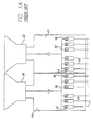
- FIGS. 1A and 1B illustrate two prior art beamformer modules 10 and 12, each having six phase shifters 14.
- the phase shifters 14 are connected to signal source input lines 16 extending between input connectors 17 and the phase shifters 14.
- the output wiring 18 from the phase shifters 14 is connected to radiating elements 20 and 22 which are coupled to top ends of the modules 10 and 12 respectively.
- the modules 10 and 12 with the radiating elements 20 and 22 are placed on top of a wave guide interface surface 24 shown in FIG. 1B.
- the interface surface 24 has eight rows 26 having twelve input connection slots 28 to receive input connectors 17 of the modules 10, 12.
- a first group 30 of slots 28 receives the module 10 and the second group 32 of slots 28 receives the module 12.
- the other slots 28 are filled in with a similar side-by-side placement method.
- the first beamformer module is coupled to at least two radiating elements.
- the first beam former module comprises at least two groups of beamforming circuitry on a primary plane of the first beamformer module and at least one feeder line extending from each beamforming circuit. Each feeder line is coupled to one of the radiating elements to transmit an output of each beam forming circuit.
- the second beamformer module is also coupled to at least two radiating elements.
- the second beam former module comprises at least two groups of beamforming circuitry on a primary plane of the second beamformer module and at least one feeder line extending from each beamforming circuitry. Each feeder line is coupled to one of the radiating elements to transmit an output of each beam forming circuitry.
- the dual module system of the present invention increases the number of beams generated from a phased array antenna device.
- the beams to be implemented are increased in the dual module system and the corresponding radiating element array row.
- This system doubles the number of beams in comparison to the above given prior art system.
- the planar surface area occupied by the array elements and the area of the wave guide interface surface are generally in a one-to-one dimensional agreement.
- the modules of an array row of two radiating elements can only be coupled onto a designated row area on the interface surface of a wave guide power splitter which is connected to the antenna input sources.
- a typical phased array antenna features one beamformer module per radiating element, and the design constraints for the radiating elements places the modules in a side-by-side configuration on a designated section of the wave guide interface surface.
- a typical radiating element covers a 2"x2" square area, and two radiating elements cover a 2"x4" rectangular area.
- the designated area required for the modules of the radiating elements is limited to an area of 2"x4".
- This conventional approach limits the size of the modules and the amount of circuitry they can have. This, in turn, restricts the number of RF beams that can be generated in a single radiating element to less than half the number that can be implemented using the present invention.
- the dual module system of the present invention comprises two beamformer modules that are a right hand circular polarization beamformer and a left hand circular polarization beamformer.
- the left and right hand beamformers are mounted onto a single row on the interface surface and adjacent to each other. Both beamformers drive two beam-radiating elements in an array of a plurality of beam radiating elements.
- each beamformer module is equipped with twenty-four channels of MMIC (monolithic microwave integrated circuit) amplitude and phase weighting circuits driving two array element SSPAs (solid state power amplifier). Again, in each beamformer of the system, the twenty-four channels are arranged in two groups of twelve, one group for each array element or radiating element.
- MMIC monolithic microwave integrated circuit
- SSPAs solid state power amplifier
- Each of twelve module beam inputs is split into two, one for each array element resulting in a total of twelve beam inputs as opposed to the prior art six beam inputs to a singe radiating element.
- both beamformers share the same space designated for two radiating elements in two array rows.
- the dual module system doubles the number of beams fed to each radiating element in a phased array antenna system.
- the width of the modules may be increased, allowing the beamformer implementation to move from a high loss but more compact implementation such as strip-line to a larger but lower loss implementation such as a wave guide. This reduces the RF losses of the beamformer circuitry.
- the insertion loss of the RF beamforming network is reduced by 4 to 6 dB, allowing a reduction in input RF drive power to 25 - 40 % of that required for the prior state of the art.
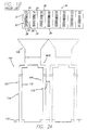
- FIGS. 2A-2E show the dual module system 100, or dual element beamformer module, of the present invention.
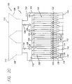
- the dual module system 100 comprises a first beamformer module 102 (FIG. 2B) and a second beamformer module 104 (FIG. 2C) which is interlaced with the first module 102.
- each module generally has the same size, shape, and circuitry as the other. The difference is that the circular polarization of the circuitry on the first module 102 is opposite to the circular polarization of the circuitry of the second module 104.
- a dual radiating element 105 comprises first and second radiating elements 106 and 108 which are secured on an upper or first portion 109 of the system 100 and electrically connected to the modules 102 and 104.
- the dual radial element 105 defines a top planar area 110 that is the planar area defined by the top peripheral edge 111 of the dual element 105.
- the modules 102 and 104 further comprise a primary surface 112 or RF (radio frequency) side and a secondary surface 114 or DC (direct current) side (FIG, 2D).
- the dual module system 100 is secured to an interface surface 116 (FIGS. 3A-3B).
- the primary surfaces 112 of the first and second modules 102 and 104 respectively comprise beamformer circuits or beamformers 118 and 120, preferably MMIC (monolithic microwave integrated circuit) amplitude and phase weighting circuits.
- the first module 104 may be polarized with right hand circular polarization and, accordingly, the beamformer 118 can be referred to as a right-hand circular polarization beamformer (RHCP).
- the beamformer 120 for the second module 104 may be polarized with left-hand circular polarization and, accordingly, the beamformer 120 can be referred to as a left-hand circular polarization beamformer (LHCP).
- Each beamformer 118, 120 comprises a plurality of phase shift-elements 122.
- each beamformer 118, 120 comprises twenty-four channels of MMIC amplitude and phase weighting circuits 122 or phase shift elements.
- phased array antenna systems generate signals of opposite polarization (RHCP and LHCP) to maximize data transmitted or received in a given amount of assigned frequency spectrum. This approach allows two sets of user beams to share the same frequency spectrum without interference. It is thus necessary to assign user beams to each polarization and provide these composite RF signals to each radiating element of the array.
- a radiating element is designed with separate input ports for each polarization. As shown in FIGS.
- phase shift elements 122 are connected to a first circuitry 124 and another twelve of them are connected to a second circuitry 126.
- the first circuitry 124 drives a first amplifier 128 of the first radiating element 106 while the second circuitry 126 drives a second amplifier 129 of the second radiating element 108.
- the amplifiers 128 and 129 are respectively connected to output lines 130 and 131 of the phase shifters 122 in the first and the second circuits 124 and 126.
- the amplifiers 128 and 129 are connected to the radiating elements 106 and 108 via a first feeder line 132 and a second feeder 134, respectively.
- twelve beam input lines 136 are split into first and second input lines 138 and 140 to provide beam input for each radiating element 106 and 108 .
- the input lines 138 provide beam input for the phase shifters 122 in the first circuitry 124 and the input lines 140 provide beam input for the phase shifters 122 in the second circuit.
- input lines 136 are connected to input ports 142 located at lower ends 144 of the modules 102 and 104, where the dual module system 100 is secured to the interface surface 116.
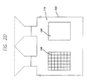
- FIG. 2D shows the secondary or DC side 114 of one of the beamformer modules 102 or 104, for example the beamformer module 102.
- the secondary sides 114 of the modules comprise substantially identical features. Therefore, for the purpose of clarity, such features will be described using the secondary side 114 of the first module 102.
- the DC side 114 comprises a number of control circuitry 146, which may preferably be application specific integrated circuits (ASICs). ASICs 146 provide control signals to the phase shifter MMICs 122.
- ASICs 146 application specific integrated circuits
- FIG. 3A shows the wave guide interface surface 116 where the beamformer module of the invention is connected to a waveguide power splitter 147 shown in FIG. 3B.
- the interface surface 116 is partitioned into a plurality of dual module sections 148 to connect a plurality of the dual module systems 100 of the present invention.
- the interface surface 116 comprises eight dual module sections 148.
- the sections 148 are sized and shaped to match the top planar area 110 defined by the dual element 105 (FIGS. 2B and 4) which may be generally rectangular in shape.
- Each section 148 allows one way input signal to the corresponding dual module systems. Therefore, in this embodiment, each wave guide power splitter 147 comprises eight ways.
- the sections 148 are sized to have 2"x4" dimensions.
- both beamformer modules 102 and 104 share the same space designated for two radiating elements. The dual module system thereby doubles the number of beams to be fed to radiating elements in a given phased array antenna system.
- Each dual module section 148 comprises a number of waveguide openings 150 configured as two parallel rows, namely a first opening row 152 and a second opening row 154.
- the wave guide openings 150 form the input channels of the wave guide power splitter 147.
- each opening row 152, 154 comprises twelve waveguide openings 150 to receive twelve input ports 142 of the beamformer modules 102 and 104.
- the wave guide power splitter 147 may be referred to as a twenty-four channel, eight-way power splitter which can drive sixteen of the radiating elements 106, 108 or eight of the dual elements 105.
- the input ports 142 of the first beamformer module 102 may be coupled with the openings 150 in the first row 152 while the input ports 142 of the second beam former module 104 may be coupled with the openings 150 in the second row 154.
- the first and second beamformer modules 102, 104 may be substantially parallel to one another and both may be substantially perpendicular to the interface surface 116. Accordingly, a plurality of dual element systems 100 can be mounted in similar fashion to form a phased array antenna.
- a beam signal can be inputted into the dual module system 100 through the wave guide power splitter 147.
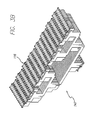
- a partially assembled phased array antenna shows eight of the dual radiating elements 105 assembled on top of eight of the dual module systems 100 which are, in turn, mounted on the wave guide power splitter 147 of the phased array antenna 160.
- a modular beamformer system for providing signals to at least two radiating elements of a phased array antenna.
- the system includes a right-hand circular polarization beamformer module and a left-hand circular polarization beamformer module.
- the left and right circular polarization beamformer modules are coupled to two radiating elements.
- Each beamformer module includes two groups of beamforming circuitry, one per radiating element.
- At least one feeder line extends from each beamforming circuitry and is coupled to one of the radiating elements to transmit an output of each beamforming circuitry.
Landscapes
- Variable-Direction Aerials And Aerial Arrays (AREA)
Abstract
Description
Claims (17)
- A modular beamformer system for providing signals to at least two radiating elements (106, 108) of a phased array antenna (160),
characterized bya first beamformer module (102) coupled to at least two radiating elements (106, 108), wherein the first beamformer module (102) comprises:at least two first groups of beamforming circuitry (124, 126) on a primary plane (112) of the first beamformer module (102); andat least one first feeder line (132) extending from the at least two first groups of beamforming circuitry (124, 126), the at least one first feeder line (132) coupled to one of the radiating elements (106, 108) to transmit an output from the at least two first groups of beamforming circuitry (124, 126);a second beamformer module (104) coupled to the at least two radiating elements (106, 108), wherein the second beamformer module (104) comprises:at least two second groups of beamforming circuitry (124, 126) on a primary plane (112) of the second beamformer module (104); andat least one second feeder line (134) extending from the at least two second groups of beamforming circuitry (124, 126), the at least one second feeder line (134) coupled to one of the radiating elements (106, 108) to transmit an output from the at least two second groups of beamforming circuitry (124, 126). - The system of claim 1, characterized in that the first and second beamformer modules (102, 104) form a dual beamformer module (100) to drive the at least two radiating elements (106, 108).
- The system of claim 2, characterized in that the dual beamformer module (100) is coupled to an interface (116) of a waveguide power splitter (147) of the phased array antenna (160).
- The system of any of claims 1-3, characterized in that at least one of the first and second groups of beamforming circuitry (124, 126) comprises phase shift elements (122).
- The system of claim 4, characterized in that the phase shift elements (122) comprise MMIC amplitude and phase weighting circuits.
- The system of any of claims 1-5, characterized in that the at least two first groups of beamforming circuitry (124, 126) of the first beamformer module (102) comprise right-hand circular polarization.
- The system of any of claims 1-6, characterized in that the at least two second groups of beamforming circuitry (124, 126) of the second beamformer module (104) comprise left-hand circular polarization.
- The system of any of claims 1-7, characterized in that the at least two first groups of beamforming circuitry comprise a first circuitry (124) and a second circuitry (126).
- The system of claim 8, characterized in that the first circuitry (124) comprises a first predetermined number of phase shift elements (122).
- The system of claim 8 or 9, characterized in that the second circuitry (126) comprises a second predetermined number of phase shift elements (122).
- The system of claim 9 and 10, characterized in that the first and the second predetermined numbers each equal twelve.
- The system of any of claims 8-11, characterized in that the first beamforming circuitry (124) comprises twelve first input lines (138) connected to a group of twelve input ports of the wave guide power splitter (147).
- The system of claim 3 and any of claims 8-12, characterized in that the second beamforming circuitry (126) comprises twelve second input lines (140) connected to the group of twelve input ports of the wave guide power splitter (147).
- The system of claim 12 or 13, characterized in that the twelve first input lines (138) are connected to twelve first phase shift elements (122) in the first beamforming circuitry (124) on a one phase shift element per input line basis.
- The system of claim 13 or 14, characterized in that the twelve second input lines (140) are connected to twelve second phase shift elements (122) in the second beam forming circuitry (126) on a one phase shift element per input line basis.
- The system of any of claims 1-15, characterized in that the first beamformer module (102) comprises at least two first amplifiers (128) coupled to the at least one first feeder line (132).
- The system of any of claims 1-16, characterized in that the second beamformer module (104) comprises at least two second amplifiers (129) coupled to the at least one second feeder line (134).
Applications Claiming Priority (2)
| Application Number | Priority Date | Filing Date | Title |
|---|---|---|---|
| US790245 | 2001-02-20 | ||
| US09/790,245 US6366238B1 (en) | 2001-02-20 | 2001-02-20 | Phased array beamformer module driving two elements |
Publications (3)
| Publication Number | Publication Date |
|---|---|
| EP1233473A2 true EP1233473A2 (en) | 2002-08-21 |
| EP1233473A3 EP1233473A3 (en) | 2003-07-30 |
| EP1233473B1 EP1233473B1 (en) | 2006-04-26 |
Family
ID=25150076
Family Applications (1)
| Application Number | Title | Priority Date | Filing Date |
|---|---|---|---|
| EP02003755A Expired - Lifetime EP1233473B1 (en) | 2001-02-20 | 2002-02-19 | Phased array beamformer module driving two elements |
Country Status (3)
| Country | Link |
|---|---|
| US (1) | US6366238B1 (en) |
| EP (1) | EP1233473B1 (en) |
| DE (1) | DE60210844T2 (en) |
Families Citing this family (174)
| Publication number | Priority date | Publication date | Assignee | Title |
|---|---|---|---|---|
| US6703976B2 (en) * | 2001-11-21 | 2004-03-09 | Lockheed Martin Corporation | Scaleable antenna array architecture using standard radiating subarrays and amplifying/beamforming assemblies |
| DE60224849T2 (en) * | 2002-04-30 | 2009-01-22 | Nokia Corp. | METHOD AND DEVICE FOR MANAGING TREE DATA EXCHANGE |
| US6738017B2 (en) | 2002-08-06 | 2004-05-18 | Lockheed Martin Corporation | Modular phased array with improved beam-to-beam isolation |
| US20040196203A1 (en) * | 2002-09-11 | 2004-10-07 | Lockheed Martin Corporation | Partly interleaved phased arrays with different antenna elements in central and outer region |
| US7050019B1 (en) | 2002-09-11 | 2006-05-23 | Lockheed Martin Corporation | Concentric phased arrays symmetrically oriented on the spacecraft bus for yaw-independent navigation |
| US6992638B2 (en) * | 2003-09-27 | 2006-01-31 | Paratek Microwave, Inc. | High gain, steerable multiple beam antenna system |
| EP1825568A1 (en) * | 2004-12-13 | 2007-08-29 | TELEFONAKTIEBOLAGET LM ERICSSON (publ) | An antenna arrangement and a method relating thereto |
| US10009065B2 (en) | 2012-12-05 | 2018-06-26 | At&T Intellectual Property I, L.P. | Backhaul link for distributed antenna system |
| US9113347B2 (en) | 2012-12-05 | 2015-08-18 | At&T Intellectual Property I, Lp | Backhaul link for distributed antenna system |
| US9999038B2 (en) | 2013-05-31 | 2018-06-12 | At&T Intellectual Property I, L.P. | Remote distributed antenna system |
| US9525524B2 (en) | 2013-05-31 | 2016-12-20 | At&T Intellectual Property I, L.P. | Remote distributed antenna system |
| US8897697B1 (en) | 2013-11-06 | 2014-11-25 | At&T Intellectual Property I, Lp | Millimeter-wave surface-wave communications |
| US9209902B2 (en) | 2013-12-10 | 2015-12-08 | At&T Intellectual Property I, L.P. | Quasi-optical coupler |
| US9692101B2 (en) | 2014-08-26 | 2017-06-27 | At&T Intellectual Property I, L.P. | Guided wave couplers for coupling electromagnetic waves between a waveguide surface and a surface of a wire |
| US9768833B2 (en) | 2014-09-15 | 2017-09-19 | At&T Intellectual Property I, L.P. | Method and apparatus for sensing a condition in a transmission medium of electromagnetic waves |
| US10063280B2 (en) | 2014-09-17 | 2018-08-28 | At&T Intellectual Property I, L.P. | Monitoring and mitigating conditions in a communication network |
| US9628854B2 (en) | 2014-09-29 | 2017-04-18 | At&T Intellectual Property I, L.P. | Method and apparatus for distributing content in a communication network |
| US9615269B2 (en) | 2014-10-02 | 2017-04-04 | At&T Intellectual Property I, L.P. | Method and apparatus that provides fault tolerance in a communication network |
| US9685992B2 (en) | 2014-10-03 | 2017-06-20 | At&T Intellectual Property I, L.P. | Circuit panel network and methods thereof |
| US9503189B2 (en) | 2014-10-10 | 2016-11-22 | At&T Intellectual Property I, L.P. | Method and apparatus for arranging communication sessions in a communication system |
| US9762289B2 (en) | 2014-10-14 | 2017-09-12 | At&T Intellectual Property I, L.P. | Method and apparatus for transmitting or receiving signals in a transportation system |
| US9973299B2 (en) | 2014-10-14 | 2018-05-15 | At&T Intellectual Property I, L.P. | Method and apparatus for adjusting a mode of communication in a communication network |
| US9653770B2 (en) | 2014-10-21 | 2017-05-16 | At&T Intellectual Property I, L.P. | Guided wave coupler, coupling module and methods for use therewith |
| US9564947B2 (en) | 2014-10-21 | 2017-02-07 | At&T Intellectual Property I, L.P. | Guided-wave transmission device with diversity and methods for use therewith |
| US9312919B1 (en) | 2014-10-21 | 2016-04-12 | At&T Intellectual Property I, Lp | Transmission device with impairment compensation and methods for use therewith |
| US9780834B2 (en) | 2014-10-21 | 2017-10-03 | At&T Intellectual Property I, L.P. | Method and apparatus for transmitting electromagnetic waves |
| US9520945B2 (en) | 2014-10-21 | 2016-12-13 | At&T Intellectual Property I, L.P. | Apparatus for providing communication services and methods thereof |
| US9627768B2 (en) | 2014-10-21 | 2017-04-18 | At&T Intellectual Property I, L.P. | Guided-wave transmission device with non-fundamental mode propagation and methods for use therewith |
| US9769020B2 (en) | 2014-10-21 | 2017-09-19 | At&T Intellectual Property I, L.P. | Method and apparatus for responding to events affecting communications in a communication network |
| US9577306B2 (en) | 2014-10-21 | 2017-02-21 | At&T Intellectual Property I, L.P. | Guided-wave transmission device and methods for use therewith |
| US9742462B2 (en) | 2014-12-04 | 2017-08-22 | At&T Intellectual Property I, L.P. | Transmission medium and communication interfaces and methods for use therewith |
| US9800327B2 (en) | 2014-11-20 | 2017-10-24 | At&T Intellectual Property I, L.P. | Apparatus for controlling operations of a communication device and methods thereof |
| US10340573B2 (en) | 2016-10-26 | 2019-07-02 | At&T Intellectual Property I, L.P. | Launcher with cylindrical coupling device and methods for use therewith |
| US9680670B2 (en) | 2014-11-20 | 2017-06-13 | At&T Intellectual Property I, L.P. | Transmission device with channel equalization and control and methods for use therewith |
| US10243784B2 (en) | 2014-11-20 | 2019-03-26 | At&T Intellectual Property I, L.P. | System for generating topology information and methods thereof |
| US9997819B2 (en) | 2015-06-09 | 2018-06-12 | At&T Intellectual Property I, L.P. | Transmission medium and method for facilitating propagation of electromagnetic waves via a core |
| US10009067B2 (en) | 2014-12-04 | 2018-06-26 | At&T Intellectual Property I, L.P. | Method and apparatus for configuring a communication interface |
| US9654173B2 (en) | 2014-11-20 | 2017-05-16 | At&T Intellectual Property I, L.P. | Apparatus for powering a communication device and methods thereof |
| US9954287B2 (en) | 2014-11-20 | 2018-04-24 | At&T Intellectual Property I, L.P. | Apparatus for converting wireless signals and electromagnetic waves and methods thereof |
| US9461706B1 (en) | 2015-07-31 | 2016-10-04 | At&T Intellectual Property I, Lp | Method and apparatus for exchanging communication signals |
| US9544006B2 (en) | 2014-11-20 | 2017-01-10 | At&T Intellectual Property I, L.P. | Transmission device with mode division multiplexing and methods for use therewith |
| US10144036B2 (en) | 2015-01-30 | 2018-12-04 | At&T Intellectual Property I, L.P. | Method and apparatus for mitigating interference affecting a propagation of electromagnetic waves guided by a transmission medium |
| US9876570B2 (en) | 2015-02-20 | 2018-01-23 | At&T Intellectual Property I, Lp | Guided-wave transmission device with non-fundamental mode propagation and methods for use therewith |
| US9749013B2 (en) | 2015-03-17 | 2017-08-29 | At&T Intellectual Property I, L.P. | Method and apparatus for reducing attenuation of electromagnetic waves guided by a transmission medium |
| US9705561B2 (en) | 2015-04-24 | 2017-07-11 | At&T Intellectual Property I, L.P. | Directional coupling device and methods for use therewith |
| US10224981B2 (en) | 2015-04-24 | 2019-03-05 | At&T Intellectual Property I, Lp | Passive electrical coupling device and methods for use therewith |
| US9948354B2 (en) | 2015-04-28 | 2018-04-17 | At&T Intellectual Property I, L.P. | Magnetic coupling device with reflective plate and methods for use therewith |
| US9793954B2 (en) | 2015-04-28 | 2017-10-17 | At&T Intellectual Property I, L.P. | Magnetic coupling device and methods for use therewith |
| US9490869B1 (en) | 2015-05-14 | 2016-11-08 | At&T Intellectual Property I, L.P. | Transmission medium having multiple cores and methods for use therewith |
| US9748626B2 (en) | 2015-05-14 | 2017-08-29 | At&T Intellectual Property I, L.P. | Plurality of cables having different cross-sectional shapes which are bundled together to form a transmission medium |
| US9871282B2 (en) | 2015-05-14 | 2018-01-16 | At&T Intellectual Property I, L.P. | At least one transmission medium having a dielectric surface that is covered at least in part by a second dielectric |
| US10650940B2 (en) | 2015-05-15 | 2020-05-12 | At&T Intellectual Property I, L.P. | Transmission medium having a conductive material and methods for use therewith |
| US10679767B2 (en) | 2015-05-15 | 2020-06-09 | At&T Intellectual Property I, L.P. | Transmission medium having a conductive material and methods for use therewith |
| US9917341B2 (en) | 2015-05-27 | 2018-03-13 | At&T Intellectual Property I, L.P. | Apparatus and method for launching electromagnetic waves and for modifying radial dimensions of the propagating electromagnetic waves |
| US9866309B2 (en) | 2015-06-03 | 2018-01-09 | At&T Intellectual Property I, Lp | Host node device and methods for use therewith |
| US9912381B2 (en) | 2015-06-03 | 2018-03-06 | At&T Intellectual Property I, Lp | Network termination and methods for use therewith |
| US10154493B2 (en) | 2015-06-03 | 2018-12-11 | At&T Intellectual Property I, L.P. | Network termination and methods for use therewith |
| US10103801B2 (en) | 2015-06-03 | 2018-10-16 | At&T Intellectual Property I, L.P. | Host node device and methods for use therewith |
| US10812174B2 (en) | 2015-06-03 | 2020-10-20 | At&T Intellectual Property I, L.P. | Client node device and methods for use therewith |
| US10348391B2 (en) | 2015-06-03 | 2019-07-09 | At&T Intellectual Property I, L.P. | Client node device with frequency conversion and methods for use therewith |
| US9913139B2 (en) | 2015-06-09 | 2018-03-06 | At&T Intellectual Property I, L.P. | Signal fingerprinting for authentication of communicating devices |
| US10142086B2 (en) | 2015-06-11 | 2018-11-27 | At&T Intellectual Property I, L.P. | Repeater and methods for use therewith |
| US9608692B2 (en) | 2015-06-11 | 2017-03-28 | At&T Intellectual Property I, L.P. | Repeater and methods for use therewith |
| US9820146B2 (en) | 2015-06-12 | 2017-11-14 | At&T Intellectual Property I, L.P. | Method and apparatus for authentication and identity management of communicating devices |
| US9667317B2 (en) | 2015-06-15 | 2017-05-30 | At&T Intellectual Property I, L.P. | Method and apparatus for providing security using network traffic adjustments |
| US9640850B2 (en) | 2015-06-25 | 2017-05-02 | At&T Intellectual Property I, L.P. | Methods and apparatus for inducing a non-fundamental wave mode on a transmission medium |
| US9865911B2 (en) | 2015-06-25 | 2018-01-09 | At&T Intellectual Property I, L.P. | Waveguide system for slot radiating first electromagnetic waves that are combined into a non-fundamental wave mode second electromagnetic wave on a transmission medium |
| US9509415B1 (en) | 2015-06-25 | 2016-11-29 | At&T Intellectual Property I, L.P. | Methods and apparatus for inducing a fundamental wave mode on a transmission medium |
| US9847566B2 (en) | 2015-07-14 | 2017-12-19 | At&T Intellectual Property I, L.P. | Method and apparatus for adjusting a field of a signal to mitigate interference |
| US10341142B2 (en) | 2015-07-14 | 2019-07-02 | At&T Intellectual Property I, L.P. | Apparatus and methods for generating non-interfering electromagnetic waves on an uninsulated conductor |
| US10044409B2 (en) | 2015-07-14 | 2018-08-07 | At&T Intellectual Property I, L.P. | Transmission medium and methods for use therewith |
| US10170840B2 (en) | 2015-07-14 | 2019-01-01 | At&T Intellectual Property I, L.P. | Apparatus and methods for sending or receiving electromagnetic signals |
| US9882257B2 (en) | 2015-07-14 | 2018-01-30 | At&T Intellectual Property I, L.P. | Method and apparatus for launching a wave mode that mitigates interference |
| US10033108B2 (en) | 2015-07-14 | 2018-07-24 | At&T Intellectual Property I, L.P. | Apparatus and methods for generating an electromagnetic wave having a wave mode that mitigates interference |
| US10320586B2 (en) | 2015-07-14 | 2019-06-11 | At&T Intellectual Property I, L.P. | Apparatus and methods for generating non-interfering electromagnetic waves on an insulated transmission medium |
| US9628116B2 (en) | 2015-07-14 | 2017-04-18 | At&T Intellectual Property I, L.P. | Apparatus and methods for transmitting wireless signals |
| US9836957B2 (en) | 2015-07-14 | 2017-12-05 | At&T Intellectual Property I, L.P. | Method and apparatus for communicating with premises equipment |
| US9722318B2 (en) | 2015-07-14 | 2017-08-01 | At&T Intellectual Property I, L.P. | Method and apparatus for coupling an antenna to a device |
| US10205655B2 (en) | 2015-07-14 | 2019-02-12 | At&T Intellectual Property I, L.P. | Apparatus and methods for communicating utilizing an antenna array and multiple communication paths |
| US10148016B2 (en) | 2015-07-14 | 2018-12-04 | At&T Intellectual Property I, L.P. | Apparatus and methods for communicating utilizing an antenna array |
| US9853342B2 (en) | 2015-07-14 | 2017-12-26 | At&T Intellectual Property I, L.P. | Dielectric transmission medium connector and methods for use therewith |
| US10033107B2 (en) | 2015-07-14 | 2018-07-24 | At&T Intellectual Property I, L.P. | Method and apparatus for coupling an antenna to a device |
| US10090606B2 (en) | 2015-07-15 | 2018-10-02 | At&T Intellectual Property I, L.P. | Antenna system with dielectric array and methods for use therewith |
| US9793951B2 (en) | 2015-07-15 | 2017-10-17 | At&T Intellectual Property I, L.P. | Method and apparatus for launching a wave mode that mitigates interference |
| US9608740B2 (en) | 2015-07-15 | 2017-03-28 | At&T Intellectual Property I, L.P. | Method and apparatus for launching a wave mode that mitigates interference |
| US9948333B2 (en) | 2015-07-23 | 2018-04-17 | At&T Intellectual Property I, L.P. | Method and apparatus for wireless communications to mitigate interference |
| US9749053B2 (en) | 2015-07-23 | 2017-08-29 | At&T Intellectual Property I, L.P. | Node device, repeater and methods for use therewith |
| US9871283B2 (en) | 2015-07-23 | 2018-01-16 | At&T Intellectual Property I, Lp | Transmission medium having a dielectric core comprised of plural members connected by a ball and socket configuration |
| US9912027B2 (en) | 2015-07-23 | 2018-03-06 | At&T Intellectual Property I, L.P. | Method and apparatus for exchanging communication signals |
| US10784670B2 (en) | 2015-07-23 | 2020-09-22 | At&T Intellectual Property I, L.P. | Antenna support for aligning an antenna |
| US9735833B2 (en) | 2015-07-31 | 2017-08-15 | At&T Intellectual Property I, L.P. | Method and apparatus for communications management in a neighborhood network |
| US9967173B2 (en) | 2015-07-31 | 2018-05-08 | At&T Intellectual Property I, L.P. | Method and apparatus for authentication and identity management of communicating devices |
| US10020587B2 (en) | 2015-07-31 | 2018-07-10 | At&T Intellectual Property I, L.P. | Radial antenna and methods for use therewith |
| US9577723B1 (en) | 2015-08-10 | 2017-02-21 | The Boeing Company | Systems and methods of analog beamforming for direct radiating phased array antennas |
| US9904535B2 (en) | 2015-09-14 | 2018-02-27 | At&T Intellectual Property I, L.P. | Method and apparatus for distributing software |
| US10009901B2 (en) | 2015-09-16 | 2018-06-26 | At&T Intellectual Property I, L.P. | Method, apparatus, and computer-readable storage medium for managing utilization of wireless resources between base stations |
| US10051629B2 (en) | 2015-09-16 | 2018-08-14 | At&T Intellectual Property I, L.P. | Method and apparatus for use with a radio distributed antenna system having an in-band reference signal |
| US10136434B2 (en) | 2015-09-16 | 2018-11-20 | At&T Intellectual Property I, L.P. | Method and apparatus for use with a radio distributed antenna system having an ultra-wideband control channel |
| US10009063B2 (en) | 2015-09-16 | 2018-06-26 | At&T Intellectual Property I, L.P. | Method and apparatus for use with a radio distributed antenna system having an out-of-band reference signal |
| US10079661B2 (en) | 2015-09-16 | 2018-09-18 | At&T Intellectual Property I, L.P. | Method and apparatus for use with a radio distributed antenna system having a clock reference |
| US9705571B2 (en) | 2015-09-16 | 2017-07-11 | At&T Intellectual Property I, L.P. | Method and apparatus for use with a radio distributed antenna system |
| US9769128B2 (en) | 2015-09-28 | 2017-09-19 | At&T Intellectual Property I, L.P. | Method and apparatus for encryption of communications over a network |
| US9729197B2 (en) | 2015-10-01 | 2017-08-08 | At&T Intellectual Property I, L.P. | Method and apparatus for communicating network management traffic over a network |
| US9882277B2 (en) | 2015-10-02 | 2018-01-30 | At&T Intellectual Property I, Lp | Communication device and antenna assembly with actuated gimbal mount |
| US10074890B2 (en) | 2015-10-02 | 2018-09-11 | At&T Intellectual Property I, L.P. | Communication device and antenna with integrated light assembly |
| US9876264B2 (en) | 2015-10-02 | 2018-01-23 | At&T Intellectual Property I, Lp | Communication system, guided wave switch and methods for use therewith |
| US10355367B2 (en) | 2015-10-16 | 2019-07-16 | At&T Intellectual Property I, L.P. | Antenna structure for exchanging wireless signals |
| US10051483B2 (en) | 2015-10-16 | 2018-08-14 | At&T Intellectual Property I, L.P. | Method and apparatus for directing wireless signals |
| US10665942B2 (en) | 2015-10-16 | 2020-05-26 | At&T Intellectual Property I, L.P. | Method and apparatus for adjusting wireless communications |
| US9912419B1 (en) | 2016-08-24 | 2018-03-06 | At&T Intellectual Property I, L.P. | Method and apparatus for managing a fault in a distributed antenna system |
| US9860075B1 (en) | 2016-08-26 | 2018-01-02 | At&T Intellectual Property I, L.P. | Method and communication node for broadband distribution |
| US10291311B2 (en) | 2016-09-09 | 2019-05-14 | At&T Intellectual Property I, L.P. | Method and apparatus for mitigating a fault in a distributed antenna system |
| US11032819B2 (en) | 2016-09-15 | 2021-06-08 | At&T Intellectual Property I, L.P. | Method and apparatus for use with a radio distributed antenna system having a control channel reference signal |
| US10135147B2 (en) | 2016-10-18 | 2018-11-20 | At&T Intellectual Property I, L.P. | Apparatus and methods for launching guided waves via an antenna |
| US10340600B2 (en) | 2016-10-18 | 2019-07-02 | At&T Intellectual Property I, L.P. | Apparatus and methods for launching guided waves via plural waveguide systems |
| US10135146B2 (en) | 2016-10-18 | 2018-11-20 | At&T Intellectual Property I, L.P. | Apparatus and methods for launching guided waves via circuits |
| US9876605B1 (en) | 2016-10-21 | 2018-01-23 | At&T Intellectual Property I, L.P. | Launcher and coupling system to support desired guided wave mode |
| US9991580B2 (en) | 2016-10-21 | 2018-06-05 | At&T Intellectual Property I, L.P. | Launcher and coupling system for guided wave mode cancellation |
| US10374316B2 (en) | 2016-10-21 | 2019-08-06 | At&T Intellectual Property I, L.P. | System and dielectric antenna with non-uniform dielectric |
| US10811767B2 (en) | 2016-10-21 | 2020-10-20 | At&T Intellectual Property I, L.P. | System and dielectric antenna with convex dielectric radome |
| US10312567B2 (en) | 2016-10-26 | 2019-06-04 | At&T Intellectual Property I, L.P. | Launcher with planar strip antenna and methods for use therewith |
| US10291334B2 (en) | 2016-11-03 | 2019-05-14 | At&T Intellectual Property I, L.P. | System for detecting a fault in a communication system |
| US10498044B2 (en) | 2016-11-03 | 2019-12-03 | At&T Intellectual Property I, L.P. | Apparatus for configuring a surface of an antenna |
| US10224634B2 (en) | 2016-11-03 | 2019-03-05 | At&T Intellectual Property I, L.P. | Methods and apparatus for adjusting an operational characteristic of an antenna |
| US10225025B2 (en) | 2016-11-03 | 2019-03-05 | At&T Intellectual Property I, L.P. | Method and apparatus for detecting a fault in a communication system |
| US10340603B2 (en) | 2016-11-23 | 2019-07-02 | At&T Intellectual Property I, L.P. | Antenna system having shielded structural configurations for assembly |
| US10535928B2 (en) | 2016-11-23 | 2020-01-14 | At&T Intellectual Property I, L.P. | Antenna system and methods for use therewith |
| US10340601B2 (en) | 2016-11-23 | 2019-07-02 | At&T Intellectual Property I, L.P. | Multi-antenna system and methods for use therewith |
| US10090594B2 (en) | 2016-11-23 | 2018-10-02 | At&T Intellectual Property I, L.P. | Antenna system having structural configurations for assembly |
| US10178445B2 (en) | 2016-11-23 | 2019-01-08 | At&T Intellectual Property I, L.P. | Methods, devices, and systems for load balancing between a plurality of waveguides |
| US10361489B2 (en) | 2016-12-01 | 2019-07-23 | At&T Intellectual Property I, L.P. | Dielectric dish antenna system and methods for use therewith |
| US10305190B2 (en) | 2016-12-01 | 2019-05-28 | At&T Intellectual Property I, L.P. | Reflecting dielectric antenna system and methods for use therewith |
| US10694379B2 (en) | 2016-12-06 | 2020-06-23 | At&T Intellectual Property I, L.P. | Waveguide system with device-based authentication and methods for use therewith |
| US9927517B1 (en) | 2016-12-06 | 2018-03-27 | At&T Intellectual Property I, L.P. | Apparatus and methods for sensing rainfall |
| US10439675B2 (en) | 2016-12-06 | 2019-10-08 | At&T Intellectual Property I, L.P. | Method and apparatus for repeating guided wave communication signals |
| US10819035B2 (en) | 2016-12-06 | 2020-10-27 | At&T Intellectual Property I, L.P. | Launcher with helical antenna and methods for use therewith |
| US10755542B2 (en) | 2016-12-06 | 2020-08-25 | At&T Intellectual Property I, L.P. | Method and apparatus for surveillance via guided wave communication |
| US10727599B2 (en) | 2016-12-06 | 2020-07-28 | At&T Intellectual Property I, L.P. | Launcher with slot antenna and methods for use therewith |
| US10135145B2 (en) | 2016-12-06 | 2018-11-20 | At&T Intellectual Property I, L.P. | Apparatus and methods for generating an electromagnetic wave along a transmission medium |
| US10637149B2 (en) | 2016-12-06 | 2020-04-28 | At&T Intellectual Property I, L.P. | Injection molded dielectric antenna and methods for use therewith |
| US10020844B2 (en) | 2016-12-06 | 2018-07-10 | T&T Intellectual Property I, L.P. | Method and apparatus for broadcast communication via guided waves |
| US10326494B2 (en) | 2016-12-06 | 2019-06-18 | At&T Intellectual Property I, L.P. | Apparatus for measurement de-embedding and methods for use therewith |
| US10382976B2 (en) | 2016-12-06 | 2019-08-13 | At&T Intellectual Property I, L.P. | Method and apparatus for managing wireless communications based on communication paths and network device positions |
| US10547348B2 (en) | 2016-12-07 | 2020-01-28 | At&T Intellectual Property I, L.P. | Method and apparatus for switching transmission mediums in a communication system |
| US10243270B2 (en) | 2016-12-07 | 2019-03-26 | At&T Intellectual Property I, L.P. | Beam adaptive multi-feed dielectric antenna system and methods for use therewith |
| US10359749B2 (en) | 2016-12-07 | 2019-07-23 | At&T Intellectual Property I, L.P. | Method and apparatus for utilities management via guided wave communication |
| US9893795B1 (en) | 2016-12-07 | 2018-02-13 | At&T Intellectual Property I, Lp | Method and repeater for broadband distribution |
| US10446936B2 (en) | 2016-12-07 | 2019-10-15 | At&T Intellectual Property I, L.P. | Multi-feed dielectric antenna system and methods for use therewith |
| US10168695B2 (en) | 2016-12-07 | 2019-01-01 | At&T Intellectual Property I, L.P. | Method and apparatus for controlling an unmanned aircraft |
| US10027397B2 (en) | 2016-12-07 | 2018-07-17 | At&T Intellectual Property I, L.P. | Distributed antenna system and methods for use therewith |
| US10389029B2 (en) | 2016-12-07 | 2019-08-20 | At&T Intellectual Property I, L.P. | Multi-feed dielectric antenna system with core selection and methods for use therewith |
| US10139820B2 (en) | 2016-12-07 | 2018-11-27 | At&T Intellectual Property I, L.P. | Method and apparatus for deploying equipment of a communication system |
| US10777873B2 (en) | 2016-12-08 | 2020-09-15 | At&T Intellectual Property I, L.P. | Method and apparatus for mounting network devices |
| US9998870B1 (en) | 2016-12-08 | 2018-06-12 | At&T Intellectual Property I, L.P. | Method and apparatus for proximity sensing |
| US10530505B2 (en) | 2016-12-08 | 2020-01-07 | At&T Intellectual Property I, L.P. | Apparatus and methods for launching electromagnetic waves along a transmission medium |
| US10389037B2 (en) | 2016-12-08 | 2019-08-20 | At&T Intellectual Property I, L.P. | Apparatus and methods for selecting sections of an antenna array and use therewith |
| US10069535B2 (en) | 2016-12-08 | 2018-09-04 | At&T Intellectual Property I, L.P. | Apparatus and methods for launching electromagnetic waves having a certain electric field structure |
| US10103422B2 (en) | 2016-12-08 | 2018-10-16 | At&T Intellectual Property I, L.P. | Method and apparatus for mounting network devices |
| US10601494B2 (en) | 2016-12-08 | 2020-03-24 | At&T Intellectual Property I, L.P. | Dual-band communication device and method for use therewith |
| US10326689B2 (en) | 2016-12-08 | 2019-06-18 | At&T Intellectual Property I, L.P. | Method and system for providing alternative communication paths |
| US9911020B1 (en) | 2016-12-08 | 2018-03-06 | At&T Intellectual Property I, L.P. | Method and apparatus for tracking via a radio frequency identification device |
| US10938108B2 (en) | 2016-12-08 | 2021-03-02 | At&T Intellectual Property I, L.P. | Frequency selective multi-feed dielectric antenna system and methods for use therewith |
| US10411356B2 (en) | 2016-12-08 | 2019-09-10 | At&T Intellectual Property I, L.P. | Apparatus and methods for selectively targeting communication devices with an antenna array |
| US10916969B2 (en) | 2016-12-08 | 2021-02-09 | At&T Intellectual Property I, L.P. | Method and apparatus for providing power using an inductive coupling |
| US10264586B2 (en) | 2016-12-09 | 2019-04-16 | At&T Mobility Ii Llc | Cloud-based packet controller and methods for use therewith |
| US10340983B2 (en) | 2016-12-09 | 2019-07-02 | At&T Intellectual Property I, L.P. | Method and apparatus for surveying remote sites via guided wave communications |
| US9838896B1 (en) | 2016-12-09 | 2017-12-05 | At&T Intellectual Property I, L.P. | Method and apparatus for assessing network coverage |
| US11139585B2 (en) * | 2017-01-23 | 2021-10-05 | Mitsubishi Electric Corporation | Phased array antenna |
| US9973940B1 (en) | 2017-02-27 | 2018-05-15 | At&T Intellectual Property I, L.P. | Apparatus and methods for dynamic impedance matching of a guided wave launcher |
| US10298293B2 (en) | 2017-03-13 | 2019-05-21 | At&T Intellectual Property I, L.P. | Apparatus of communication utilizing wireless network devices |
| WO2018222556A1 (en) | 2017-06-02 | 2018-12-06 | Flir Systems, Inc. | Ranging systems and methods with staggered multichannel transducers |
| CN113646967B (en) | 2020-03-10 | 2023-09-26 | 京东方科技集团股份有限公司 | Antenna and manufacturing method thereof, antenna system |
| CN111293425B (en) * | 2020-03-24 | 2025-05-30 | 北京华镁钛科技有限公司 | Liquid crystal active phased array antenna |
| US11710898B1 (en) | 2020-05-29 | 2023-07-25 | Hrl Laboratories, Llc | Electronically-scanned antennas with distributed amplification |
Family Cites Families (4)
| Publication number | Priority date | Publication date | Assignee | Title |
|---|---|---|---|---|
| DE9113444U1 (en) * | 1991-10-29 | 1992-01-09 | Siemens AG, 80333 München | Transmit/receive module for an electronically phased antenna |
| JPH09153721A (en) * | 1995-11-30 | 1997-06-10 | Nec Corp | Array antenna device |
| JP2000049524A (en) * | 1998-07-31 | 2000-02-18 | Nec Corp | Array antenna |
| US6246364B1 (en) * | 1999-06-18 | 2001-06-12 | Hughes Electronics Corporation | Light-weight modular low-level reconfigurable beamformer for array antennas |
-
2001
- 2001-02-20 US US09/790,245 patent/US6366238B1/en not_active Expired - Fee Related
-
2002
- 2002-02-19 EP EP02003755A patent/EP1233473B1/en not_active Expired - Lifetime
- 2002-02-19 DE DE60210844T patent/DE60210844T2/en not_active Expired - Lifetime
Also Published As
| Publication number | Publication date |
|---|---|
| DE60210844T2 (en) | 2006-12-28 |
| EP1233473B1 (en) | 2006-04-26 |
| DE60210844D1 (en) | 2006-06-01 |
| US6366238B1 (en) | 2002-04-02 |
| EP1233473A3 (en) | 2003-07-30 |
Similar Documents
| Publication | Publication Date | Title |
|---|---|---|
| US6366238B1 (en) | Phased array beamformer module driving two elements | |
| EP0798209B1 (en) | Spacecraft with modular communication payload | |
| US5977910A (en) | Multibeam phased array antenna system | |
| EP1842265B1 (en) | High efficiency antenna and related manufacturing process | |
| EP1642358B1 (en) | Flat microwave antenna | |
| AU655335B2 (en) | Phased array antenna module | |
| US6650291B1 (en) | Multiband phased array antenna utilizing a unit cell | |
| US7545324B2 (en) | Phased array antenna systems and methods | |
| EP1764867B1 (en) | Integrated transmit/receive antenna with arbitrary utilisation of the antenna aperture and plural transmit subarrays | |
| US6011512A (en) | Thinned multiple beam phased array antenna | |
| US7489283B2 (en) | Phased array antenna apparatus and methods of manufacture | |
| US6703976B2 (en) | Scaleable antenna array architecture using standard radiating subarrays and amplifying/beamforming assemblies | |
| JP4021150B2 (en) | Slot array antenna | |
| US6246364B1 (en) | Light-weight modular low-level reconfigurable beamformer for array antennas | |
| US6362780B1 (en) | Multi-beam phase-array antenna device | |
| CN106602265B (en) | Beam forming network and input structure, input and output method and three-beam antenna thereof | |
| GB2288913A (en) | Antenna | |
| JPH03207104A (en) | Multiple beam antenna feeding device | |
| US7289078B2 (en) | Millimeter wave antenna | |
| WO2022041082A1 (en) | Beamforming antennas that share radio ports across multiple columns | |
| EP0981838B1 (en) | Butler beam port combining for hexagonal cell coverage | |
| US12316012B2 (en) | Base station antennas having calibration circuit connections that provide improved in-column and/or adjacent cross-column isolation | |
| US20170162943A1 (en) | Active antenna architecture with reconfigurable hybrid beamforming | |
| US20230011966A1 (en) | Dual-polarization antenna | |
| WO2022265793A1 (en) | Antennas having power dividers integrated with a calibration board or a feed board |
Legal Events
| Date | Code | Title | Description |
|---|---|---|---|
| PUAI | Public reference made under article 153(3) epc to a published international application that has entered the european phase |
Free format text: ORIGINAL CODE: 0009012 |
|
| AK | Designated contracting states |
Kind code of ref document: A2 Designated state(s): AT BE CH CY DE DK ES FI FR GB GR IE IT LI LU MC NL PT SE TR |
|
| AX | Request for extension of the european patent |
Free format text: AL;LT;LV;MK;RO;SI |
|
| PUAL | Search report despatched |
Free format text: ORIGINAL CODE: 0009013 |
|
| AK | Designated contracting states |
Designated state(s): AT BE CH CY DE DK ES FI FR GB GR IE IT LI LU MC NL PT SE TR |
|
| AX | Request for extension of the european patent |
Extension state: AL LT LV MK RO SI |
|
| 17P | Request for examination filed |
Effective date: 20031219 |
|
| AKX | Designation fees paid |
Designated state(s): DE FR GB |
|
| 17Q | First examination report despatched |
Effective date: 20040504 |
|
| GRAP | Despatch of communication of intention to grant a patent |
Free format text: ORIGINAL CODE: EPIDOSNIGR1 |
|
| GRAS | Grant fee paid |
Free format text: ORIGINAL CODE: EPIDOSNIGR3 |
|
| GRAA | (expected) grant |
Free format text: ORIGINAL CODE: 0009210 |
|
| AK | Designated contracting states |
Kind code of ref document: B1 Designated state(s): DE FR GB |
|
| REG | Reference to a national code |
Ref country code: GB Ref legal event code: FG4D |
|
| REF | Corresponds to: |
Ref document number: 60210844 Country of ref document: DE Date of ref document: 20060601 Kind code of ref document: P |
|
| ET | Fr: translation filed | ||
| PLBE | No opposition filed within time limit |
Free format text: ORIGINAL CODE: 0009261 |
|
| STAA | Information on the status of an ep patent application or granted ep patent |
Free format text: STATUS: NO OPPOSITION FILED WITHIN TIME LIMIT |
|
| 26N | No opposition filed |
Effective date: 20070129 |
|
| REG | Reference to a national code |
Ref country code: FR Ref legal event code: PLFP Year of fee payment: 15 |
|
| REG | Reference to a national code |
Ref country code: FR Ref legal event code: PLFP Year of fee payment: 16 |
|
| PGFP | Annual fee paid to national office [announced via postgrant information from national office to epo] |
Ref country code: FR Payment date: 20170223 Year of fee payment: 16 Ref country code: DE Payment date: 20170227 Year of fee payment: 16 |
|
| PGFP | Annual fee paid to national office [announced via postgrant information from national office to epo] |
Ref country code: GB Payment date: 20170227 Year of fee payment: 16 |
|
| REG | Reference to a national code |
Ref country code: DE Ref legal event code: R119 Ref document number: 60210844 Country of ref document: DE |
|
| GBPC | Gb: european patent ceased through non-payment of renewal fee |
Effective date: 20180219 |
|
| REG | Reference to a national code |
Ref country code: FR Ref legal event code: ST Effective date: 20181031 |
|
| PG25 | Lapsed in a contracting state [announced via postgrant information from national office to epo] |
Ref country code: DE Free format text: LAPSE BECAUSE OF NON-PAYMENT OF DUE FEES Effective date: 20180901 |
|
| PG25 | Lapsed in a contracting state [announced via postgrant information from national office to epo] |
Ref country code: FR Free format text: LAPSE BECAUSE OF NON-PAYMENT OF DUE FEES Effective date: 20180228 Ref country code: GB Free format text: LAPSE BECAUSE OF NON-PAYMENT OF DUE FEES Effective date: 20180219 |