EP1231682A2 - Method and device for improving electrical contact of spring connectors - Google Patents
Method and device for improving electrical contact of spring connectors Download PDFInfo
- Publication number
- EP1231682A2 EP1231682A2 EP02250517A EP02250517A EP1231682A2 EP 1231682 A2 EP1231682 A2 EP 1231682A2 EP 02250517 A EP02250517 A EP 02250517A EP 02250517 A EP02250517 A EP 02250517A EP 1231682 A2 EP1231682 A2 EP 1231682A2
- Authority
- EP
- European Patent Office
- Prior art keywords
- electrical component
- electrical
- vibration mechanism
- circuit board
- contact
- Prior art date
- Legal status (The legal status is an assumption and is not a legal conclusion. Google has not performed a legal analysis and makes no representation as to the accuracy of the status listed.)
- Granted
Links
Images


Classifications
-
- H—ELECTRICITY
- H01—ELECTRIC ELEMENTS
- H01R—ELECTRICALLY-CONDUCTIVE CONNECTIONS; STRUCTURAL ASSOCIATIONS OF A PLURALITY OF MUTUALLY-INSULATED ELECTRICAL CONNECTING ELEMENTS; COUPLING DEVICES; CURRENT COLLECTORS
- H01R13/00—Details of coupling devices of the kinds covered by groups H01R12/70 or H01R24/00 - H01R33/00
- H01R13/02—Contact members
- H01R13/22—Contacts for co-operating by abutting
- H01R13/24—Contacts for co-operating by abutting resilient; resiliently-mounted
- H01R13/2442—Contacts for co-operating by abutting resilient; resiliently-mounted with a single cantilevered beam
-
- H—ELECTRICITY
- H01—ELECTRIC ELEMENTS
- H01R—ELECTRICALLY-CONDUCTIVE CONNECTIONS; STRUCTURAL ASSOCIATIONS OF A PLURALITY OF MUTUALLY-INSULATED ELECTRICAL CONNECTING ELEMENTS; COUPLING DEVICES; CURRENT COLLECTORS
- H01R12/00—Structural associations of a plurality of mutually-insulated electrical connecting elements, specially adapted for printed circuits, e.g. printed circuit boards [PCB], flat or ribbon cables, or like generally planar structures, e.g. terminal strips, terminal blocks; Coupling devices specially adapted for printed circuits, flat or ribbon cables, or like generally planar structures; Terminals specially adapted for contact with, or insertion into, printed circuits, flat or ribbon cables, or like generally planar structures
- H01R12/70—Coupling devices
- H01R12/71—Coupling devices for rigid printing circuits or like structures
- H01R12/712—Coupling devices for rigid printing circuits or like structures co-operating with the surface of the printed circuit or with a coupling device exclusively provided on the surface of the printed circuit
- H01R12/714—Coupling devices for rigid printing circuits or like structures co-operating with the surface of the printed circuit or with a coupling device exclusively provided on the surface of the printed circuit with contacts abutting directly the printed circuit; Button contacts therefore provided on the printed circuit
-
- H—ELECTRICITY
- H05—ELECTRIC TECHNIQUES NOT OTHERWISE PROVIDED FOR
- H05K—PRINTED CIRCUITS; CASINGS OR CONSTRUCTIONAL DETAILS OF ELECTRIC APPARATUS; MANUFACTURE OF ASSEMBLAGES OF ELECTRICAL COMPONENTS
- H05K3/00—Apparatus or processes for manufacturing printed circuits
- H05K3/30—Assembling printed circuits with electric components, e.g. with resistors
- H05K3/32—Assembling printed circuits with electric components, e.g. with resistors electrically connecting electric components or wires to printed circuits
- H05K3/325—Assembling printed circuits with electric components, e.g. with resistors electrically connecting electric components or wires to printed circuits by abutting or pinching; Mechanical auxiliary parts therefor
-
- H—ELECTRICITY
- H01—ELECTRIC ELEMENTS
- H01R—ELECTRICALLY-CONDUCTIVE CONNECTIONS; STRUCTURAL ASSOCIATIONS OF A PLURALITY OF MUTUALLY-INSULATED ELECTRICAL CONNECTING ELEMENTS; COUPLING DEVICES; CURRENT COLLECTORS
- H01R43/00—Apparatus or processes specially adapted for manufacturing, assembling, maintaining, or repairing of line connectors or current collectors or for joining electric conductors
- H01R43/002—Maintenance of line connectors, e.g. cleaning
-
- H—ELECTRICITY
- H02—GENERATION; CONVERSION OR DISTRIBUTION OF ELECTRIC POWER
- H02K—DYNAMO-ELECTRIC MACHINES
- H02K7/00—Arrangements for handling mechanical energy structurally associated with dynamo-electric machines, e.g. structural association with mechanical driving motors or auxiliary dynamo-electric machines
- H02K7/06—Means for converting reciprocating motion into rotary motion or vice versa
- H02K7/061—Means for converting reciprocating motion into rotary motion or vice versa using rotary unbalanced masses
Definitions
- the present invention relates generally to spring contacts in an electronic device and, in particular, to spring contacts between a printed circuit board and an electrical connector.
- the object can be achieved by causing the spring contacts to move back and forth relative to the PCB and thus rub against the electrically conductive pads in a rapid motion for removing the undesirable insulation materials at the contacting points.
- a method of improving electrical contact between a circuit board and an electrical component wherein the circuit board has at least one electrically conducting section, and the electrical component has at least one spring contact for making electrical contact to the electrically conducting section.
- the method comprises the steps of:
- a connector arrangement in an electronic device comprising a circuit board having at least one electrically conducting section and an electrical component having at least one spring contact for making electrical contact with the electrically conducting section of the circuit board.
- the connector arrangement comprises:
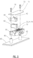
- FIG. 1-5 An exemplary embodiment of the connector arrangement 1, according to the present invention, is shown in Figures 1-5.
- a connector 20 is mounted to a printed circuit board (PCB) 10 by means of a bottom plate 80 having two guiding pins 60, 62 and two screws 70, 72.
- the connector 20 has two frame slots 30 and 32 to accommodate the respective guiding pins 60, 62 .
- the height of the pins 60 and 62 is slightly greater than the height of the connector 20, leaving a gap 36 between the PCB 10 and the connector 20.
- the outer diameter of the guiding pins 60, 62 and the inner diameters of the frame slots 30, 32 are designed to have a small gap therebetween to allow the connector 20 to move in the X-Y directions relative to the PCB 10.
- a vibration motor 40, encapsulated or surrounded by a rubber casing 50 (see Figure 4) is mechanically engaged with the connector 20, such that when the vibration motor 40 is activated, it causes the connector 20 to move in an oscillating manner, relative to the PCB
- Figure 2 is an exploded view of the connector arrangement of Figure 1.
- the vibration motor 40 has two electrodes 42 for providing electrical power to the vibration motor 40 for activating the motor 40 when desired.
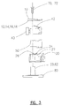
- a plurality of spring contacts 22, 24 and 26 extended from the connector 20 to make contact with the PCB 10.
- the spring contacts 22, 24 and 26 are clearly shown in Figure 3, which is an exploded view of connector arrangement, as viewed from one side thereof. Some or all of these spring contacts 22, 24 and 26 can be used to provide electrical connection between the connector 20 and the PCB 10, the others can be used as mechanical means for providing an urging force against the PCB 10 to keep the connector 20 away from the PCB 10.
- Figure 4 is another isometric view illustrating the top and rear sections of the connector arrangement without the PCB.
- the vibration motor 40 is separated from the connector 20 by the rubber casing 50 so as to avoid mechanical damages to the connector 20 due to the vibration.
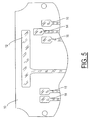
- One or some of these spring contacts can be used to make electrical contact to one or more electronically conductive pads on the bottom side of the PCB 10, as shown in Figure 5.
- FIG 5 is a bottom view of the PCB illustrating the electrically conductive pads on the PCB 10.
- two pads 18 are used to provide electrical connection to the electrodes 42 of the vibration motor 40 (see Figure 4);
- two pads 16 are used to provide electrical connection to the spring contacts 26 of the connectors;
- pad 14 is used to provide electrical connection to the spring contact 24; and
- a single pad 12 is used to provide electrical connection to the four spring contacts 22.
- the connector arrangement involves an electrical connector and a printed circuit board, wherein the electrical connection between the electrical connector and the printed circuit board is provided by one or more spring contacts and one or more electrically conducting pads.
- spring contacts and electrically conducting pads can also be used to provide electrical connection between a printed circuit board and a different electrical component, such as a switch, a solid-state display panel, and a keypad. Spring contacts and electrically conducting pads can be also used between two electrical components.
- the vibration motor is activated for causing the connector to move only when desired.
- a timer or a software program can be used to turn on the vibration motor periodically. It is also possible to use a monitoring means to check the electrical connection between the spring contacts and the electrically conducting pads, and the vibration motor is turned on only when needed.
- the spring contacts are caused to move by the vibration mechanism only within designed tolerances so the contact points between the spring contacts and the pad can be cleaned because of the mechanical stress or the rubbing action.
Landscapes
- Engineering & Computer Science (AREA)
- Metallurgy (AREA)
- Manufacturing & Machinery (AREA)
- Microelectronics & Electronic Packaging (AREA)
- Coupling Device And Connection With Printed Circuit (AREA)
- Details Of Connecting Devices For Male And Female Coupling (AREA)
- Manufacturing Of Electrical Connectors (AREA)
Abstract
Description
The connector arrangement comprises:
Claims (13)
- A method of improving electrical contact between a first electrical component and a second electrical component, wherein the first electrical component has at least one electrically conducting section, and the second electrical component has at least one spring contact for making electrical contact to the electrically conducting section, said method comprising the steps of:providing a vibration mechanism adjacent to the second electrical component; andproviding electrical power to the vibration mechanism for causing the second electrical component to move relative to the first electrical component, thereby causing the spring contact to rub against the electrically conducting section of the first electrical component.
- The method of claim 1, wherein the first electrical component comprises a circuit board.
- The method of claim 1, wherein the first electrical component comprises a printed circuit board.
- The method of claim 1, wherein the second electrical component comprises an electrical connector.
- The method of claim 1, wherein the electrical power is provided to the vibration mechanism when desired.
- The method of claim 1, wherein the electrical power is provided to the vibration mechanism when needed.
- The method of claim 1, wherein the vibration mechanism comprises a motor.
- A connector arrangement in an electronic device comprising a first electrical component having at least one electrically conducting section and a second electrical component having at least one spring contact for making electrical contact with the electrically conducting section of the first electrical component, said connector arrangement comprises:a vibration mechanism, located adjacent to the second electrical component, capable of causing the second electrical component to move relative to the circuit board, thereby causing the spring contact to rub against the electrically conducting section of the first electrical component; andmeans, electrically connected to the vibration mechanism, for providing electrical power to the vibration mechanism to cause the vibration mechanism to move the second electrical component when desired.
- The arrangement of claim 8, wherein the first electrical component comprises a circuit board.
- The arrangement of claim 8, wherein the first electrical component comprises a printed circuit board.
- The arrangement of claim 8, wherein the second electrical component comprises an electrical connector.
- The arrangement of claim 8, wherein the vibration mechanism comprises a motor.
- The arrangement of claim 8, further comprising a buffering means separating the vibration mechanism from the second electrical component for avoiding mechanical damage to the second electric component when the vibration mechanism moves the second electrical component.
Applications Claiming Priority (2)
| Application Number | Priority Date | Filing Date | Title |
|---|---|---|---|
| US09/782,674 US6347945B1 (en) | 2001-02-13 | 2001-02-13 | Method and device for improving electrical contact of spring connectors |
| US782674 | 2001-02-13 |
Publications (3)
| Publication Number | Publication Date |
|---|---|
| EP1231682A2 true EP1231682A2 (en) | 2002-08-14 |
| EP1231682A3 EP1231682A3 (en) | 2003-12-03 |
| EP1231682B1 EP1231682B1 (en) | 2005-11-09 |
Family
ID=25126821
Family Applications (1)
| Application Number | Title | Priority Date | Filing Date |
|---|---|---|---|
| EP02250517A Expired - Lifetime EP1231682B1 (en) | 2001-02-13 | 2002-01-25 | Method and device for improving electrical contact of spring connectors |
Country Status (5)
| Country | Link |
|---|---|
| US (1) | US6347945B1 (en) |
| EP (1) | EP1231682B1 (en) |
| JP (1) | JP2002246084A (en) |
| AT (1) | ATE309632T1 (en) |
| DE (1) | DE60207123T2 (en) |
Cited By (1)
| Publication number | Priority date | Publication date | Assignee | Title |
|---|---|---|---|---|
| US7310360B2 (en) | 2004-10-25 | 2007-12-18 | The Boeing Company | Apparatus and method for face cooling of optical components of a laser system |
Families Citing this family (2)
| Publication number | Priority date | Publication date | Assignee | Title |
|---|---|---|---|---|
| GB2404429B (en) * | 2003-07-31 | 2006-11-29 | Research In Motion Ltd | Vibration motor boot |
| US20140039693A1 (en) * | 2012-08-02 | 2014-02-06 | Honeywell Scanning & Mobility | Input/output connector contact cleaning |
Family Cites Families (4)
| Publication number | Priority date | Publication date | Assignee | Title |
|---|---|---|---|---|
| US6133657A (en) * | 1994-09-20 | 2000-10-17 | Motorola, Inc. | Vibrator bracket |
| JP3251305B2 (en) * | 1997-10-31 | 2002-01-28 | 三菱電機株式会社 | Vibrator mounting structure |
| US5975094A (en) * | 1997-11-26 | 1999-11-02 | Speedfam Corporation | Method and apparatus for enhanced cleaning of a workpiece with mechanical energy |
| US6254416B1 (en) * | 2000-05-18 | 2001-07-03 | Molex Incorporated | Vibrator motor holder |
-
2001
- 2001-02-13 US US09/782,674 patent/US6347945B1/en not_active Expired - Fee Related
- 2001-12-25 JP JP2001392014A patent/JP2002246084A/en active Pending
-
2002
- 2002-01-25 AT AT02250517T patent/ATE309632T1/en not_active IP Right Cessation
- 2002-01-25 DE DE60207123T patent/DE60207123T2/en not_active Expired - Lifetime
- 2002-01-25 EP EP02250517A patent/EP1231682B1/en not_active Expired - Lifetime
Cited By (1)
| Publication number | Priority date | Publication date | Assignee | Title |
|---|---|---|---|---|
| US7310360B2 (en) | 2004-10-25 | 2007-12-18 | The Boeing Company | Apparatus and method for face cooling of optical components of a laser system |
Also Published As
| Publication number | Publication date |
|---|---|
| EP1231682A3 (en) | 2003-12-03 |
| JP2002246084A (en) | 2002-08-30 |
| EP1231682B1 (en) | 2005-11-09 |
| DE60207123T2 (en) | 2007-02-22 |
| DE60207123D1 (en) | 2005-12-15 |
| US6347945B1 (en) | 2002-02-19 |
| ATE309632T1 (en) | 2005-11-15 |
Similar Documents
| Publication | Publication Date | Title |
|---|---|---|
| CN1095181C (en) | Rotary operation electronic components | |
| JP2005353563A (en) | Switch module for cellular phone | |
| KR20080014087A (en) | Connectors, circuit boards and electronics | |
| JP2001266700A (en) | Push switch | |
| KR20210016631A (en) | Connector for cable | |
| WO2001048872A1 (en) | Coaxial connector with switch | |
| US6347945B1 (en) | Method and device for improving electrical contact of spring connectors | |
| RU2006137292A (en) | DEVICE WITH ELECTRIC MOTOR AND MAIN PRINTED BOARD AND METHOD OF INSTALLATION | |
| JP2006521677A (en) | High density electrical connector | |
| JP2001244599A (en) | Ic mounting structure and position fixing sheet for bga type ic | |
| JPH1141682A (en) | Microphone mounting device and mounting method | |
| JP2004172128A (en) | Double contact electric compression connector | |
| TWI520449B (en) | Electric connector | |
| EP0984454A3 (en) | A connector for a hard disk drive | |
| CN1293584C (en) | Lever switch | |
| JPH1154174A (en) | Current-carrying connection structure | |
| JP2001035314A (en) | Switching device | |
| KR102420030B1 (en) | Connector for Flat Cable | |
| KR100989646B1 (en) | Automatic Main Distributing Frame Appratus | |
| KR940012754A (en) | Brush plate equipment for electromechanical machines | |
| JPH065171U (en) | connector | |
| JP3331467B2 (en) | ZIF connector device | |
| KR100739934B1 (en) | Connector | |
| JP2004208432A (en) | Electrical connection structure between vibrator and circuit board and portable terminal device | |
| JP2001095200A (en) | Electronics |
Legal Events
| Date | Code | Title | Description |
|---|---|---|---|
| PUAI | Public reference made under article 153(3) epc to a published international application that has entered the european phase |
Free format text: ORIGINAL CODE: 0009012 |
|
| AK | Designated contracting states |
Kind code of ref document: A2 Designated state(s): AT BE CH CY DE DK ES FI FR GB GR IE IT LI LU MC NL PT SE TR |
|
| AX | Request for extension of the european patent |
Free format text: AL;LT;LV;MK;RO;SI |
|
| PUAL | Search report despatched |
Free format text: ORIGINAL CODE: 0009013 |
|
| AK | Designated contracting states |
Kind code of ref document: A3 Designated state(s): AT BE CH CY DE DK ES FI FR GB GR IE IT LI LU MC NL PT SE TR |
|
| AX | Request for extension of the european patent |
Extension state: AL LT LV MK RO SI |
|
| 17P | Request for examination filed |
Effective date: 20040318 |
|
| 17Q | First examination report despatched |
Effective date: 20040504 |
|
| AKX | Designation fees paid |
Designated state(s): AT BE CH CY DE DK ES FI FR GB GR IE IT LI LU MC NL PT SE TR |
|
| GRAP | Despatch of communication of intention to grant a patent |
Free format text: ORIGINAL CODE: EPIDOSNIGR1 |
|
| GRAS | Grant fee paid |
Free format text: ORIGINAL CODE: EPIDOSNIGR3 |
|
| GRAA | (expected) grant |
Free format text: ORIGINAL CODE: 0009210 |
|
| TCNL | Nl: translation of patent claims filed | ||
| AK | Designated contracting states |
Kind code of ref document: B1 Designated state(s): AT BE CH CY DE DK ES FI FR GB GR IE IT LI LU MC NL PT SE TR |
|
| PG25 | Lapsed in a contracting state [announced via postgrant information from national office to epo] |
Ref country code: IT Free format text: LAPSE BECAUSE OF FAILURE TO SUBMIT A TRANSLATION OF THE DESCRIPTION OR TO PAY THE FEE WITHIN THE PRESCRIBED TIME-LIMIT;WARNING: LAPSES OF ITALIAN PATENTS WITH EFFECTIVE DATE BEFORE 2007 MAY HAVE OCCURRED AT ANY TIME BEFORE 2007. THE CORRECT EFFECTIVE DATE MAY BE DIFFERENT FROM THE ONE RECORDED. Effective date: 20051109 Ref country code: CH Free format text: LAPSE BECAUSE OF FAILURE TO SUBMIT A TRANSLATION OF THE DESCRIPTION OR TO PAY THE FEE WITHIN THE PRESCRIBED TIME-LIMIT Effective date: 20051109 Ref country code: BE Free format text: LAPSE BECAUSE OF FAILURE TO SUBMIT A TRANSLATION OF THE DESCRIPTION OR TO PAY THE FEE WITHIN THE PRESCRIBED TIME-LIMIT Effective date: 20051109 Ref country code: LI Free format text: LAPSE BECAUSE OF FAILURE TO SUBMIT A TRANSLATION OF THE DESCRIPTION OR TO PAY THE FEE WITHIN THE PRESCRIBED TIME-LIMIT Effective date: 20051109 Ref country code: AT Free format text: LAPSE BECAUSE OF FAILURE TO SUBMIT A TRANSLATION OF THE DESCRIPTION OR TO PAY THE FEE WITHIN THE PRESCRIBED TIME-LIMIT Effective date: 20051109 Ref country code: FI Free format text: LAPSE BECAUSE OF FAILURE TO SUBMIT A TRANSLATION OF THE DESCRIPTION OR TO PAY THE FEE WITHIN THE PRESCRIBED TIME-LIMIT Effective date: 20051109 |
|
| REG | Reference to a national code |
Ref country code: GB Ref legal event code: FG4D |
|
| REG | Reference to a national code |
Ref country code: CH Ref legal event code: EP |
|
| REG | Reference to a national code |
Ref country code: IE Ref legal event code: FG4D |
|
| REF | Corresponds to: |
Ref document number: 60207123 Country of ref document: DE Date of ref document: 20051215 Kind code of ref document: P |
|
| PG25 | Lapsed in a contracting state [announced via postgrant information from national office to epo] |
Ref country code: IE Free format text: LAPSE BECAUSE OF NON-PAYMENT OF DUE FEES Effective date: 20060125 |
|
| PG25 | Lapsed in a contracting state [announced via postgrant information from national office to epo] |
Ref country code: MC Free format text: LAPSE BECAUSE OF NON-PAYMENT OF DUE FEES Effective date: 20060131 Ref country code: LU Free format text: LAPSE BECAUSE OF NON-PAYMENT OF DUE FEES Effective date: 20060131 |
|
| PG25 | Lapsed in a contracting state [announced via postgrant information from national office to epo] |
Ref country code: SE Free format text: LAPSE BECAUSE OF FAILURE TO SUBMIT A TRANSLATION OF THE DESCRIPTION OR TO PAY THE FEE WITHIN THE PRESCRIBED TIME-LIMIT Effective date: 20060209 Ref country code: DK Free format text: LAPSE BECAUSE OF FAILURE TO SUBMIT A TRANSLATION OF THE DESCRIPTION OR TO PAY THE FEE WITHIN THE PRESCRIBED TIME-LIMIT Effective date: 20060209 Ref country code: GR Free format text: LAPSE BECAUSE OF FAILURE TO SUBMIT A TRANSLATION OF THE DESCRIPTION OR TO PAY THE FEE WITHIN THE PRESCRIBED TIME-LIMIT Effective date: 20060209 |
|
| PG25 | Lapsed in a contracting state [announced via postgrant information from national office to epo] |
Ref country code: ES Free format text: LAPSE BECAUSE OF FAILURE TO SUBMIT A TRANSLATION OF THE DESCRIPTION OR TO PAY THE FEE WITHIN THE PRESCRIBED TIME-LIMIT Effective date: 20060220 |
|
| PG25 | Lapsed in a contracting state [announced via postgrant information from national office to epo] |
Ref country code: PT Free format text: LAPSE BECAUSE OF FAILURE TO SUBMIT A TRANSLATION OF THE DESCRIPTION OR TO PAY THE FEE WITHIN THE PRESCRIBED TIME-LIMIT Effective date: 20060410 |
|
| ET | Fr: translation filed | ||
| REG | Reference to a national code |
Ref country code: CH Ref legal event code: PL |
|
| PLBE | No opposition filed within time limit |
Free format text: ORIGINAL CODE: 0009261 |
|
| STAA | Information on the status of an ep patent application or granted ep patent |
Free format text: STATUS: NO OPPOSITION FILED WITHIN TIME LIMIT |
|
| 26N | No opposition filed |
Effective date: 20060810 |
|
| REG | Reference to a national code |
Ref country code: IE Ref legal event code: MM4A |
|
| PG25 | Lapsed in a contracting state [announced via postgrant information from national office to epo] |
Ref country code: TR Free format text: LAPSE BECAUSE OF FAILURE TO SUBMIT A TRANSLATION OF THE DESCRIPTION OR TO PAY THE FEE WITHIN THE PRESCRIBED TIME-LIMIT Effective date: 20051109 |
|
| PG25 | Lapsed in a contracting state [announced via postgrant information from national office to epo] |
Ref country code: CY Free format text: LAPSE BECAUSE OF FAILURE TO SUBMIT A TRANSLATION OF THE DESCRIPTION OR TO PAY THE FEE WITHIN THE PRESCRIBED TIME-LIMIT Effective date: 20051109 |
|
| PGFP | Annual fee paid to national office [announced via postgrant information from national office to epo] |
Ref country code: FR Payment date: 20120202 Year of fee payment: 11 |
|
| PGFP | Annual fee paid to national office [announced via postgrant information from national office to epo] |
Ref country code: DE Payment date: 20120118 Year of fee payment: 11 |
|
| PGFP | Annual fee paid to national office [announced via postgrant information from national office to epo] |
Ref country code: GB Payment date: 20120125 Year of fee payment: 11 |
|
| PGFP | Annual fee paid to national office [announced via postgrant information from national office to epo] |
Ref country code: NL Payment date: 20120117 Year of fee payment: 11 |
|
| REG | Reference to a national code |
Ref country code: NL Ref legal event code: V1 Effective date: 20130801 |
|
| GBPC | Gb: european patent ceased through non-payment of renewal fee |
Effective date: 20130125 |
|
| REG | Reference to a national code |
Ref country code: FR Ref legal event code: ST Effective date: 20130930 |
|
| PG25 | Lapsed in a contracting state [announced via postgrant information from national office to epo] |
Ref country code: NL Free format text: LAPSE BECAUSE OF NON-PAYMENT OF DUE FEES Effective date: 20130801 Ref country code: DE Free format text: LAPSE BECAUSE OF NON-PAYMENT OF DUE FEES Effective date: 20130801 |
|
| REG | Reference to a national code |
Ref country code: DE Ref legal event code: R119 Ref document number: 60207123 Country of ref document: DE Effective date: 20130801 |
|
| PG25 | Lapsed in a contracting state [announced via postgrant information from national office to epo] |
Ref country code: GB Free format text: LAPSE BECAUSE OF NON-PAYMENT OF DUE FEES Effective date: 20130125 Ref country code: FR Free format text: LAPSE BECAUSE OF NON-PAYMENT OF DUE FEES Effective date: 20130131 |