EP1231631A2 - MFMOS/MFMS non-volatile memory transistors and method of making same - Google Patents
MFMOS/MFMS non-volatile memory transistors and method of making same Download PDFInfo
- Publication number
- EP1231631A2 EP1231631A2 EP02250984A EP02250984A EP1231631A2 EP 1231631 A2 EP1231631 A2 EP 1231631A2 EP 02250984 A EP02250984 A EP 02250984A EP 02250984 A EP02250984 A EP 02250984A EP 1231631 A2 EP1231631 A2 EP 1231631A2
- Authority
- EP
- European Patent Office
- Prior art keywords
- electrode
- layer
- region
- ferroelectric
- memory transistor
- Prior art date
- Legal status (The legal status is an assumption and is not a legal conclusion. Google has not performed a legal analysis and makes no representation as to the accuracy of the status listed.)
- Withdrawn
Links
Images


Classifications
-
- H—ELECTRICITY
- H10—SEMICONDUCTOR DEVICES; ELECTRIC SOLID-STATE DEVICES NOT OTHERWISE PROVIDED FOR
- H10D—INORGANIC ELECTRIC SEMICONDUCTOR DEVICES
- H10D84/00—Integrated devices formed in or on semiconductor substrates that comprise only semiconducting layers, e.g. on Si wafers or on GaAs-on-Si wafers
- H10D84/80—Integrated devices formed in or on semiconductor substrates that comprise only semiconducting layers, e.g. on Si wafers or on GaAs-on-Si wafers characterised by the integration of at least one component covered by groups H10D12/00 or H10D30/00, e.g. integration of IGFETs
-
- H—ELECTRICITY
- H10—SEMICONDUCTOR DEVICES; ELECTRIC SOLID-STATE DEVICES NOT OTHERWISE PROVIDED FOR
- H10D—INORGANIC ELECTRIC SEMICONDUCTOR DEVICES
- H10D64/00—Electrodes of devices having potential barriers
- H10D64/01—Manufacture or treatment
- H10D64/031—Manufacture or treatment of data-storage electrodes
- H10D64/033—Manufacture or treatment of data-storage electrodes comprising ferroelectric layers
-
- H—ELECTRICITY
- H10—SEMICONDUCTOR DEVICES; ELECTRIC SOLID-STATE DEVICES NOT OTHERWISE PROVIDED FOR
- H10D—INORGANIC ELECTRIC SEMICONDUCTOR DEVICES
- H10D30/00—Field-effect transistors [FET]
- H10D30/01—Manufacture or treatment
- H10D30/021—Manufacture or treatment of FETs having insulated gates [IGFET]
- H10D30/0415—Manufacture or treatment of FETs having insulated gates [IGFET] of FETs having ferroelectric gate insulators
-
- H—ELECTRICITY
- H10—SEMICONDUCTOR DEVICES; ELECTRIC SOLID-STATE DEVICES NOT OTHERWISE PROVIDED FOR
- H10D—INORGANIC ELECTRIC SEMICONDUCTOR DEVICES
- H10D30/00—Field-effect transistors [FET]
- H10D30/60—Insulated-gate field-effect transistors [IGFET]
- H10D30/701—IGFETs having ferroelectric gate insulators, e.g. ferroelectric FETs
Definitions
- This invention relates to ferroelectric non-volatile integrated circuits, and specifically to a simplified fabrication technique which minimizes etching-induced ferroelectric stack damage.
- a gate stack of a state-of-the-art ferroelectric (FE) memory transistor includes formation of a self-aligned FE stack, which includes deposition and etching of a top electrode material, the ferroelectric material, and a bottom electrode material.
- a self-aligned FE stack which includes deposition and etching of a top electrode material, the ferroelectric material, and a bottom electrode material.
- a method of fabricating a non-volatile ferroelectric memory transistor includes a) preparing a silicon substrate, including forming an active region on the substrate; b) implanting ions to form a source region and a drain region in the active region; c) forming a bottom electrode; d) depositing a ferroelectric layer over the active region; e) depositing a top electrode; f) depositing an insulating oxide layer over the active region; and g) metallizing a structure obtained by the above-described steps a) to f) to form a source electrode, a gate electrode and a drain electrode.
- a non-volatile ferroelectric memory transistor includes a silicon substrate having an active region formed thereon; a source region and a drain region formed about a gate region in the active region; a bottom electrode formed above the gate region, wherein the bottom electrode has a predetermined area within a peripheral boundary; a ferroelectric layer extending over and beyond the bottom electrode peripheral boundary; a top electrode formed on the ferroelectric layer; an insulating oxide layer; and a source electrode, a gate electrode and a drain electrode.
- An object of the invention is to fabricate a ferroelectric non-volatile memory transistor which does not require gate stack etching.
- a further object of the invention is to fabricate a ferroelectric non-volatile memory transistor with minimal etching-induced damage.
- Another object of the invention is to provide a fabrication process for a ferroelectric non-volatile memory transistor which is less complex than prior art techniques.
- the ferroelectric memory transistor of the invention may be formed on a silicon-on-insulator (SOI) substrate, such as Separation by IMplantation of Oxygen (SIMOX), or, it may be formed in a bulk silicon substrate.
- SOI silicon-on-insulator
- SIMOX Separation by IMplantation of Oxygen
- silicon substrate refers to either a SOI substrate or to a bulk silicon substrate.
- the method of the invention overcomes the problems associated with etching to form a self-aligned ferroelectric (FE) gate stack, and to also overcome the problems associated with etching-induced damage.
- the fabrication method of the invention for a FE non-volatile memory transistor does not require etching of the FE material of the gate stack. Further, the top electrode and the bottom electrode do not need to be self-aligned.
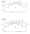
- a substrate 10 As previously noted, this may be a bulk or SOI substrate. State-of-the-art processes are followed for device isolation, with shallow trench isolation (STI) being used as the preferred technique for device isolation resulting in the formation of oxide areas 11. Implantation of Boron ions, at a dose of about 1 ⁇ 10 12 cm -2 to 5 ⁇ 10 13 cm -2 , and at an energy level of 30 keV to 60 keV results in the formation of p-well 12, forming an active region on substrate 10. A gate region is oxidized, resulting in a gate oxide 14, when fabricating a metal-ferro-metal oxide semiconductor (MFMOS) transistor.
- MMOS metal-ferro-metal oxide semiconductor
- a surface channel is formed when fabricating a metal-ferro-metal semiconductor (MFMS) transistor.
- a bottom electrode 16 is deposited by CVD.
- Bottom electrode 16 is preferably formed of Iridium, deposited to a thickness of between about 100 nm and 200 nm.
- a layer of photoresist is applied to the desired areas, and bottom electrode 16 is etched, leaving sufficient bottom electrode material to cover a gate region.
- Bottom electrode 16 has a predetermined area located within a peripheral boundary.
- Arsenic ions are implanted at a dose of about 1 ⁇ 10 15 cm -2 to 3 ⁇ 10 15 cm -2 , and at an energy level of 20 keV to 40 keV, to form a source region 18 and a drain region 20, which are located about a gate region, resulting in the structure depicted in Fig. 1.
- An oxide layer 22 is formed by chemical vapor deposition (CVD) to a thickness of between about 200 nm and 400 nm, which is thicker than that of bottom electrode 16. Oxide layer 22 is thinned by chemical-mechanical polishing (CMP) to the upper surface of bottom electrode 16, exposing the bottom electrode, as shown in Fig. 2.
- CVD chemical vapor deposition
- CMP chemical-mechanical polishing
- a FE layer 24 is formed by CVD to a thickness of between about 100 nm and 400 nm.
- the FE material may be any of the following: Pb(Zr, Ti)O 3 (PZT), SrBi 2 Ta 2 O 9 (SBT), Pb 5 Ge 3 O 11 , BaTiO 3 , or LiNbO 3 .
- a top electrode 26, preferably formed of Platinum, is deposited by CVD to a thickness of between about 100 nm and 300 nm.
- the top electrode 26 may be deposited by sputtering. Photoresist is applied to specific regions of the structure, and the top electrode is etched, resulting in the structure shown in Fig. 3.
- the selectivity of etching of top electrode 26 vs. FE layer 24 is not critical.
- a barrier insulation layer 28 is deposited by CVD.
- a material such as TiO 2 is suitable for this layer, if required, and may be deposited to a thickness of between about 10 nm and 30.
- Barrier insulation layer 28 is provided to stop the diffusion of H 2 into the FE layer during annealing.
- An oxide layer 30 is next deposited by CVD. Photoresist is applied prior to etching of contact holes in the insulating oxide. The structure is then metallized, and then etched, forming source electrode 32, gate electrode 34, and drain electrode 36, resulting in the final MFMOS memory transistor structure shown at 38 in Fig. 5.
- a surface channel n-layer 42 is formed in place of gate oxide layer 14 in Figs. 1-5.
- Surface channel 42 is formed by implantation of Arsenic ions, at a dose of about 1 ⁇ 10 11 cm -2 to 5 ⁇ 10 12 cm -2 , and at an energy level of about 15 keV to 30 keV, resulting in a n-layer between p-well 12 and bottom electrode 16.
- top electrode 26 and bottom electrode 16 are not self-aligned.
- the effective remnant charge is reduced by A OVERLAP /A BOT , where A OVERLAP is the area of overlap between top electrode 26 and bottom electrode 16, and A BOT is the area of bottom electrode 16.
- the top electrode When the top electrode is larger than the bottom electrode, the bottom electrode is generally completely covered by the top electrode, and the effective remnant charge is the same as that of a self-aligned gate stack of the same size electrodes.
- the top electrode may also cover portions of source region 18 and/or drain region 20, and the charge on the FE material will induce a charge on the source/drain junction. This induced charge makes the source region and/or drain region more conductive when the memory cell is programmed to a high conductive state, and less conductive when the memory cell is programmed to a low conductive state. Thus, this form of overlap does not produce any undesirable effects.
- the contact via is located a short distance laterally away from bottom electrode 16, and, because the etched area is relatively small, any plasma etching damage is minimal.
- the method of the invention eliminates the need to etch the FE layer for a self-aligning process. The only etching which occurs to the FE layers is the formation of via holes, which is quite minimal, and not likely to result in any loss of non-volatile properties in the FE layer.
Landscapes
- Semiconductor Memories (AREA)
- Non-Volatile Memory (AREA)
Abstract
Description
Claims (28)
- A method of fabricating a non-volatile ferroelectric memory transistor, comprising:a) preparing a silicon substrate, including forming an active region on the substrate;b) implanting ions to form a source region and a drain region in the active region;c) forming a bottom electrode;d) depositing a ferroelectric layer over the active region;e) depositing a top electrode;f) depositing an insulating oxide layer over the active region; andg) metallizing a structure obtained by the steps a) to f) to form a source electrode, a gate electrode and a drain electrode.
- The method of claim 1 wherein said a) preparing includes forming a gate oxide layer in a gate region.
- The method of claim 1 wherein said a) preparing includes forming a surface channel in a gate region.
- The method of claim 3 wherein said forming a surface channel region includes forming an n-region by implantation of Arsenic ions, at a dose of about 1·1011 cm-2 to 5·1012 cm-2, and at an energy level of 15 keV to 30 keV.
- The method of claim 1 wherein said c) forming a bottom electrode includes chemical vapor deposition of a layer of Iridium, deposited to a thickness of between about 100 nm and 200 nm, and which further includes etching the Iridium layer to form a bottom electrode of a predetermined area.
- The method of claim 5 which further includes chemical vapor deposition of oxide layer to a thickness of between about 200 nm and 400 nm, and thinning the oxide layer by chemical mechanical polishing to the upper surface of bottom electrode, thereby exposing the upper surface of the bottom electrode.
- The method of claim 1 wherein said b) implanting ions includes implanting Arsenic ions at a dose of about 1·1015 cm-2 to 3·1015 cm2, and at an energy level of 20 keV to 40 keV.
- The method of claim 1 wherein said d) depositing a ferroelectric layer includes depositing a ferroelectric material by chemical vapor deposition to a thickness of between about 100 nm and 400 nm.
- The method of claim 8 wherein said depositing includes depositing a ferroelectric material taken from the group of ferroelectric materials consisting of Pb(Zr, Ti)O3 (PZT), SrBi2Ta2O9 (SBT), Pb5Ge3O11, BaTiO3, and LiNbO3.
- The method of claim 1 wherein said e) depositing a top electrode includes depositing a layer of Platinum, by a deposition process taken from the group of processes consisting of chemical vapor deposition and sputtering to a thickness of between about 100 nm and 300 nm, masking the desired area of the top electrode, and etching the unmasked material.
- The method of claim 10 wherein said e) depositing a top electrode includes forming a top electrode having an area greater than the area of the bottom electrode.
- The method of claim 10 wherein said e) depositing a top electrode includes forming a top electrode having an area which overlaps the source region and the drain region.
- The method of claim 1 which further includes forming a barrier insulation layer which extends over the ferroelectric layer and the top electrode.
- The method of claim 13 wherein said forming a barrier insulation layer includes depositing a layer of TiO2 to a thickness of between about 10 nm and 30 nm.
- A non-volatile ferroelectric memory transistor comprising:a silicon substrate having an active region formed thereon;a source region and a drain region formed about a gate region in said active region;a bottom electrode formed above said gate region, wherein said bottom electrode has a predetermined area within a peripheral boundary;
a ferroelectric layer extending over and beyond the bottom electrode peripheral boundary;a top electrode formed on said ferroelectric layer;an insulating oxide layer; anda source electrode, a gate electrode and a drain electrode. - The non-volatile ferroelectric memory transistor of claim 15 which further includes a barrier insulation layer extending over said ferroelectric layer and said top electrode.
- The non-volatile ferroelectric memory transistor of claim 16 wherein said barrier insulation layer includes a layer of TiO2 deposited to a thickness of between about 10 nm and 30 nm.
- The non-volatile ferroelectric memory transistor of claim 15 wherein said top electrode has a surface area greater than said bottom electrode predetermined area.
- The non-volatile ferroelectric memory transistor of claim 15 wherein said top electrode extends at least partially over said source region and said drain region.
- The non-volatile ferroelectric memory transistor of claim 15 which further includes a gate oxide layer formed on said silicon substrate.
- The non-volatile ferroelectric memory transistor of claim 15 which further includes a surface channel layer formed on said silicon substrate.
- The non-volatile ferroelectric memory transistor of claim 15 wherein said bottom electrode is formed of Iridium to a thickness of between about 100 nm and 200 nm.
- The non-volatile ferroelectric memory transistor of claim 15 wherein said ferroelectric layer is formed of a ferroelectric material taken from the group of ferroelectric materials consisting of Pb(Zr, Ti)O3 (PZT), SrBi2Ta2O9 (SBT), Pb5Ge3O11, BaTiO3, and LiNbO3, and which is deposited to a thickness of between about 100 nm and 400 nm.
- The non-volatile ferroelectric memory transistor of claim 15 wherein said top electrode is formed of Platinum to a thickness of between about 100 nm and 300 nm.
- A method of fabricating a non-volatile ferroelectric memory transistor including source and drain regions in an active region of a semiconductor substrate, a gate region between the source and drain regions, a bottom electrode formed on the gate region, top electrode and a ferroelectric layer between the bottom and top electrodes, wherein the top and bottom electrodes are formed using separate non self-aligned etching steps, with no etching of the ferroelectric layer.
- A method according to claim 25 wherein the top electrode is formed with an area which is greater than that of the bottom electrode.
- A method according to claim 26 wherein the top electrode is formed so as to project at least partially over the source and/or drain region.
- A method according to any of claims 25 to 27, including the further step of metallizing to form source gate and drain electrodes, the source and drain electrodes extending depthwise of the structure to the source and drain regions, respectively, and penetrating through the unetched ferroelectric layer.
Applications Claiming Priority (2)
| Application Number | Priority Date | Filing Date | Title |
|---|---|---|---|
| US783815 | 2001-02-13 | ||
| US09/783,815 US20020109166A1 (en) | 2001-02-13 | 2001-02-13 | MFMOS/MFMS non-volatile memory transistors and method of making same |
Publications (2)
| Publication Number | Publication Date |
|---|---|
| EP1231631A2 true EP1231631A2 (en) | 2002-08-14 |
| EP1231631A3 EP1231631A3 (en) | 2004-12-29 |
Family
ID=25130471
Family Applications (1)
| Application Number | Title | Priority Date | Filing Date |
|---|---|---|---|
| EP02250984A Withdrawn EP1231631A3 (en) | 2001-02-13 | 2002-02-13 | MFMOS/MFMS non-volatile memory transistors and method of making same |
Country Status (4)
| Country | Link |
|---|---|
| US (2) | US20020109166A1 (en) |
| EP (1) | EP1231631A3 (en) |
| JP (1) | JP3907100B2 (en) |
| KR (1) | KR20020066997A (en) |
Families Citing this family (5)
| Publication number | Priority date | Publication date | Assignee | Title |
|---|---|---|---|---|
| JP4887566B2 (en) * | 2001-03-27 | 2012-02-29 | 独立行政法人産業技術総合研究所 | Semiconductor non-volatile memory element and manufacturing method thereof |
| US6838995B2 (en) | 2002-04-24 | 2005-01-04 | The United States Of America As Represented By The Administrator Of The National Aeronautics And Space Administration | Method for anticipating problems with electrical wiring |
| US6985083B2 (en) * | 2002-04-24 | 2006-01-10 | The United States Of America As Represented By The Administrator Of The National Aeronautics And Space Administration | Marking electrical wiring with condition indicators |
| JP7038559B2 (en) * | 2018-02-05 | 2022-03-18 | ルネサスエレクトロニクス株式会社 | Manufacturing method of semiconductor device |
| US11063065B2 (en) * | 2018-07-06 | 2021-07-13 | Samsung Electronics Co., Ltd. | Semiconductor device having a negative capacitance using ferroelectrical material |
Family Cites Families (6)
| Publication number | Priority date | Publication date | Assignee | Title |
|---|---|---|---|---|
| US5384729A (en) * | 1991-10-28 | 1995-01-24 | Rohm Co., Ltd. | Semiconductor storage device having ferroelectric film |
| JP3281839B2 (en) * | 1997-06-16 | 2002-05-13 | 三洋電機株式会社 | Dielectric memory and method of manufacturing the same |
| US5907762A (en) * | 1997-12-04 | 1999-05-25 | Sharp Microelectronics Technology, Inc. | Method of manufacture of single transistor ferroelectric memory cell using chemical-mechanical polishing |
| US6011285A (en) * | 1998-01-02 | 2000-01-04 | Sharp Laboratories Of America, Inc. | C-axis oriented thin film ferroelectric transistor memory cell and method of making the same |
| US6048740A (en) * | 1998-11-05 | 2000-04-11 | Sharp Laboratories Of America, Inc. | Ferroelectric nonvolatile transistor and method of making same |
| US6303502B1 (en) * | 2000-06-06 | 2001-10-16 | Sharp Laboratories Of America, Inc. | MOCVD metal oxide for one transistor memory |
-
2001
- 2001-02-13 US US09/783,815 patent/US20020109166A1/en not_active Abandoned
-
2002
- 2002-01-30 JP JP2002022530A patent/JP3907100B2/en not_active Expired - Fee Related
- 2002-02-08 KR KR1020020007479A patent/KR20020066997A/en not_active Ceased
- 2002-02-13 EP EP02250984A patent/EP1231631A3/en not_active Withdrawn
-
2003
- 2003-03-24 US US10/395,368 patent/US6762063B2/en not_active Expired - Lifetime
Also Published As
| Publication number | Publication date |
|---|---|
| JP2002246570A (en) | 2002-08-30 |
| EP1231631A3 (en) | 2004-12-29 |
| JP3907100B2 (en) | 2007-04-18 |
| US20030173600A1 (en) | 2003-09-18 |
| KR20020066997A (en) | 2002-08-21 |
| US20020109166A1 (en) | 2002-08-15 |
| US6762063B2 (en) | 2004-07-13 |
Similar Documents
| Publication | Publication Date | Title |
|---|---|---|
| EP0999597B1 (en) | Ferroelectric nonvolatile transistor and method of making same | |
| US6200866B1 (en) | Use of silicon germanium and other alloys as the replacement gate for the fabrication of MOSFET | |
| US7659171B2 (en) | Methods and structure for forming self-aligned borderless contacts for strain engineered logic devices | |
| JP2005514771A (en) | Body-coupled silicon semiconductor device on insulating film and method thereof | |
| JP2002324905A (en) | Method of forming integrated circuit having body contact | |
| US6531325B1 (en) | Memory transistor and method of fabricating same | |
| US6905919B2 (en) | Method of forming a partially depleted silicon on insulator (PDSOI) transistor with a pad lock body extension | |
| US6566148B2 (en) | Method of making a ferroelectric memory transistor | |
| US6300172B1 (en) | Method of field isolation in silicon-on-insulator technology | |
| US7692243B2 (en) | Semiconductor device and method of manufacturing the same | |
| KR100470499B1 (en) | Method of making a self-aligned ferroelectric memory transistor | |
| US6858514B2 (en) | Low power flash memory cell and method | |
| US6762063B2 (en) | Method of fabricating non-volatile ferroelectric transistors | |
| KR100233802B1 (en) | Semiconductor device and manufacturing method thereof | |
| US5518949A (en) | Electrical isolation method for devices made on SOI wafer | |
| JP2003142694A (en) | Element isolation method for SOI device | |
| JP3411370B2 (en) | Semiconductor device manufacturing method and semiconductor device | |
| KR100511898B1 (en) | method of manufacturing semiconductor device | |
| US20020076888A1 (en) | Method for manufacturing semiconductor device | |
| JP2002118261A (en) | Semiconductor device and its fabricating method | |
| JP2000236030A (en) | Nonvolatile semiconductor memory device and method of manufacturing the same | |
| JPH04165668A (en) | Manufacture of semiconductor device | |
| JPH06268058A (en) | Semiconductor integrated circuit device |
Legal Events
| Date | Code | Title | Description |
|---|---|---|---|
| PUAI | Public reference made under article 153(3) epc to a published international application that has entered the european phase |
Free format text: ORIGINAL CODE: 0009012 |
|
| AK | Designated contracting states |
Kind code of ref document: A2 Designated state(s): AT BE CH CY DE DK ES FI FR GB GR IE IT LI LU MC NL PT SE TR |
|
| AX | Request for extension of the european patent |
Free format text: AL;LT;LV;MK;RO;SI |
|
| PUAL | Search report despatched |
Free format text: ORIGINAL CODE: 0009013 |
|
| AK | Designated contracting states |
Kind code of ref document: A3 Designated state(s): AT BE CH CY DE DK ES FI FR GB GR IE IT LI LU MC NL PT SE TR |
|
| AX | Request for extension of the european patent |
Extension state: AL LT LV MK RO SI |
|
| RIC1 | Information provided on ipc code assigned before grant |
Ipc: 7H 01L 21/28 B Ipc: 7H 01L 29/78 B Ipc: 7H 01L 21/336 A |
|
| 17P | Request for examination filed |
Effective date: 20050623 |
|
| AKX | Designation fees paid |
Designated state(s): DE FR GB |
|
| 17Q | First examination report despatched |
Effective date: 20071114 |
|
| STAA | Information on the status of an ep patent application or granted ep patent |
Free format text: STATUS: THE APPLICATION IS DEEMED TO BE WITHDRAWN |
|
| 18D | Application deemed to be withdrawn |
Effective date: 20080527 |