EP1231542A2 - Data transmission system - Google Patents
Data transmission system Download PDFInfo
- Publication number
- EP1231542A2 EP1231542A2 EP02250271A EP02250271A EP1231542A2 EP 1231542 A2 EP1231542 A2 EP 1231542A2 EP 02250271 A EP02250271 A EP 02250271A EP 02250271 A EP02250271 A EP 02250271A EP 1231542 A2 EP1231542 A2 EP 1231542A2
- Authority
- EP
- European Patent Office
- Prior art keywords
- clock signal
- data transmission
- data
- storage device
- memory
- Prior art date
- Legal status (The legal status is an assumption and is not a legal conclusion. Google has not performed a legal analysis and makes no representation as to the accuracy of the status listed.)
- Withdrawn
Links
Images



Classifications
-
- G—PHYSICS
- G06—COMPUTING OR CALCULATING; COUNTING
- G06F—ELECTRIC DIGITAL DATA PROCESSING
- G06F13/00—Interconnection of, or transfer of information or other signals between, memories, input/output devices or central processing units
- G06F13/38—Information transfer, e.g. on bus
- G06F13/382—Information transfer, e.g. on bus using universal interface adapter
- G06F13/385—Information transfer, e.g. on bus using universal interface adapter for adaptation of a particular data processing system to different peripheral devices
Definitions
- the invention relates to a data transmission system and, in particular, to a data transmission system which transmits data between a hard disk drive and a memory via an IDE interface.
- a data transmission system for example, a system which transmits data between a hard disk drive and a memory
- the data transmission system uses (diverts) an IP (Intellectual property) core and sometimes performs data transmission process at a speed higher than the maximum transmission rate of the IP core.
- IP Internet Protocol
- the data transmission system often uses one of three typical data transmission methods. That is, a PIO (Programmed I/O) transmission method, a multi-word DMA (Direct Memory Access) transmission method, and an UltraDMA transmission method.
- PIO Programmed I/O
- DMA Direct Memory Access
- UltraDMA UltraDMA
- the UltraDMA transmission method provides a high speed data transmission as described later, in recent years, most hard disks incorporated in personal computers adopts the UltraDMA transmission method. As a result, the UltraDMA transmission method has become a defacto standard.
- embodiments of the invention provide a data transmission system which is capable of performing a high speed data transmission process between a device (a storage device) and a memory without change of the frequency of a system clock.
- a data transmission system comprising a data transmission device which transmits data stored in a memory or an instruction command generated by a CPU to a storage device, and a clock generator which generates a first clock signal and a second clock signal which has a frequency lower than that of the first clock signal.
- the data transmission device transmits the instruction command from the CPU to the storage device by using the second clock signal, and after that, transmits the data from the memory to the storage device by using the first clock signal.
- the data transmission system is configured to have the data transmission device which transmits the data transmitted to and stored in the storage device, to the memory by using the first clock signal.
- the data transmission system is configured to have a hard disk drive as the storage device.
- the data transmission system is configured to have the data transmission device which comprises an interface transmitting the data to the storage device by using the first clock signal, and transmitting the instruction command to the storage device by using the second clock signal.
- the data transmission system is configured to have the storage device including a status register, and the first clock signal is used on accessing the status register.
- the data transmission system is configured to have the interface which changes a clock signal from the first clock signal to the second clock signal, or from the second clock signal to the first signal, based on a signal supplied in response to a notification that the storage device successfully receives the data or the instruction command.
- a method of transmitting data in a data transmission system having a data transmission device which transmits data stored in a memory or an instruction command generated by a CPU to a storage device comprises the steps of (1) generating, at a clock generator, a first clock signal, and a second clock signal which has a frequency lower than that of the first clock signal, (2) transmitting, at the data transmission device, the instruction command from the CPU to the storage device by using the second clock signal, and (3) transmitting, at the data transmission device, the data from the memory to the storage device by using the first clock signal.
- a recording medium readable by a computer, tangibly embodying a program of instructions executable by the computer to perform a method of transmitting data in a data transmission system having a data transmission device which transmits data stored in a memory or an instruction command generated by a CPU to a storage device.
- the method comprises the steps of (1) generating, at a clock generator, a first clock signal, and a second clock signal which has a frequency lower than that of the first clock signal, (2) transmitting, at the data transmission device, the instruction command from the CPU to the storage device by using the second clock signal, and (3) transmitting, at the data transmission device, the data from the memory to the storage device by using the first clock signal.
- a computer data signal embodied in a carrier wave and representing a sequence of instructions which, when executed by a processor, cause the processor to perform a method of transmitting data in a data transmission system having a data transmission device which transmits data stored in a memory or an instruction command generated by a CPU to a storage device.
- the method comprises the steps of (1) generating, at a clock generator, a first clock signal, and a second clock signal which has a frequency lower than that of the first clock signal, (2) transmitting, at the data transmission device, the instruction command from the CPU to the storage device by using the second clock signal, and (3) transmitting, at the data transmission device, the data from the memory to the storage device by using the first clock signal.
- a program product comprising, computer readable instructions and a recording medium bearing the computer readable instructions. And the instructions are adaptable to enable a computer to perform a method of transmitting data in a data transmission system having a data transmission device which transmits data stored in a memory or an instruction command generated by a CPU to a storage device.
- the method comprises the steps of (1) generating, at a clock generator, a first clock signal, and a second clock signal which has a frequency lower than that of the first clock signal, (2) transmitting, at the data transmission device, the instruction command from the CPU to the storage device by using the second clock signal, and (3) transmitting, at the data transmission device, the data from the memory to the storage device by using the first clock signal.
- Each of the data transmission methods includes a plurality of transmission modes.
- Fig. 1 the maximum data transmission rates are shown for each transmission mode.
- a CPU controls a data transmission process between a device like a hard disk and a memory.
- a data transmission process between the device and the memory is directly performed without control of the CPU.
- the UltraDMA transmission method is a method in which the multi-word transmission method is extended so as to perform twice transmission processes per a time.
- each of the transmission method has inherent maximum data transmission rate which is different from the maximum data transmission rates of the others.
- the maximum data transmission rates in mode 0, in mode 1, in mode 2, in mode 3, and in mode 4 are 3.33 MB/sec, 5.22 MB/sec, 8.33 MB/sec, 11.1 MB/sec, and 16.6 MB/sec, respectively.
- the maximum data transmission rates in mode 0, in mode 1, and in mode 2 are 4.16 MB/sec, 13.3 MB/sec, and 16.6 MB/sec, respectively. Also, in the UltraDMA transmission method, the maximum transmission rates in mode 0, in mode 1, and in mode 2 are 16.6 MB/sec, 25 MB/sec, and 33.3 MB/sec, respectively.
- a frequency of a clock signal is used when various instruction commands are transmitted from a CPU 12 to a hard disk drive 8. And another frequency of the clock signal is used when data are transmitted from a memory 13 to the hard disk drive 8.
- the instruction commands may include a command to deal with the data transmitted from the memory 13 to the hard disk drive 8.
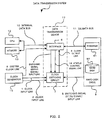
- the data transmission system includes the memory 13 which stores data, the hard disk drive 8 (which is also, hereinafter, referred to as "HDD") which is a storage device, a data transmission device 17 which performs a data transmission process between the memory 13 and the HDD 8, a clock generator 15 which generates a clock signal used as a reference signal of operations of the system, an instruction command transmission, and a data transmission, and the CPU 12 which controls the operations of the system.
- the memory 13 which stores data
- the hard disk drive 8 which is also, hereinafter, referred to as "HDD"
- HDD hard disk drive 8
- data transmission device 17 which performs a data transmission process between the memory 13 and the HDD 8
- a clock generator 15 which generates a clock signal used as a reference signal of operations of the system, an instruction command transmission, and a data transmission
- the CPU 12 which controls the operations of the system.
- the data transmission device 17 includes an interface 6 (which is also, hereinafter, referred to as "I/F") which enables to perform a data transmission process by connecting the HDD 8 to the memory 13, and a clock switching circuit 7 which switches a clock signal supplied to the I/F 6.
- the HDD 8 includes a hard disk 82 which stores data transmitted from the memory 13, and various registers 81 which store various instructions sent from the CPU 12.
- the I/F 6 is connected to the memory 13 and the CPU 12 via an internal data bus 10, and is connected to the HDD 8 via an IDE data bus 11. Further, to the I/F 6, a system clock generated by the clock generator 15 is supplied via a system clock line 9. A soft-reset register may be located in the I/F 6 to remove noise which occurs on switching the clock signal.
- an access clock signal (which is used to access) which is generated by the clock generator 15 is supplied via a clock input line 1
- a transmission clock signal (which is used to transmit) which has a frequency higher than a frequency of the access clock signal is supplied via a clock input line 2.
- a switching signal (for example, INTRQ signal) which prompts to switch from the access clock signal to the transmission clock signal is supplied to the circuit 7 via a switching signal input line 5.
- a status read signal which is used to access a status register in the register 81 is supplied to the circuit 7 via a status control signal line 16
- another switching signal for example, an error signal of the status register
- a clock signal is supplied to the I/F 6 via a clock output line 3.
- a command bus I/F 61 returns to the CPU 12, via a command bus, a notification showing whether commands supplied from the CPU 12 via the command bus are sent to the HDD 8 and various commands are entered from the HDD 8.
- the data bus I/F 62 receives data supplied from the memory 13 via a data bus and sends them to the HDD 8 via the IDE data bus 11, and receives data supplied from the HDD 8 via the IDE data bus 11 and sends them to the memory 13 via the data bus.
- the IDE I/F 63 outputs commands and data supplied from the command bus I/F 61 and the data bus I/F 62 to the HDD 8, and outputs notifications and data supplied form the HDD 8 to the command bus I/F 61 and the data bus I/F 62.
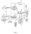
- the clock switching circuit 7 includes a flip-flop circuit 71 (which is also, hereinafter, referred to as "FF"), an enable circuit 72, an enable circuit 73, an enable circuit 74, and an enable circuit 75.
- FF flip-flop circuit
- the FF 71 is connected to an internal power supply V DD and outputs a signal in response to the switching signal supplied via the switching signal input line 5 and the status read signal supplied from the status control signal line 16.
- the enable circuit 72 inputs an output signal of the FF 71 and a switching signal supplied via the switching signal input line 4.
- the enable circuit 73 inputs an output signal of the enable circuit 72 and the access clock signal supplied via clock input line 1.
- the enable circuit 74 inputs an output signal of the enable circuit 72 and the transmission clock signal supplied via the clock input line 2.
- the enable circuit 75 inputs an output signal of the enable circuit 73 and an output signal of the enable circuit 74.
- a system clock signal generated by the clock generator 15 is supplied to the I/F 6 via the system clock line 9.
- the access clock signal and the transmission clock signal, which are also generated by the clock generator 15, are supplied to the clock switching circuit 7 in the data transmission device 17.
- the access clock signal is supplied to the enable circuit 73 and the transmission clock signal is supplied to the enable circuit 74. Further, for example, the INTRQ signal and the status read signal are supplied to the FF 71, and the error signal of the status register 81.
- the clock switching circuit 7 inputs the access clock signal and the transmission clock signal, and outputs the access clock signal to the I/F 6.
- the instruction commands are supplied to the I/F 6 in the data transmission device 17 via the command bus of the internal data bus 10.
- the I/F 6 receives the instruction commands from the CPU 12, the I/F 6 sends the instruction commands to the IDE data bus 11 via the command bus I/F 61 and the IDE I/F 63, and outputs the status read signal to the status control signal line 16.
- the status read signal supplied to the status control signal line 16 is entered to the clock switching circuit 7 and a reset operation of the FF 71 is performed. Also, the instruction commands supplied to the IDE data bus 11 is entered to the HDD 8. Thus, the instruction commands generated by the CPU 12 are transmitted to the HDD 8 (step S1).
- the HDD 8 When the HDD 8 receives the instruction commands, the HDD 8 stores the instruction commands into a command register in the register 81.
- the instruction commands supplied form the CPU 12 for example, are not stored successfully, a retransmission request is issued from the HDD 8 to the CPU 12 (step S2). After that, the procedure returns to step S1, and the CPU 12 retransmits the instruction commands to the HDD 8.
- the data transmission device 17 determines whether or not the instruction commands are successfully stored into the HDD 8 (step S2).
- the I/F 6 sends the notification (a switching signal) to the clock switching circuit 7 via the switching signal input line 4.
- the enable circuit 72 in the clock switching circuit 7 receives the switching signal via the switching signal input line 4, the enable circuit 72 detects that a switching signal on the switching signal input line 4 is changed.
- the circuit 72 in response to the reception, stops supplying of the access clock signal by using a mask and starts supplying of the transmission clock signal to the I/F 6 (step S3).
- the I/F 6 sends back a notification showing that the instruction commands are successfully transmitted to the command register, to the CPU 12.
- the CPU 12 instructs the memory 13 to transmit data stored in the memory 13 to the HDD 8.
- the memory 13 outputs the data to the internal data bus 10 according to the instruction of the CPU 12.
- the data supplied to the internal data bus 10 are then entered to the I/F 6 in the data transmission device 17.
- the I/F 6 sends the data to the IDE data bus 11 via the data bus I/F 62 and IDE I/F 63.
- the data stored in the memory 13 are transmitted to the HDD 8 (step S4).
- the HDD 8 stores the transmitted data.
- the HDD 8 issues a retransmission request to the memory 13 via the CPU 12 (step S5).
- the procedure returns to step S4 and data are retransmitted from the memory 13 to the HDD 8.
- the HDD 8 sends a notification (switching signal) showing that the transmission is completed successfully, to the data transmission device 17.
- the notification is sent to the clock switching circuit 7 via the switching signal input line 5.
- the FF 71 in the clock switching circuit 7 detects a change of a signal on the switching signal input line 5
- the FF 71 suspends supplying of the transmission clock signal by using a mask, and starts supplying the access clock signal to the I/F 6 (step S6).
- the I/F 6 sends back to the CPU 12 a notification showing that the data are successfully transmitted to the HDD 8, and then a series of transmission operations is completed. Therefore, at this time, HDD 8 becomes in a condition that instructions can be acceptable or a register access protocol can be performed.
- the I/F 6 can notify the CPU 12 of the completion of a data transmission process by returning a status read signal in response to a request of the CPU 12.
- the CPU 12 issues a switch instruction of the clock signal to the I/F 6.
- the HDD 8 includes a command register, a data register, and other various registers, and the CPU 12 may transmit various instructions (commands, parameters) to the other various register in the HDD 8. At the transmission of the various instructions, the access clock signal is used.
- the switching signal to prompt to switch the clock signal may be, for example, an error signal of a status register used in an IDE, or an INTRQ signal.
- the HDD 8 may generate switching signal in response to a completion of transmission of the instruction command or the data, and send the switching signal to the data transmission device 17.
- a data transmission system can be configured as shown in Fig. 6.
- the clock switching circuit 7 is not prepared, and the access clock signal or the transmission clock signal can be generated by the clock generator 15 using a software program and sent to the I/F 6.
- a data transmission system can be configured as shown in Fig. 7.
- the clock generator 15 does not generate both the access clock signal and the transmission clock signal.
- the clock generator 15 sends the access clock signal to the clock switching circuit 7 and the frequency divider 14 in parallel. Then, the frequency divider 14 divides the access clock signal to generate the data transmission signal.
- a data transmission rate can be increased at ATA/ATAPI (AT attachment/AT attachment packet interface) without departing from a standard, by switching a transmission clock using an IDE interface. Also, in this case, a size of a circuit is almost unchanged, since only an addition of a clock switching circuit is required.
- ATA/ATAPI AT attachment/AT attachment packet interface
- the data transmission system embodying the invention includes a clock generator which generates a clock signal used for data transmission and a clock signal used for instruction command transmission.
- the system can perform high speed data transmission between a device and a memory without changing a frequency of a system clock, since the data are transmitted from the memory to the device using the clock signal used for data transmission, after the instruction command is transmitted from a CPU to the device using the clock signal used for the instruction command transmission.
Landscapes
- Engineering & Computer Science (AREA)
- Theoretical Computer Science (AREA)
- Physics & Mathematics (AREA)
- General Engineering & Computer Science (AREA)
- General Physics & Mathematics (AREA)
- Information Transfer Systems (AREA)
- Synchronisation In Digital Transmission Systems (AREA)
Abstract
Description
Claims (12)
- A data transmission system comprising:a data transmission device (17) which transmits data stored in a memory (13) or an instruction command generated by a CPU (12) to a storage device (8); anda clock generator (15) which generates a first clock signal and a second clock signal which has a frequency lower than that of the first clock signal, wherein the data transmission device (17) transmits the instruction command from the CPU (12) to the storage device (8) by using the second clock signal, and after that, transmits the data from the memory (13) to the storage device (8) by using the first clock signal.
- The data transmission system of claim 1, wherein the data transmission device (17) transmits the data which are transmitted to and stored in the storage device (B), to the memory (13) by using the first clock signal.
- The data transmission system of claim 1, wherein the storage device (8) is a hard disk drive.
- The data transmission system of claim 1 or 2, wherein the data transmission device (17) comprises an interface (6) which transmits the data to the storage device (8) by using the first clock signal, and transmits the instruction command to the storage device (8) by using the second clock signal.
- The data transmission system of claim 1, 2 or 3, wherein the storage device (8) includes a status register (81) and the first clock signal is used on accessing the status register (81).
- The data transmission system of claim 4, wherein the interface (6) change a clock signal from the first clock signal to the second clock signal, or from the second clock signal to the first signal, based on a signal supplied in response to a notification that the storage device successfully receives the data or the instruction command.
- A method of transmitting data in a data transmission system having a data transmission device (17) which transmits data stored in a memory (13) or an instruction command generated by a CPU (12) to a storage device (8), comprising the steps of:generating, at a clock generator (15), a first clock signal, and a second clock signal which has a freqnency lower than that of the first clock signal;transmitting, at the data transmission device (17), the instruction command from the CPU (12) to the storage device (8) by using the second clock signal; andtransmitting, at the data transmission device (17), the data from the memory (13) to the storage device (8) by using the first clock signal.
- The method of claim 7 further comprising the step of:transmitting, at the data transmission device (17), the data which are transmitted to and stored in the storage device (8), to the memory (13) by using the first clock signal.
- The method of claim 7 or 8, wherein changing of the clock signals at the data transmission device (17) is performed in response to a notification that the storage device successfully receives the data or the instruction command.
- A recording medium readable by a computer, tangibly embodying a program of instructions executable by the computer to perform a method of transmitting data in a data transmission system having a data transmission device (17) which transmits data stored in a memory (13) or an instruction command generated by a CPU (12) to a storage device (8), comprising the steps of:generating, at a clock generator (15), a first clock signal, and a second clock signal which has a frequency lower than that of the first clock signal;transmitting, at the data transmission device (17), the instruction command from the CPU (12) to the storage device (8) by using the second clock signal; andtransmitting, at the data transmission device (17), the data from the memory (13) to the storage device (8) by using the first clock signal.
- A computer data signal embodied in a carrier wave and representing a sequence of instructions which, when executed by a processor, cause the processor to perform a method of transmitting data in a data transmission system having a data transmission device (17) which transmits data stored in a memory (13) or an instruction command generated by a CPU (12) to a storage device (8), comprising the steps of:generating, at a clock generator (15), a first clock signal, and a second clock signal which has a frequency lower than that of the first clock signal;transmitting, at the data transmission device (17), the instruction command from the CPU (12) to the storage device (8) by using the second clock signal; andtransmitting, at the data transmission device (17), the data from the memory (13) to the storage device (8) by using the first clock signal.
- A program product comprising, computer readable instructions and a recording medium bearing the computer readable instructions, the instructions being adaptable to enable a computer to perform a method of transmitting data in a data transmission system having a data transmission device (17) which transmits data stored in a memory (13) or an instruction command generated by a CPU (12) to a storage device (8), comprising the steps of:generating, at a clock generator (15), a first clock signal, and a second clock signal which has a frequency lower than that of the first clock signal;transmitting, at the data transmission device (17), the instruction command from the CPU (12) to the storage device (8) by using the second clock signal; andtransmitting, at the data transmission device (17), the data from the memory (13) to the storage device (8) by using the first clock signal.
Applications Claiming Priority (2)
| Application Number | Priority Date | Filing Date | Title |
|---|---|---|---|
| JP2001006777 | 2001-01-15 | ||
| JP2001006777A JP2002215333A (en) | 2001-01-15 | 2001-01-15 | Data transfer system, and computer provided with the same |
Publications (2)
| Publication Number | Publication Date |
|---|---|
| EP1231542A2 true EP1231542A2 (en) | 2002-08-14 |
| EP1231542A3 EP1231542A3 (en) | 2005-07-20 |
Family
ID=18874615
Family Applications (1)
| Application Number | Title | Priority Date | Filing Date |
|---|---|---|---|
| EP02250271A Withdrawn EP1231542A3 (en) | 2001-01-15 | 2002-01-15 | Data transmission system |
Country Status (3)
| Country | Link |
|---|---|
| US (1) | US20020095558A1 (en) |
| EP (1) | EP1231542A3 (en) |
| JP (1) | JP2002215333A (en) |
Cited By (1)
| Publication number | Priority date | Publication date | Assignee | Title |
|---|---|---|---|---|
| CN108509365A (en) * | 2018-01-23 | 2018-09-07 | 东莞市爱协生智能科技有限公司 | A kind of data transmission method and system of DBI |
Families Citing this family (5)
| Publication number | Priority date | Publication date | Assignee | Title |
|---|---|---|---|---|
| US7278047B2 (en) * | 2002-10-14 | 2007-10-02 | Lexmark International, Inc. | Providing different clock frequencies for different interfaces of a device |
| DE10329395A1 (en) * | 2003-06-30 | 2005-02-10 | Infineon Technologies Ag | Method for data transmission |
| JP5277562B2 (en) * | 2007-04-19 | 2013-08-28 | 株式会社ニコン | Electronic device, electronic camera and data transfer program |
| CN102129414B (en) * | 2010-01-15 | 2013-12-04 | 华为技术有限公司 | Variable frequency bus adapter, adapting method and system |
| TWI482030B (en) * | 2011-06-21 | 2015-04-21 | Via Tech Inc | Apparatus and method for advanced synchronous strobe transmission, optimized synchronous strobe transmission mechanism, apparatus and method for delayed synchronous data reception, optimized synchronized data reception mechanism, programmable mechanism f |
Family Cites Families (3)
| Publication number | Priority date | Publication date | Assignee | Title |
|---|---|---|---|---|
| GB2252432B (en) * | 1991-02-01 | 1994-09-28 | Intel Corp | Method and apparatus for operating a computer bus using selectable clock frequencies |
| JPH08235111A (en) * | 1994-12-26 | 1996-09-13 | Toshiba Corp | Computer system |
| US5784390A (en) * | 1995-06-19 | 1998-07-21 | Seagate Technology, Inc. | Fast AtA-compatible drive interface with error detection and/or error correction |
-
2001
- 2001-01-15 JP JP2001006777A patent/JP2002215333A/en active Pending
-
2002
- 2002-01-14 US US10/047,283 patent/US20020095558A1/en not_active Abandoned
- 2002-01-15 EP EP02250271A patent/EP1231542A3/en not_active Withdrawn
Cited By (1)
| Publication number | Priority date | Publication date | Assignee | Title |
|---|---|---|---|---|
| CN108509365A (en) * | 2018-01-23 | 2018-09-07 | 东莞市爱协生智能科技有限公司 | A kind of data transmission method and system of DBI |
Also Published As
| Publication number | Publication date |
|---|---|
| US20020095558A1 (en) | 2002-07-18 |
| EP1231542A3 (en) | 2005-07-20 |
| JP2002215333A (en) | 2002-08-02 |
Similar Documents
| Publication | Publication Date | Title |
|---|---|---|
| US7328356B2 (en) | Apparatus and method for saving power in a disk drive with a serial ATA interface connected to a host via a serial ATA bus | |
| US7107343B2 (en) | Method and apparatus for improved RAID 1 write performance in low cost systems | |
| US10268606B2 (en) | Method, device and system for switching access modes for data storage device | |
| JP2006164012A (en) | Data storage device and power save mode control method thereof | |
| US20050076162A1 (en) | Information processing device and method | |
| US10013367B2 (en) | I/O processing system including dynamic missing interrupt and input/output detection | |
| EP1231542A2 (en) | Data transmission system | |
| US20050102468A1 (en) | Methods and systems for coupling multiple initiators to SATA storage devices | |
| JP2015161999A (en) | Storage device, control apparatus, and control program | |
| US20030145150A1 (en) | Interface conversion system and data transfer method | |
| KR20040041623A (en) | Bus system and bus interface for connection to a bus | |
| EP1118942B1 (en) | Method of and system for managing reselection on a scsi bus | |
| JPH10207824A (en) | Timing mode selector for direct memory access transmission system | |
| CN116881091A (en) | System event log reporting method, device, chip, equipment and storage medium | |
| JP3930990B2 (en) | Computer system with interface between memory and peripheral device and method for selecting a communication parameter set | |
| CN113495682B (en) | System and method for queuing device management configuration requests | |
| JPH0816321A (en) | Interface circuit for data-transfer control and magnetic disk device | |
| US8782366B2 (en) | Executing host data transfer operations during setup of copy services operations | |
| JP2001337913A (en) | Data transfer system and its devices | |
| US7085864B1 (en) | Method and structure for handling packetized SCSI protocol data overruns in a multi-data channel host adapter | |
| JPH06301607A (en) | Multi-access I / O control method | |
| JP3260515B2 (en) | Interface circuit for multiple port storage device | |
| JP2006053928A (en) | Method for setting communication parameters between host system and peripheral device | |
| JP2008118211A (en) | Data transfer apparatus and data transfer method | |
| JP2003058323A (en) | Disk array device, its data transfer method, data transfer program |
Legal Events
| Date | Code | Title | Description |
|---|---|---|---|
| PUAI | Public reference made under article 153(3) epc to a published international application that has entered the european phase |
Free format text: ORIGINAL CODE: 0009012 |
|
| AK | Designated contracting states |
Kind code of ref document: A2 Designated state(s): AT BE CH CY DE DK ES FI FR GB GR IE IT LI LU MC NL PT SE TR |
|
| AX | Request for extension of the european patent |
Free format text: AL;LT;LV;MK;RO;SI |
|
| RAP1 | Party data changed (applicant data changed or rights of an application transferred) |
Owner name: NEC ELECTRONICS CORPORATION |
|
| PUAL | Search report despatched |
Free format text: ORIGINAL CODE: 0009013 |
|
| AK | Designated contracting states |
Kind code of ref document: A3 Designated state(s): AT BE CH CY DE DK ES FI FR GB GR IE IT LI LU MC NL PT SE TR |
|
| AX | Request for extension of the european patent |
Extension state: AL LT LV MK RO SI |
|
| 17P | Request for examination filed |
Effective date: 20060120 |
|
| AKX | Designation fees paid |
Designated state(s): FR GB |
|
| REG | Reference to a national code |
Ref country code: DE Ref legal event code: 8566 |
|
| 17Q | First examination report despatched |
Effective date: 20090826 |
|
| STAA | Information on the status of an ep patent application or granted ep patent |
Free format text: STATUS: THE APPLICATION HAS BEEN WITHDRAWN |
|
| 18W | Application withdrawn |
Effective date: 20091021 |