EP1231495A2 - Imaging device and method for producing the same - Google Patents
Imaging device and method for producing the same Download PDFInfo
- Publication number
- EP1231495A2 EP1231495A2 EP02250844A EP02250844A EP1231495A2 EP 1231495 A2 EP1231495 A2 EP 1231495A2 EP 02250844 A EP02250844 A EP 02250844A EP 02250844 A EP02250844 A EP 02250844A EP 1231495 A2 EP1231495 A2 EP 1231495A2
- Authority
- EP
- European Patent Office
- Prior art keywords
- optical member
- imaging device
- reflected light
- imaging
- convex mirror
- Prior art date
- Legal status (The legal status is an assumption and is not a legal conclusion. Google has not performed a legal analysis and makes no representation as to the accuracy of the status listed.)
- Granted
Links
Images




Classifications
-
- G—PHYSICS
- G03—PHOTOGRAPHY; CINEMATOGRAPHY; ANALOGOUS TECHNIQUES USING WAVES OTHER THAN OPTICAL WAVES; ELECTROGRAPHY; HOLOGRAPHY
- G03B—APPARATUS OR ARRANGEMENTS FOR TAKING PHOTOGRAPHS OR FOR PROJECTING OR VIEWING THEM; APPARATUS OR ARRANGEMENTS EMPLOYING ANALOGOUS TECHNIQUES USING WAVES OTHER THAN OPTICAL WAVES; ACCESSORIES THEREFOR
- G03B17/00—Details of cameras or camera bodies; Accessories therefor
- G03B17/02—Bodies
- G03B17/17—Bodies with reflectors arranged in beam forming the photographic image, e.g. for reducing dimensions of camera
-
- G—PHYSICS
- G02—OPTICS
- G02B—OPTICAL ELEMENTS, SYSTEMS OR APPARATUS
- G02B5/00—Optical elements other than lenses
- G02B5/08—Mirrors
- G02B5/10—Mirrors with curved faces
-
- G—PHYSICS
- G02—OPTICS
- G02B—OPTICAL ELEMENTS, SYSTEMS OR APPARATUS
- G02B13/00—Optical objectives specially designed for the purposes specified below
- G02B13/06—Panoramic objectives; So-called "sky lenses" including panoramic objectives having reflecting surfaces
-
- G—PHYSICS
- G02—OPTICS
- G02B—OPTICAL ELEMENTS, SYSTEMS OR APPARATUS
- G02B17/00—Systems with reflecting surfaces, with or without refracting elements
- G02B17/02—Catoptric systems, e.g. image erecting and reversing system
- G02B17/06—Catoptric systems, e.g. image erecting and reversing system using mirrors only, i.e. having only one curved mirror
-
- H—ELECTRICITY
- H04—ELECTRIC COMMUNICATION TECHNIQUE
- H04N—PICTORIAL COMMUNICATION, e.g. TELEVISION
- H04N23/00—Cameras or camera modules comprising electronic image sensors; Control thereof
- H04N23/50—Constructional details
- H04N23/55—Optical parts specially adapted for electronic image sensors; Mounting thereof
-
- H—ELECTRICITY
- H04—ELECTRIC COMMUNICATION TECHNIQUE
- H04N—PICTORIAL COMMUNICATION, e.g. TELEVISION
- H04N23/00—Cameras or camera modules comprising electronic image sensors; Control thereof
- H04N23/60—Control of cameras or camera modules
- H04N23/698—Control of cameras or camera modules for achieving an enlarged field of view, e.g. panoramic image capture
Definitions
- the present invention relates to an imaging device capable of imaging objects in the omniazimuthal angle of 360 degrees and used in the fields of visual systems such as, for example, surveillance cameras; and a method for producing the same.
- a generally used camera which has a limited viewing angle, is not suitable for such applications. Therefore, cameras using fish-eye lenses or other wide-angle lenses have been developed.
- convex mirrors having a shape of solid of revolution (such as conical mirrors), spherical mirrors or the like, have been actively studied.
- convex rotatable mirrors According to systems studied in this field, an optical image of a viewing angle of 360 degrees is taken by a convex rotatable mirror, then the optical image is converted into a video image, and the video image is further converted into a desirable image by a computer.
- Figure 8A shows a schematic structure of an imaging device 80 using a conventional convex rotational mirror
- Figure 8B is a cross-sectional view thereof taken along a plane including the rotation axis of a convex rotational mirror 93 described below.
- the imaging device 80 includes a convex rotational mirror unit 91.
- the convex rotational mirror unit 91 includes a generally disc-shaped base 92 and the generally conical convex rotational mirror 93.
- the imaging device 80 further includes a generally cup-shaped, spherical optical member 94.
- the optical member 94 is open toward the convex rotational mirror unit 91 and covers a surface of the base 92 and the convex rotational mirror 93.
- the optical member 94 holds the convex rotational mirror unit 91 and is formed of a light-transmissive material.
- An inner circumferential surface of the optical member 94 and the convex rotational mirror 93 interpose a hollow space therebetween.
- the optical member 94 has a thickness which is sufficiently thin to allow light which is incident on an outer circumferential surface of the optical member 94 to be transmitted through the optical member 94, so that it is proximately parallel to light which is directed toward the convex rotational mirror 93 from the inner circumferential surface of the optical member 94.
- a generally cylindrical imaging mechanism 98 is provided on the opposite side to the convex rotational mirror unit 91, with the optical member 94 interposed therebetween.
- the imaging mechanism 98 is able to be engaged with the optical member 94.
- the imaging mechanism 98 includes a lens 99 facing an opening of the optical member 94, which is formed on the opposite side to the convex rotational mirror unit 91, and an imaging section 90 provided on the opposite side to the optical member 94, with the lens 99 interposed therebetween.
- the imaging section 90 is connected to a signal processing section 88 provided for adjusting the distortion of an image taken by the imaging mechanism 98.
- the light-transmissive optical member 94 is used for holding the convex rotational mirror unit 91, and thus a separate holding member is not provided. The reason is that if a separate holding member is provided for holding the convex rotational mirror unit 91, an image of the holding member itself would be taken and so would be a part of an image taken by the imaging mechanism 98.
- the convex rotational mirror 93 a mirror which reflects incident light at a surface thereof is used so that an image formed by the reflection does not overlap the image that is intended to be taken.
- the convex rotational mirror 93 is formed of a metal material.
- the convex rotational mirror 93 may have a metal material, for example, vapor-deposited or plated onto an outer circumferential surface thereof.
- the imaging device 80 having the above-described structure operates as follows.
- Light 71 is incident on the outer circumferential surface of the light-transmissive optical member 94 and is transmitted through the optical member 94. While being transmitted through the optical member 94, the incident light 71 is refracted twice (not shown) so as to become light 72.
- the light 72 is directed from the inner circumferential surface of the optical member 94 toward the convex rotational mirror 93 through the hollow space between the optical member 94 and the convex rotational mirror 93. Then, the light 72 is reflected by the convex rotational mirror 93 and is directed toward the imaging mechanism 98 as reflected light 81.
- the reflected light 81 is transmitted through the lens 99 of the imaging mechanism 98 and incident on the imaging section 90.
- the imaging section 90 transforms the reflected light 81 into an image signal representing an image and outputs the image signal to the signal processing section 88.
- the signal processing section 88 processes the received image signal so as to adjust the distortion of the image.
- the conventional imaging device 80 has the following problems.
- an imaging device includes a convex mirror for reflecting incident light representing an object, the convex mirror having a shape of solid of revolution; an imaging mechanism for taking an image represented by reflected light from the convex mirror; and an optical member for guiding the incident light toward the convex mirror and guiding the reflected light toward the imaging mechanism, the optical member being in close-contact with the convex mirror.
- the optical member has a concave portion which is in close-contact with the convex mirror so as to cover the convex mirror.
- the convex mirror is formed of a thin layer of a material having a mirror-surface effect, the thin layer being provided on the concave portion.
- the convex mirror is formed of a metal material.
- the convex mirror is formed of aluminum.
- the convex mirror is formed as a result of vapor-deposition, sputtering or plating of a material having a mirror-surface effect.
- the imaging mechanism includes a lens for converging the reflected light, and an imaging section for taking an image represented by the reflected light converged by the lens; and the lens is integrally formed with the optical member.
- the imaging mechanism includes a lens for converging the reflected light, and an imaging section for taking an image represented by the reflected light converged by the lens; and the lens is in close-contact with the optical member.
- the optical member has a refractive index which is smaller than the refractive index of the lens.
- the optical member has an outer circumferential surface formed so as to cause the incident light to be incident thereon in a direction normal to the outer circumferential surface.
- the optical member has a reflected light releasing face formed so as to cause the reflected light directed toward the imaging mechanism to be incident thereon in a direction normal to the reflected light releasing face.
- the reflected light releasing face is a part of a surface of a circle having, as the center, a focal point at which the reflected light is converged.
- a method for producing the above-described imaging device includes the steps of causing the optical member to be in close-contact with the convex mirror so that the optical member covers the convex mirror; and attaching the imaging mechanism to the optical member so that the reflected light is incident on the imaging mechanism.
- the optical member formed of a light-transmissive material is provided in close-contact with a surface of the convex rotational mirror, so as to cover the convex rotational mirror. Therefore, even when the imaging device is subjected to external heat, ultraviolet rays or the like, the surface of the convex rotational mirror is not deteriorated due to oxidation or the like, nor is the vapor-deposited or plated metal material exfoliated. Thus, the reflectance of the convex rotational mirror is not reduced. Since the optical member is provided in close-contact with the convex rotational mirror so as to cover the convex rotational mirror, dust, moisture or the like can be prevented from entering between the convex rotational mirror and the optical member.
- the structure of the optical member in close-contact with the convex rotational mirror also increases the mechanical strength of the optical member compared to the conventional structure having the hollow optical member, thus providing a wider viewing angle.
- the optical member In a structure where the optical member is formed of a material having a smaller refractive index than that of the lens, the optical member need not be formed of a material having a large refractive index and thus need not be expensive, as described below in a second example of the present invention.
- the optical member and the lens are formed of the same material, the optical member and the lens can be integrally formed. Therefore, the adjustment of the lens with respect to the optical member is not necessary and the number of components of the optical system can be reduced, as described below in a first example of the present invention.
- the optical system can be easily designed as described below in a third example of the present invention ( Figures 5 and 6 ).
- the reflected light is designed to be converged on a prescribed focal point
- the reflected light releasing face may be formed so as to be a part of the surface of a circle having the focal point as the center.
- the thin layer acts as a convex rotational mirror.
- the convex rotational mirror and the optical member can be integrally produced and the size of the imaging device is reduced. The production process of the imaging device is also simplified.
- the convex rotational mirror may be formed of a convex surface of a member formed of a metal material.
- Aluminum, silver, platinum, a nickel-chromium alloy, gold and the like are suitable metal materials for producing a mirror-surface effect. Aluminum is optimum to reduce the cost of the imaging device.
- the invention described herein makes possible the advantages of providing (1) an imaging device for preventing reduction in the reflectance of light incident on a convex rotational mirror, and a method for producing the same; and (2) an imaging device for preventing dust, moisture or the like from entering between a convex rotational mirror and an optical member, and a method for producing the same.
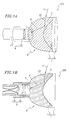
- Figure 1A shows a schematic structure of an imaging device 100 according to a first example of the present invention
- Figure 1B is a cross-sectional view thereof taken along a plane including the rotation axis of a convex rotational mirror 3 described below.
- the imaging device 100 includes a convex rotational mirror unit 1.
- the convex rotational mirror unit 1 includes a generally disc-shaped base 2 and the convex rotational mirror 3 provided on a surface of the base 2.
- the convex rotational mirror 3 has a rotational shape having a rotation axis which is vertical to the surface of the base 2.
- a surface of the convex rotational mirror 3 is, for example, hyperboloidal.
- the surface of the convex rotational mirror 3 may be hemispherical or conical.
- the convex rotational mirror 3 is formed of a metal material such as, for example, aluminum or stainless steel.
- the convex rotational mirror 3 may have a material having a mirror-surface effect such as, for example, aluminum, silver, platinum, a nickel-chromium alloy or gold, vapor-deposited, sputtered or plated onto the surface thereof.
- the imaging device 100 further includes an optical member 4 so as to cover the surface of the base 2 and the convex rotational mirror 3.
- a surface of the optical member 4 facing the convex rotational mirror unit 1 has a concave portion 5 having a curved surface projecting in an opposite direction to the base 2.
- the optical member 4 is formed of, for example, a light-transmissive and non-moisture permeable resin such as an acrylic resin, polycarbonate, or the like, or glass.
- the optical member 4 is formed so as to be in close-contact with the convex rotational mirror 3 along the concave portion 5, unlike in the conventional imaging device 80 described above with reference to Figures 8A and 8B which have a hollow space between the optical member 94 and the convex rotational mirror 93.
- the optical member 4 preferably has a rotational shape with a rotation axis that matches the rotation axis of the convex rotational mirror 3. The reason for this is because where the optical member 4 and the convex rotational mirror 3 have matching rotation axes, the optical path length from an outer circumferential surface of the optical member 4 to a surface of the convex rotational mirror 3 is equal over the omniazimuthal angle of 360 degrees. This facilitates a processing operation of an image signal obtained based on light which is reflected by the convex rotational mirror 3 and represents an image of an object.
- the imaging device 100 further includes a generally cylindrical imaging mechanism 8 on the opposite side to the convex rotational mirror unit 1, with the optical member 4 interposed therebetween.
- the imaging mechanism 8 includes a lens 9 facing a reflected light releasing face 7 of the optical member 4, which is formed on the opposite side to the convex rotational mirror unit 1.
- the lens 9 is located so that an optical axis thereof matches the rotation axis of the convex rotational mirror 3.
- the lens 9 converges light which is reflected by the convex rotational mirror 3.
- the imaging mechanism 8 also includes an imaging section 10 provided on the opposite side to the optical member 4 with the lens 9 interposed therebetween.
- the imaging section 10 is formed of a CCD or the like.
- the imaging section 10 generates an image signal representing an image based on the reflected light converged by the lens 9, and outputs the image signal to a signal processing section (not shown).
- the signal processing section adjusts the distortion of the image signal which is output from the imaging section 10.
- the imaging device 100 having the above-described structure, operates as follows.
- Light 21 is incident on the outer circumferential surface of the optical member 4.
- the incident light 21 is refracted by the outer circumferential surface of the optical member 4 so as to become light 22.
- the light 22 passes through the optical member 4 and reaches the convex rotational mirror 3 which is in close-contact with the optical member 4.
- the light-transmissive resin such as an acrylic resin, polycarbonate or the like, or glass that is used to form the optical member 4, has a refractive index which is larger than that of air at room temperature.
- a light-transmissive resin has a refractive index of 1.49 to 1.71, and glass has a refractive index of 1.52 to 1.90. Therefore, the viewing angle of the imaging device 100 is wider than that of the conventional imaging device 80 ( Figures 8A and 8B ) having a hollow space filled with air between the optical member 94 and the convex rotational mirror 93.
- the light 22 incident on the convex rotational mirror 3 is reflected by the surface of the convex rotational mirror 3 so as to become reflected light 41.
- the reflected light 41 passes through the reflected light releasing face 7 of the optical member 4 and is converged by the lens 9 of the imaging mechanism 8.
- the imaging section 10 generates an image signal which represents an image based on the reflected light 41 converged by the lens 9, and outputs the image signal to the signal processing section (not shown).
- the signal processing section adjusts the distortion of the image signal which is output from the imaging section 10.
- the optical member 4 is in close-contact with the convex rotational mirror 3. Therefore, there is no air or moisture existing between the optical member 4 and the convex rotational mirror 3, unlike the conventional imaging device 80 described above with reference to Figures 8A and 8B. Due to such a structure, the surface of the convex rotational mirror 3 is prevented from being corroded by moisture or air.
- a thin layer of a material having a mirror-surface effect may be formed on a surface of the concave portion 5 of the optical member 4, instead of the convex rotational mirror unit 1 being provided.
- the light 22 is reflected by the thin layer.
- a layer of a resin or other light-transmissive materials may be formed on a surface of the thin layer opposite to the surface reflecting the light 22.
- the convex rotational mirror 3 and the optical member 4 may be produced separately.
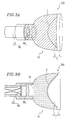
- Figure 2A shows a schematic structure of another imaging device 200 according to the first example of the present invention
- Figure 2B is a cross-sectional view thereof taken along a plane including the rotation axis of the convex rotation mirror 3.
- Identical elements described above referring to Figures 1A and 1B bear identical reference numerals therewith and detailed descriptions thereof will be omitted.
- the imaging device 200 includes an optical member 4A which is generally cylindrical. Such a structure provides an effect substantially the same as that of the imaging device 100.
- Figure 3A shows a schematic structure of still another imaging device 300 according to the first example of the present invention
- Figure 3B is a cross-sectional view thereof taken along a plane including the rotation axis of the convex rotation mirror 3.
- Identical elements described above referring to Figures 1A and 1B bear identical reference numerals therewith and detailed descriptions thereof will be omitted.
- the imaging device 300 includes an optical member 4B which is integrally formed with a lens 9B included in an imaging mechanism 8B.
- the optical member 4B is integrally formed with the lens 9B, the following advantages are provided.
- the production process can exclude the step of adjusting the position of the lens 9B with respect to the optical member 4, and also the number of components of the optical system can be reduced.
- the production efficiency is improved.
- the imaging devices 100, 200 and 300 also have the advantage of a higher mechanical strength since the optical members 4, 4A and 4B are solid inside.
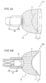
- Figure 4A shows a schematic structure of an imaging device 400 according to a second example of the present invention
- Figure 4B is a cross-sectional view thereof taken along a plane including the rotation axis of a convex rotational mirror 3.
- Identical elements described above referring to Figures 1A and 1B bear identical reference numerals therewith and detailed descriptions thereof will be omitted.
- An imaging device 400 includes an optical member 4C.
- the optical member 4C has a reflected light releasing face 7C on the opposite side to the convex rotational mirror unit 1.
- the reflected light releasing face 7C has a curved surface which projects toward the convex rotational mirror 3.
- the optical member 4C is formed of a light-transmissive material.
- a generally cylindrical imaging mechanism 8C is provided on the opposite side to the convex rotational mirror unit 1 with the optical member 4C interposed therebetween.
- the imaging mechanism 8C covers the reflected light releasing face 7C of the optical member 4C.
- the imaging mechanism 8 includes a lens 9C.
- the lens 9C is in close-contact with the reflected light releasing face 7C.
- the lens 9C is formed of a light-transmissive material.
- the light-transmissive material used to form the lens 9C has a refractive index which is larger than that of the light-transmissive material used to form the optical member 4C.
- the light-transmissive material used to form the lens 9C is, for example, lead glass having a refractive index of 1.92 or diamond having a refractive index of 2.42.
- the imaging device 400 having the above-described structure, operates as follows.
- Light which is incident on an outer circumferential surface of the optical member 4C , is refracted by the outer circumferential surface, passes through the optical member 4C and is directed to the convex rotational mirror 3 which is in close-contact with the optical member 4C.
- the light incident on the convex rotational mirror 3 is reflected by a surface of the convex rotational mirror 3 and passes through the reflected light releasing face 7C of the optical member 4C as reflected light, so as to be directly incident on the lens 9C, which is in close-contact with the reflected light releasing face 7C.
- the reflected light is then converged by the lens 9C.
- the imaging section 10 generates an image signal which represents an image based on the reflected light converged by the lens 9C, and outputs the image signal to the signal processing section (not shown).
- the signal processing section adjusts the distortion of the image signal which is output from the imaging section 10.
- the lens 9C is in close-contact with the optical member 4C. Therefore, the light reflected by the convex rotational mirror 3 is incident on the lens 9C from the reflected light releasing face 7C directly, instead of through the air layer, as in the imaging device 100 ( Figures 1A and 1B ), formed between the reflected light releasing face 7 and the lens 9.
- the refractive index of the optical member 4C, having the reflected light releasing face 7C in the imaging device 400, is larger than the refractive index of the air layer in the imaging device 100. Therefore, the curvature of the lens 9C directly receiving the incident light from the reflected light releasing face 7C needs to be larger than that of the lens 9 receiving the incident light through the air layer.
- the lens 9C is formed of lead glass, diamond or the like, which have a relatively large refractive index. Since a material possessing a larger refractive index is relatively expensive, the optical member 4C is formed of a material having a small refractive index and thus is relatively inexpensive.
- the reflected light releasing face 7C of the optical member 4C is in close-contact with the lens 9C of the imaging mechanism 8C, the following advantages are provided, which are similar to those of the imaging device 300, described above with reference to Figures 3A and 3B.
- the production process can exclude the step of adjusting the position of the lens 9C with respect to the optical member 4C, and also the number of components of the optical system can be reduced. Thus, the production efficiency is improved.
- FIGs 5 and 6 show a schematic structure of an imaging device 500 according to a third example of the present invention. Identical elements described above referring to Figures 1A and 1B bear identical reference numerals therewith and detailed descriptions thereof will be omitted.
- the imaging device 500 is different from the imaging device 100 ( Figures 1A and 1B ) in that the imaging device 500 includes an optical member 4D instead of the optical member 4.
- the optical member 4D has an outer circumferential surface formed so as to cause light to be incident thereon in a direction normal thereto ( Figure 5 ).
- the optical member 4D includes a reflected light releasing face 7D formed so as to cause the light reflected by the convex rotational mirror 3 to pass therethrough in a direction normal thereto ( Figure 6 ).
- the imaging device 500 having the above-described structure, operates as follows.
- the incident light 23 is then reflected by a surface of the convex rotational mirror 3 so as to become reflected light 42.
- the reflected light 42 passes straight through the reflected light releasing face 7D without being refracted and is converged by a lens (not shown) included in the imaging mechanism 8.
- An imaging section (not shown) of the imaging mechanism 8 generates an image signal representing an image based on the reflected light 42 converged by the lens, and outputs the image signal to a signal processing section (not shown).
- the signal processing section adjusts the distortion of the image signal which is output from the imaging section.
- the outer circumferential surface of the optical member 4D is formed so as to cause the light to be incident in a direction normal thereto. Therefore, the incident light 23 advances straight without being refracted by the outer circumferential surface, regardless of the refractive index of the material used to form the optical member 4D.
- the reflected light releasing face 7D is formed so as to cause light to pass therethrough in a direction normal thereto. Therefore, the reflected light 42 passes straight through the reflected light releasing face 7D without being refracted, regardless of the refractive index of the material used to form the optical member 4D. Accordingly, the optical system can be designed without considering the refractive index of the optical member 4D, with respect to the incident light or the reflected light. Since the material for the optical member 4D can be selected regardless of the refractive index, the optical system can be designed more easily.
- the convex rotational mirror 3 is designed so as to converge the reflected light 42 on a prescribed focal point.
- the reflected light releasing face 7D may be formed so as to be a part of the surface of a circle having the focal point as the center.
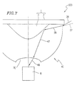
- FIG 7 is a cross-sectional view of another imaging device 600 according to the third example of the present invention. Identical elements described above referring to Figures 5 and 6 bear identical reference numerals therewith and detailed descriptions thereof will be omitted.
- the imaging device 600 is different from the imaging device 500 in that the imaging device 600 includes an optical member 4E instead of the optical member 4D.
- the optical member 4E has an outer circumferential surface formed to refract light incident thereon.
- the optical member 4E includes a reflected light releasing face 7E formed to refract the light reflected by the convex rotational mirror 3.
- the imaging device 600 having the above-described structure, operates as follows.
- the light 28 passes through the optical member 4E and is directed to the convex rotational mirror 3 which is in close-contact with the optical member 4E.
- the light 28 is then reflected by a surface of the convex rotational mirror 3 so as to become reflected light 47.
- the reflected light 47 is refracted by the reflected light releasing face 7E, is transmitted through the air layer between the reflected light releasing face 7E and the imaging mechanism 8 and is converged by a lens (not shown) included in the imaging mechanism 8.
- An imaging section (not shown) of the imaging mechanism 8 generates an image signal representing an image based on the reflected light 47 converged by the lens, and outputs the image signal to a signal processing section (not shown).
- the signal processing section adjusts the distortion of the image signal which is output from the imaging section.
- dashed line 27 represents incident light in the conventional imaging device 80 described above with reference to Figures 8A and 8B.
- the conventional imaging device 80 the light incident on the optical member 94 and the light directed from the optical member 94 toward the convex rotational mirror 93 are proximately parallel to each other due to the thinness of the hollow optical member 94.
- the incident light 27 becomes the light 28.
- the imaging device 600 in the third example of the present invention the light 26 is incident on the optical member 4E reaches the optical member 4E along a path above the path of the light 27. Therefore, the viewing angle of the imaging device 600 is wider than that of the conventional imaging device 80.
- the viewing angle of the imaging device can be enlarged.
- the influence of the reflected light inside the optical member is eliminated.
- the convex rotational mirror 3 has a hyperboloidal shape, the image data representing the image taken by the imaging mechanism can be easily converted into image data representing a perspective view or a panoramic view.
- the present invention provides an imaging device for preventing reduction in the reflectance of light incident on a convex rotational mirror, and a method for producing the same; and an imaging device for preventing dust, moisture or the like from entering between a convex rotational mirror and an optical member, and a method for producing the same.
Landscapes
- Physics & Mathematics (AREA)
- General Physics & Mathematics (AREA)
- Optics & Photonics (AREA)
- Engineering & Computer Science (AREA)
- Multimedia (AREA)
- Signal Processing (AREA)
- Lenses (AREA)
- Studio Devices (AREA)
- Stereoscopic And Panoramic Photography (AREA)
- Optical Elements Other Than Lenses (AREA)
Abstract
Description
Claims (16)
- An imaging device, comprising:a convex mirror for reflecting incident light representing an object, the convex mirror having a shape of solid of revolution;an imaging mechanism for taking an image represented by reflected light from the convex mirror; andan optical member for guiding the incident light toward the convex mirror and guiding the reflected light toward the imaging mechanism, the optical member being in close-contact with the convex mirror.
- An imaging device according to claim 1, wherein the optical member has a concave portion which is in close-contact with the convex mirror so as to cover the convex mirror.
- An imaging device according to claim 2, wherein the convex mirror is formed of a thin layer of a material having a mirror-surface effect, the thin layer being provided on the concave portion.
- An imaging device according to claim 1, wherein the convex mirror is formed of a metal material.
- An imaging device according to claim 1, wherein the convex mirror is formed of aluminum.
- An imaging device according to claim 1, wherein the convex mirror is formed as a result of vapor-deposition, sputtering or plating of a material having a mirror-surface effect.
- An imaging device according to claim 1, wherein the imaging mechanism includes a lens for converging the reflected light, and an imaging section for taking an image represented by the reflected light converged by the lens; and the lens is integrally formed with the optical member.
- An imaging device according to claim 1, wherein the imaging mechanism includes a lens for converging the reflected light, and an imaging section for taking an image represented by the reflected light converged by the lens; and the lens is in close-contact with the optical member.
- An imaging device according to claim 8, wherein the optical member has a refractive index which is smaller than the refractive index of the lens.
- An imaging device according to claim 1, wherein the optical member has an outer circumferential surface formed so as to cause the incident light to be incident thereon in a direction normal to the outer circumferential surface.
- An imaging device according to claim 1, wherein the optical member has a reflected light releasing face formed so as to cause the reflected light directed toward the imaging mechanism to be incident thereon in a direction normal to the reflected light releasing face.
- An imaging device according to claim 11, wherein the reflected light releasing face is a part of a surface of a circle having, as the center, a focal point at which the reflected light is converged.
- A method for producing an imaging device according to claim 1, the method comprising the steps of:causing the optical member to be in close-contact with the convex mirror so that the optical member covers the convex mirror; andattaching the imaging mechanism to the optical member so that the reflected light is incident on the imaging mechanism.
- An imaging device comprising
means providing a convex reflection surface having a shape of solid revolution for reflecting incident light, and
an image sensor for receiving the reflected light, wherein there is provided an optical member for conducting the incident light toward the reflection surface and for conducting the reflected light toward the image sensor, and wherein said reflection surface is contiguous with the body of the optical member. - An imaging device including a convex mirror and an optical element which conducts incident light right up to a reflection surface and conducts the reflected light toward an optical sensor.
- An imaging device according to claim 14 or claim 15 wherein said optical member comprises a solid body formed with a concave surface at which the reflection surface is provided, or with which the reflection surface is in contact.
Priority Applications (1)
| Application Number | Priority Date | Filing Date | Title |
|---|---|---|---|
| EP05008236A EP1564574A1 (en) | 2001-02-09 | 2002-02-07 | Imaging device and method for producing the same |
Applications Claiming Priority (2)
| Application Number | Priority Date | Filing Date | Title |
|---|---|---|---|
| JP2001034690 | 2001-02-09 | ||
| JP2001034690A JP3651844B2 (en) | 2001-02-09 | 2001-02-09 | Imaging device and manufacturing method thereof |
Related Child Applications (1)
| Application Number | Title | Priority Date | Filing Date |
|---|---|---|---|
| EP05008236A Division EP1564574A1 (en) | 2001-02-09 | 2002-02-07 | Imaging device and method for producing the same |
Publications (3)
| Publication Number | Publication Date |
|---|---|
| EP1231495A2 true EP1231495A2 (en) | 2002-08-14 |
| EP1231495A3 EP1231495A3 (en) | 2004-03-31 |
| EP1231495B1 EP1231495B1 (en) | 2007-05-02 |
Family
ID=18898247
Family Applications (2)
| Application Number | Title | Priority Date | Filing Date |
|---|---|---|---|
| EP02250844A Expired - Lifetime EP1231495B1 (en) | 2001-02-09 | 2002-02-07 | Imaging device and method for producing the same |
| EP05008236A Withdrawn EP1564574A1 (en) | 2001-02-09 | 2002-02-07 | Imaging device and method for producing the same |
Family Applications After (1)
| Application Number | Title | Priority Date | Filing Date |
|---|---|---|---|
| EP05008236A Withdrawn EP1564574A1 (en) | 2001-02-09 | 2002-02-07 | Imaging device and method for producing the same |
Country Status (6)
| Country | Link |
|---|---|
| US (1) | US6865029B2 (en) |
| EP (2) | EP1231495B1 (en) |
| JP (1) | JP3651844B2 (en) |
| KR (1) | KR100548744B1 (en) |
| DE (1) | DE60219839T2 (en) |
| TW (1) | TWI234007B (en) |
Cited By (7)
| Publication number | Priority date | Publication date | Assignee | Title |
|---|---|---|---|---|
| ITPD20110320A1 (en) * | 2011-10-10 | 2013-04-11 | Visus S R L I | DEVICE FOR RECOVERY OF 360 ° PANORAMIC IMAGES |
| ITVI20120003A1 (en) * | 2012-01-03 | 2013-07-04 | Pan Vision S R L | OPTICAL DEVICE FOR OBTAINING, IN A SINGLE ACQUISITION, THE FIELD OF VIEW OF A SPHERICAL CAP AND RELATED OPTICAL SYSTEM AND RECOVERY SYSTEM / SCREENING OF THREE-DIMENSIONAL IMAGES |
| ITVI20120002A1 (en) * | 2012-01-03 | 2013-07-04 | Pan Vision S R L | OPTICAL SYSTEM FOR ACHIEVING IN A SINGLE ACQUISITION OF A 360 ° PANORAMIC IMAGE AND RELATED EQUIPMENT FOR RECOVERY / PROJECTION OF SUCH IMAGE |
| ITVI20120004A1 (en) * | 2012-01-03 | 2013-07-04 | Pan Vision S R L | OPTICAL DEVICE FOR OBTAINING A MAGNIFICATION OF A CERTAIN AREA OF A 360 ° PANORAMIC VIEWING FIELD AND RELATED OPTICAL SYSTEM AND EQUIPMENT FOR RECOVERY / PROJECTION OF THREE-DIMENSIONAL IMAGES |
| WO2013102941A1 (en) * | 2012-01-03 | 2013-07-11 | Pan-Vision S.R.L. | Objective lens with hyper-hemispheric field of view |
| WO2013102943A1 (en) * | 2012-01-03 | 2013-07-11 | Pan-Vision S.R.L. | Environment monitoring device |
| WO2015004479A3 (en) * | 2013-07-12 | 2015-04-09 | Pano Pro Ltd | Adapter and casing apparatus for an imaging device |
Families Citing this family (37)
| Publication number | Priority date | Publication date | Assignee | Title |
|---|---|---|---|---|
| JP3690733B2 (en) * | 2001-02-09 | 2005-08-31 | シャープ株式会社 | Imaging device |
| KR100452754B1 (en) * | 2001-06-28 | 2004-10-12 | 주식회사세운메디칼상사 | Apparatus for inserting guide wire for use in catheter |
| US20060201351A1 (en) * | 2001-07-02 | 2006-09-14 | Gi View Ltd. | Self-propelled imaging system |
| US7399095B2 (en) * | 2003-07-09 | 2008-07-15 | Eyesee360, Inc. | Apparatus for mounting a panoramic mirror |
| US20050038318A1 (en) * | 2003-08-13 | 2005-02-17 | Benad Goldwasser | Gastrointestinal tool over guidewire |
| US20050036059A1 (en) * | 2003-08-13 | 2005-02-17 | Benad Goldwasser | Ingestible imaging system |
| WO2006072928A2 (en) * | 2005-01-06 | 2006-07-13 | G.I. View Ltd. | Gastrointestinal tool over guiding element |
| US7833176B2 (en) * | 2003-08-13 | 2010-11-16 | G. I. View Ltd. | Pressure-propelled system for body lumen |
| US7087011B2 (en) * | 2003-12-30 | 2006-08-08 | Gi View Ltd. | Gastrointestinal system with traction member |
| ES2546355T3 (en) * | 2004-01-09 | 2015-09-22 | G.I. View Ltd. | Pressure propelled system for body light |
| US7635346B2 (en) * | 2004-01-09 | 2009-12-22 | G. I. View Ltd. | Pressure-propelled system for body lumen |
| US8419678B2 (en) | 2004-01-09 | 2013-04-16 | G.I. View Ltd. | Pressure-propelled system for body lumen |
| US7635345B2 (en) * | 2004-01-09 | 2009-12-22 | G. I. View Ltd. | Pressure-propelled system for body lumen |
| EP1765142A4 (en) | 2004-05-14 | 2007-10-10 | G I View Ltd | Omnidirectional and forward-looking imaging device |
| US7593057B2 (en) * | 2004-07-28 | 2009-09-22 | Microsoft Corp. | Multi-view integrated camera system with housing |
| JP2006203494A (en) * | 2005-01-20 | 2006-08-03 | Nippon Seiki Co Ltd | Visual sensor |
| CN101541227B (en) * | 2005-02-10 | 2013-06-05 | G.I.视频有限公司 | Advancement techniques for gastrointestinal tool with guiding element |
| JP4585352B2 (en) * | 2005-03-31 | 2010-11-24 | オリンパス株式会社 | Optical system |
| WO2006120690A2 (en) * | 2005-05-13 | 2006-11-16 | G.I. View Ltd. | Endoscopic measurement techniques |
| KR100764235B1 (en) * | 2005-06-14 | 2007-10-05 | 나노광학(주) | Lateral radiation lens |
| US8430809B2 (en) * | 2005-08-01 | 2013-04-30 | G. I View Ltd. | Capsule for use in small intestine |
| WO2007015240A2 (en) * | 2005-08-01 | 2007-02-08 | G.I. View Ltd. | Tools for use in small intestine |
| WO2007015241A2 (en) * | 2005-08-01 | 2007-02-08 | G.I. View Ltd. | Tools for use in esophagus |
| JP2007147948A (en) * | 2005-11-28 | 2007-06-14 | Nippon Seiki Co Ltd | Imaging apparatus |
| US8072482B2 (en) | 2006-11-09 | 2011-12-06 | Innovative Signal Anlysis | Imaging system having a rotatable image-directing device |
| JP2010516325A (en) * | 2007-01-17 | 2010-05-20 | ジー・アイ・ヴュー・リミテッド | Diagnostic or therapeutic tool for colonoscopy |
| US10226600B2 (en) * | 2008-07-30 | 2019-03-12 | G.I. View Ltd. | System and method for enhanced maneuverability |
| CA2741206C (en) | 2008-11-03 | 2016-01-12 | G.I. View Ltd | Remote pressure sensing system and method thereof |
| US9430923B2 (en) | 2009-11-30 | 2016-08-30 | Innovative Signal Analysis, Inc. | Moving object detection, tracking, and displaying systems |
| CN103747166A (en) * | 2013-10-30 | 2014-04-23 | 樊书印 | Panorama lens of handset |
| US10139819B2 (en) | 2014-08-22 | 2018-11-27 | Innovative Signal Analysis, Inc. | Video enabled inspection using unmanned aerial vehicles |
| KR102489794B1 (en) * | 2014-09-15 | 2023-01-18 | 리모트리얼리티 코포레이션 | Compact panoramic camera:optical system, apparatus, image forming method |
| CN105739074A (en) * | 2016-03-29 | 2016-07-06 | 宁波舜宇光电信息有限公司 | Optical imaging device and condenser thereof |
| CA3017349C (en) * | 2016-03-10 | 2021-08-31 | Visbit Inc. | Time multiplexing programmable field of view imaging |
| CN107817592B (en) * | 2017-11-09 | 2024-03-08 | 刘超 | External lens |
| CN110192811A (en) * | 2019-01-15 | 2019-09-03 | 尚科宁家(中国)科技有限公司 | A kind of panoramic shooting module package structure |
| KR102397409B1 (en) * | 2021-12-31 | 2022-05-12 | 주식회사 제이시스 | Inspection system for railway ground facility using image processing technology and method thereof |
Family Cites Families (14)
| Publication number | Priority date | Publication date | Assignee | Title |
|---|---|---|---|---|
| GB190815188A (en) * | 1908-07-17 | 1909-06-10 | Improved Periscope Ltd | Improved Means or Apparatus whereby Objects can be Sighted or Photographed from Submarine Boats or other Situations. |
| HU192125B (en) * | 1983-02-08 | 1987-05-28 | Budapesti Mueszaki Egyetem | Block of forming image for centre theory projection adn reproduction of spaces |
| JPH02151828A (en) * | 1988-12-02 | 1990-06-11 | Mitsubishi Electric Corp | All-azimuth observation device |
| NL8901245A (en) * | 1989-05-19 | 1990-12-17 | Philips Nv | RETROFOKUS OBJECTIVE FLANGE AND OPTICAL SCANNER EQUIPPED WITH SUCH A LENS. |
| JP2825333B2 (en) | 1990-10-09 | 1998-11-18 | 株式会社レアックス | Integral cone mirror for hole wall observation and lifting sonde using this |
| US5745286A (en) * | 1995-10-13 | 1998-04-28 | Regents Of The University Of California | Forming aspheric optics by controlled deposition |
| KR100482727B1 (en) * | 1996-05-10 | 2005-09-02 | 더 트러스티스 오브 컬럼비아 유니버시티 인 더 시티 오브 뉴욕 | Omnidirectional imaging device and method |
| US6373642B1 (en) * | 1996-06-24 | 2002-04-16 | Be Here Corporation | Panoramic imaging arrangement |
| US6459451B2 (en) * | 1996-06-24 | 2002-10-01 | Be Here Corporation | Method and apparatus for a panoramic camera to capture a 360 degree image |
| JP3086204B2 (en) * | 1997-12-13 | 2000-09-11 | 株式会社アコウル | Omnidirectional imaging device |
| JPH11316343A (en) * | 1998-05-01 | 1999-11-16 | Nikon Corp | Catadioptric lens |
| JP4227249B2 (en) * | 1999-05-28 | 2009-02-18 | キヤノン株式会社 | Imaging apparatus, imaging system, and imaging method |
| JP2000131737A (en) * | 1998-10-22 | 2000-05-12 | Akouru:Kk | Omnidirectional photographic device |
| CN1352754A (en) | 1999-01-04 | 2002-06-05 | 塞克维森技术公司 | Panoramic imaging apparatus |
-
2001
- 2001-02-09 JP JP2001034690A patent/JP3651844B2/en not_active Expired - Fee Related
-
2002
- 2002-02-04 TW TW091101889A patent/TWI234007B/en not_active IP Right Cessation
- 2002-02-06 US US10/068,146 patent/US6865029B2/en not_active Expired - Fee Related
- 2002-02-07 EP EP02250844A patent/EP1231495B1/en not_active Expired - Lifetime
- 2002-02-07 DE DE60219839T patent/DE60219839T2/en not_active Expired - Lifetime
- 2002-02-07 EP EP05008236A patent/EP1564574A1/en not_active Withdrawn
- 2002-02-08 KR KR1020020007328A patent/KR100548744B1/en not_active Expired - Fee Related
Cited By (9)
| Publication number | Priority date | Publication date | Assignee | Title |
|---|---|---|---|---|
| ITPD20110320A1 (en) * | 2011-10-10 | 2013-04-11 | Visus S R L I | DEVICE FOR RECOVERY OF 360 ° PANORAMIC IMAGES |
| WO2013054252A1 (en) * | 2011-10-10 | 2013-04-18 | I-Visus S.R.L. | Device for taking 360° panoramic images |
| ITVI20120003A1 (en) * | 2012-01-03 | 2013-07-04 | Pan Vision S R L | OPTICAL DEVICE FOR OBTAINING, IN A SINGLE ACQUISITION, THE FIELD OF VIEW OF A SPHERICAL CAP AND RELATED OPTICAL SYSTEM AND RECOVERY SYSTEM / SCREENING OF THREE-DIMENSIONAL IMAGES |
| ITVI20120002A1 (en) * | 2012-01-03 | 2013-07-04 | Pan Vision S R L | OPTICAL SYSTEM FOR ACHIEVING IN A SINGLE ACQUISITION OF A 360 ° PANORAMIC IMAGE AND RELATED EQUIPMENT FOR RECOVERY / PROJECTION OF SUCH IMAGE |
| ITVI20120004A1 (en) * | 2012-01-03 | 2013-07-04 | Pan Vision S R L | OPTICAL DEVICE FOR OBTAINING A MAGNIFICATION OF A CERTAIN AREA OF A 360 ° PANORAMIC VIEWING FIELD AND RELATED OPTICAL SYSTEM AND EQUIPMENT FOR RECOVERY / PROJECTION OF THREE-DIMENSIONAL IMAGES |
| WO2013102941A1 (en) * | 2012-01-03 | 2013-07-11 | Pan-Vision S.R.L. | Objective lens with hyper-hemispheric field of view |
| WO2013102940A1 (en) * | 2012-01-03 | 2013-07-11 | Pan-Vision S.R.L. | Panoramic bifocal objective lens |
| WO2013102943A1 (en) * | 2012-01-03 | 2013-07-11 | Pan-Vision S.R.L. | Environment monitoring device |
| WO2015004479A3 (en) * | 2013-07-12 | 2015-04-09 | Pano Pro Ltd | Adapter and casing apparatus for an imaging device |
Also Published As
| Publication number | Publication date |
|---|---|
| JP3651844B2 (en) | 2005-05-25 |
| JP2002236256A (en) | 2002-08-23 |
| US20020109772A1 (en) | 2002-08-15 |
| US6865029B2 (en) | 2005-03-08 |
| KR100548744B1 (en) | 2006-02-02 |
| DE60219839T2 (en) | 2008-01-17 |
| DE60219839D1 (en) | 2007-06-14 |
| EP1564574A1 (en) | 2005-08-17 |
| TWI234007B (en) | 2005-06-11 |
| EP1231495B1 (en) | 2007-05-02 |
| EP1231495A3 (en) | 2004-03-31 |
| KR20020066208A (en) | 2002-08-14 |
Similar Documents
| Publication | Publication Date | Title |
|---|---|---|
| EP1231495B1 (en) | Imaging device and method for producing the same | |
| US7154551B2 (en) | Imaging device with solid optical member | |
| JP3377995B1 (en) | Panoramic imaging lens | |
| RU2201607C2 (en) | Omnidirectional facility to form images | |
| US6313865B1 (en) | Method and apparatus for implementing a panoptic camera system | |
| US20010048816A1 (en) | Camera apparatus | |
| JP2000131738A (en) | Omnidirectional imaging device | |
| WO2003027766A3 (en) | System and method for panoramic imaging | |
| JP2001154295A (en) | Omnidirectional vision camera | |
| JP2010085716A (en) | Lens assembly and image capturing apparatus | |
| EP1286208A1 (en) | Image sensor | |
| JP2004157241A (en) | Panoramic imaging lens | |
| JP4239168B2 (en) | Visual sensor | |
| JP4433395B2 (en) | Visual sensor | |
| JP3399177B2 (en) | Wide-angle camera | |
| JP2005109785A (en) | Visual sensor | |
| JP2006139234A (en) | Bowl type omnidirectional panorama lens | |
| TW201122561A (en) | Portable electronic device | |
| KR102870870B1 (en) | The lens module and camera device comprising the same | |
| JP4239167B2 (en) | Visual sensor | |
| JP2002182113A (en) | Optical component | |
| JP2005311680A (en) | Visual sensor | |
| JP2007147948A (en) | Imaging apparatus | |
| JP2005109806A (en) | Imaging device | |
| JPS61141417A (en) | Scanner |
Legal Events
| Date | Code | Title | Description |
|---|---|---|---|
| PUAI | Public reference made under article 153(3) epc to a published international application that has entered the european phase |
Free format text: ORIGINAL CODE: 0009012 |
|
| AK | Designated contracting states |
Kind code of ref document: A2 Designated state(s): AT BE CH CY DE DK ES FI FR GB GR IE IT LI LU MC NL PT SE TR |
|
| AX | Request for extension of the european patent |
Free format text: AL;LT;LV;MK;RO;SI |
|
| PUAL | Search report despatched |
Free format text: ORIGINAL CODE: 0009013 |
|
| AK | Designated contracting states |
Kind code of ref document: A3 Designated state(s): AT BE CH CY DE DK ES FI FR GB GR IE IT LI LU MC NL PT SE TR |
|
| AX | Request for extension of the european patent |
Extension state: AL LT LV MK RO SI |
|
| RIC1 | Information provided on ipc code assigned before grant |
Ipc: 7H 04N 5/262 B Ipc: 7G 02B 13/06 A Ipc: 7G 03B 17/00 B Ipc: 7G 08B 15/00 B |
|
| 17P | Request for examination filed |
Effective date: 20040712 |
|
| 17Q | First examination report despatched |
Effective date: 20040910 |
|
| AKX | Designation fees paid |
Designated state(s): DE FR GB |
|
| GRAP | Despatch of communication of intention to grant a patent |
Free format text: ORIGINAL CODE: EPIDOSNIGR1 |
|
| GRAS | Grant fee paid |
Free format text: ORIGINAL CODE: EPIDOSNIGR3 |
|
| GRAA | (expected) grant |
Free format text: ORIGINAL CODE: 0009210 |
|
| AK | Designated contracting states |
Kind code of ref document: B1 Designated state(s): DE FR GB |
|
| REG | Reference to a national code |
Ref country code: GB Ref legal event code: FG4D |
|
| REF | Corresponds to: |
Ref document number: 60219839 Country of ref document: DE Date of ref document: 20070614 Kind code of ref document: P |
|
| ET | Fr: translation filed | ||
| PLBE | No opposition filed within time limit |
Free format text: ORIGINAL CODE: 0009261 |
|
| STAA | Information on the status of an ep patent application or granted ep patent |
Free format text: STATUS: NO OPPOSITION FILED WITHIN TIME LIMIT |
|
| 26N | No opposition filed |
Effective date: 20080205 |
|
| PGFP | Annual fee paid to national office [announced via postgrant information from national office to epo] |
Ref country code: FR Payment date: 20110218 Year of fee payment: 10 Ref country code: DE Payment date: 20110208 Year of fee payment: 10 |
|
| PGFP | Annual fee paid to national office [announced via postgrant information from national office to epo] |
Ref country code: GB Payment date: 20110209 Year of fee payment: 10 |
|
| GBPC | Gb: european patent ceased through non-payment of renewal fee |
Effective date: 20120207 |
|
| REG | Reference to a national code |
Ref country code: FR Ref legal event code: ST Effective date: 20121031 |
|
| REG | Reference to a national code |
Ref country code: DE Ref legal event code: R119 Ref document number: 60219839 Country of ref document: DE Effective date: 20120901 |
|
| PG25 | Lapsed in a contracting state [announced via postgrant information from national office to epo] |
Ref country code: GB Free format text: LAPSE BECAUSE OF NON-PAYMENT OF DUE FEES Effective date: 20120207 Ref country code: FR Free format text: LAPSE BECAUSE OF NON-PAYMENT OF DUE FEES Effective date: 20120229 |
|
| PG25 | Lapsed in a contracting state [announced via postgrant information from national office to epo] |
Ref country code: DE Free format text: LAPSE BECAUSE OF NON-PAYMENT OF DUE FEES Effective date: 20120901 |