EP1231300A1 - Plating method and device, and plating system - Google Patents
Plating method and device, and plating system Download PDFInfo
- Publication number
- EP1231300A1 EP1231300A1 EP00949906A EP00949906A EP1231300A1 EP 1231300 A1 EP1231300 A1 EP 1231300A1 EP 00949906 A EP00949906 A EP 00949906A EP 00949906 A EP00949906 A EP 00949906A EP 1231300 A1 EP1231300 A1 EP 1231300A1
- Authority
- EP
- European Patent Office
- Prior art keywords
- plating
- metal
- solution containing
- plating method
- metal film
- Prior art date
- Legal status (The legal status is an assumption and is not a legal conclusion. Google has not performed a legal analysis and makes no representation as to the accuracy of the status listed.)
- Granted
Links
Images





Classifications
-
- C—CHEMISTRY; METALLURGY
- C25—ELECTROLYTIC OR ELECTROPHORETIC PROCESSES; APPARATUS THEREFOR
- C25D—PROCESSES FOR THE ELECTROLYTIC OR ELECTROPHORETIC PRODUCTION OF COATINGS; ELECTROFORMING; APPARATUS THEREFOR
- C25D5/00—Electroplating characterised by the process; Pretreatment or after-treatment of workpieces
- C25D5/18—Electroplating using modulated, pulsed or reversing current
-
- H—ELECTRICITY
- H10—SEMICONDUCTOR DEVICES; ELECTRIC SOLID-STATE DEVICES NOT OTHERWISE PROVIDED FOR
- H10W—GENERIC PACKAGES, INTERCONNECTIONS, CONNECTORS OR OTHER CONSTRUCTIONAL DETAILS OF DEVICES COVERED BY CLASS H10
- H10W20/00—Interconnections in chips, wafers or substrates
- H10W20/01—Manufacture or treatment
- H10W20/031—Manufacture or treatment of conductive parts of the interconnections
- H10W20/056—Manufacture or treatment of conductive parts of the interconnections by filling conductive material into holes, grooves or trenches
-
- C—CHEMISTRY; METALLURGY
- C25—ELECTROLYTIC OR ELECTROPHORETIC PROCESSES; APPARATUS THEREFOR
- C25D—PROCESSES FOR THE ELECTROLYTIC OR ELECTROPHORETIC PRODUCTION OF COATINGS; ELECTROFORMING; APPARATUS THEREFOR
- C25D17/00—Constructional parts, or assemblies thereof, of cells for electrolytic coating
- C25D17/001—Apparatus specially adapted for electrolytic coating of wafers, e.g. semiconductors or solar cells
-
- C—CHEMISTRY; METALLURGY
- C25—ELECTROLYTIC OR ELECTROPHORETIC PROCESSES; APPARATUS THEREFOR
- C25D—PROCESSES FOR THE ELECTROLYTIC OR ELECTROPHORETIC PRODUCTION OF COATINGS; ELECTROFORMING; APPARATUS THEREFOR
- C25D7/00—Electroplating characterised by the article coated
- C25D7/12—Semiconductors
- C25D7/123—Semiconductors first coated with a seed layer or a conductive layer
-
- H—ELECTRICITY
- H10—SEMICONDUCTOR DEVICES; ELECTRIC SOLID-STATE DEVICES NOT OTHERWISE PROVIDED FOR
- H10P—GENERIC PROCESSES OR APPARATUS FOR THE MANUFACTURE OR TREATMENT OF DEVICES COVERED BY CLASS H10
- H10P14/00—Formation of materials, e.g. in the shape of layers or pillars
- H10P14/40—Formation of materials, e.g. in the shape of layers or pillars of conductive or resistive materials
- H10P14/46—Formation of materials, e.g. in the shape of layers or pillars of conductive or resistive materials using a liquid
- H10P14/47—Electrolytic deposition, i.e. electroplating; Electroless plating
-
- H—ELECTRICITY
- H10—SEMICONDUCTOR DEVICES; ELECTRIC SOLID-STATE DEVICES NOT OTHERWISE PROVIDED FOR
- H10W—GENERIC PACKAGES, INTERCONNECTIONS, CONNECTORS OR OTHER CONSTRUCTIONAL DETAILS OF DEVICES COVERED BY CLASS H10
- H10W20/00—Interconnections in chips, wafers or substrates
- H10W20/01—Manufacture or treatment
- H10W20/031—Manufacture or treatment of conductive parts of the interconnections
- H10W20/062—Manufacture or treatment of conductive parts of the interconnections by smoothing of conductive parts, e.g. by planarisation
Definitions
- the present invention relates to a plating method, a plating device and a plating system.
- the present invention is suitable as a process in place of part or all of chemical mechanical polisher (CMP) step in a wafer planarization process in the manufacturing process of devices, such as copper(Cu)-wired devices.
- CMP chemical mechanical polisher
- the CMP process is being watched as a supplement of lithography having a shallow depth of focus with the progress of refinement.
- a chemical abrasive (slurry), a pad, etc. are used to mechanically polish the object for its planarization.
- the CMP method has been expected as a technique suitable to the planarization process in case of forming a superfine pattern less than 1 ⁇ m.
- the CMP method is used to form an embedded wiring (damascene). The reason is that the wiring line can be formed with high accuracy by etching an oxidation film rather than etching a metal.
- the damascene process is effective in wiring in case of using a serious material in etching and has an effect to reduce the manufacturing cost which is apt to rise with an increase of wiring steps by multilayer wiring.
- a method allowing embedding the bier and forming the wiring line simultaneously is called as "dual damascene" particularly.
- the wiring line and the bier are firstly dug in a layer insulating film. Subsequently, copper is embedded into the contact hole by an electrolytic plating method etc. After the formation of Cu film, superfluous copper besides copper embedded in the contact hole is eliminated for planarization by a Cu-CMP method.
- a wafer consists of an insulating film and a metal (film) 16 (16a and 16b).
- reference numeral I designates an area having low wiring density
- II denotes another area having high wiring density.
- the dishing can be lightened by using a pad of hard material or forming a dummy pattern in such the area having low wiring density.
- the pad being too hard is apt to produce fine scars (scratches) on the surface of the semiconductor, causing an inferior device. Therefore, it is difficult to select an appropriate material for the grinding pad.
- the erosion can be also reduced by the use of a pad of hard material, which is similar to the dishing, there is required a more careful control than that of the dishing. In this way, the over-polishing causes the deformation of wafer and the reduction in wafer thickness.
- the grinding of metal in the contact hole causes the increase of a wiring resistance or the snapping of a wire thereby to impede the manufacturing of high-quality semiconductor elements.
- other explanations about both dishing and erosion are disclosed in pages 96 to 99 in the January issue of the Electric Journal published on 1999.
- an exemplified and omnibus object of the present invention is to provide a new and useful plating method, a plating device and a plating system embodying the method, all of which can solve the above-mentioned conventional problem.
- the exemplified object of the present invention is to provide a plating method which can offer the planarization treatment of high quality in comparison with the conventional plating method and also provide a plating device adopting such the plating method.
- a plating method comprising the steps of dipping an object to be processed and an electrode plate into a solution containing designated metal ions; allowing a forward current to flow through the object and the electrode thereby to form a metal film originated from the designated metal ions on the object; and allowing a backward current to flow through the object and the electrode thereby to remove a part of the metal film formed on the object.
- a plating method comprising the steps of forming a superfluous amount of metal film on an object to be processed; dipping the object and an electrode plate into a solution containing metal ions as a base of the metal film; and allowing a designated backward current to flow through the object and the electrode thereby to remove a part of the metal film formed on the object. Also in this method, since the part of excessive metal can be eliminated uniformly, it is possible to contribute to the planarization of the surface of the object.
- the forward current is characterized by an electrical current having its variable magnitude.
- the backward current is characterized by an electrical current having its variable magnitude.
- the fifth feature of the invention is characterized by the above-mentioned plating method further comprising the steps of measuring the forward current; calculating a thickness of the metal film on the object by the forward current measured; and judging whether the thickness of the metal film is in excess of a designated thickness, wherein the removing step is initiated when it is judged at the judging step that the thickness of the metal film is in excess of the designated thickness.
- the above plating method is characterized in that the metal is identical to copper and the object to be processed is a semiconductor wafer having contact holes.
- the solution containing the metal ions is a solution containing at least sulfuric acid.
- the solution containing the metal ions is a solution containing at least phosphoric acid.
- the solution containing the metal ions is a solution containing at least acetic acid.
- the solution containing the metal ions is a solution containing at least nitric acid.
- the solution containing the metal ions is a solution containing at least hydrochloric acid.
- the metal film formed on the object is removed to have one tenth of the thickness at the removing step
- the plating method further comprises the step of secondly removing a superfluous metal film on the object by executing a chemical mechanical polishing after finishing the removing step.
- the above plating method further comprises the step of forming a barrier metal layer on the object to be processed.
- the above plating method further comprises the step of forming a seed layer on the object to be processed.
- the above plating method further comprises the step of allowing the backward current to flow through the object and the electrode plate thereby to remove a part of the barrier metal layer formed on the object.
- a plating device for plating an object to be processed, comprising a cell allowing the object and an electrode plate to be dipped therein, the cell being capable of accommodating a solution containing designated metal ions for plating; a switch for connecting the object and the electrode plate to a desired polarity of a power source of direct current; and a control unit for controlling the switch in a manner that a forward current flows through the object and the electrode in case of forming a metal film originated from the designated metal ions on the object, while a backward current flows through the object and the electrode in case of removing a surplus of the metal film formed on the object.
- This plating device allows the backward current to flow in case of removing the superfluous metal film.
- a plating system comprising a transporting device for transporting an object to be processed; a plating device for applying a plating process on the object; and a cleaning device for washing and cleaning the object subjected to the plating process.
- the plating device includes a cell allowing the object and an electrode plate to be dipped therein, the cell being capable of accommodating a solution containing designated metal ions for plating; a switch for connecting the object and the electrode plate to a desired polarity of a power source of direct current; and a control unit for controlling the switch in a manner that a forward current flows through the object and the electrode in case of forming a metal film originated from the designated metal ions on the object, while a backward current flows through the object and the electrode in case of removing a surplus of the metal film formed on the object.
- the plating system has an operation similar to that of the above plating device.
- the plating system further comprises a barrier metal etching bath for removing the barrier metal layer from the object.
- the plating system further comprises a device having a function to measure a film thickness of a plating layer.
- the plating system further comprises an annealing device for performing an annealing process.
- FIG. 1 and 2 of these figures are conceptual figures for explanation of the plating method and the plating device of the invention on principle.
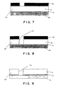
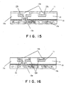
- Figs. 7 to 16 are view for subsequent explanation of the sectional changes of a semiconductor wafer in case of applying the plating method and the plating device of the invention to a practical damascene process. Note that elements in common with the respective figures are indicated with the same reference numerals respectively and their overlapping descriptions are eliminated.
- Figs. 1 and 2 show a plating device 100 respectively.
- the plating device 100 includes an object 10 to be plated, an electrode 12a connected to the object 10, an electrode plate 20 arranged to oppose the object 10, a cell 30 which is filled with a solution containing metal ions essential to this plating process and into which the object 10 and the electrode plate 20 are dipped, a direct-current source 40, a switch 50 for changing the direction of current and a control unit 60 for controlling the operation of the switch 50.
- the plating device 100 is applicable to the damascene process, the object 10 to be processed is not limited to a semiconductor wafer only. We describe the application of the plating device 100 to the damascene process below.
- the object 10 to be processed is identical to the semiconductor wafer and has an insulating film 14, such as SiO 2 , SiOF, and a wiring metal 16.
- the electrode 12a which is used for the formation of a plating film (i.e. an eduction membrane of the metal 16), the removal of a superfluous plating film and the measurement of a thickness of the plating film formed on a wafer surface A.
- the metal 16 is excessively applied on the insulating film 14 having a desired wiring pattern formed thereon.
- the "needed" amount of the metal 16 is equal to an amount necessary and sufficient to fill the contact hole formed in the insulating film 14.
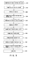
- Fig. 5 is a flow chart of the treatment applied on the object 10 to be processed.
- Figs. 7 to 13 are views showing the sections of the object at the respective steps of Fig. 5.
- Figs. 1 and 2 are views for principled explanation of the plating method and the plating device in principle and therefore, the configurations of the object 10 and the contact hole 15 are different from the same of the objects 10a to 10c shown in Figs. 7 to 16.
- a resist 18a is firstly formed on a wafer 10a, for forming a desired bier thereon (step 1002).
- a photo-resist composed of photosensitive resin is pasted on the wafer having a metal layer 16a, a SiN layer 19 and the insulating film 14.
- a well-known masking unit in this field is used to expose the resist 18a optically.
- the insulating film 14 for example, SiO 2 is employed.
- the metal layer 16a there may be employed a chemical element, such as Cu, Au, Pt.
- the SiN film 19 is added to prevent the exposure of Cu in view of the prevention of Cu from being oxidized in the later-described ashing process using oxygen.
- a mask for example, a hard mask patterned with chromium or chromium-oxide is used. Either contact exposure or projection exposure will do as the optical alignment. Since the development of an exposed photo-resist allows an exposed or non-exposed area to dissolve in a developer, the resist layer in the exposed or non-exposed area is removed to form the resist 18a, as shown in Fig. 7. Note that the pattern formation is well-known as the lithography in this field and therefore the detailed description is eliminated.
- the dry etching using the resist 18a of Fig. 7 is carried out to form a bier 15a in the insulating film 14 (step 1004).
- the resist 18a functions as a protective film (mask) for covering an area where no dry etching is desired.
- the insulating film 14 is etched up to the SiN film 19 by e.g. anisotropic etching.
- the resist 18a and SiN on the metal layer 16a are removed from the wafer 10b having the bier 15a (step 1006).
- the removal of the resist 18a is completed by means of ashing as one dry-etching technique.
- the resist 18a is removed by making used of oxygen radicals.
- a plasma device or an ozone-dissolving device is used for a generator of oxygen radicals.
- the resist 18a includes carbon, hydrogen and oxygen as constituents, the contact with remarkably-reactive oxygen radicals generated by the above device allows the resist 18a to be removed as carbon dioxide and water vapor.
- a resist pattern for establishing a desired wiring line is formed on the wafer 10b (step 1008).
- step 1008 it is executed similarly to step 1002 to form a resist 18b for the desired wiling line.
- the dry etching is carried out while using the resist 18b of Fig. 10 thereby to form a wiring line 15b on the insulating film 14 (step 1010).
- the resist 18b functions as the protective film (mask) for covering an area where no dry etching is desired.
- the process at step 1010 is executed as similar to that at step 1004. Consequently, the insulating film 14 is provided with the bier 15a and the wiring line 15b shown in Fig. 10. In building the wiring line 15b, it is necessary to remove the insulating film 14 so as not to break the configuration of the bier 15a.
- the resist 18b is removed from the wafer 10c having the wiring line 15b (step 1012).
- the removal of the resist 18b is also completed by means of the ashing as one dry-etching technique.
- the process at step 1012 is carried out similarly to that at step 1006.
- the metal 16b is embedded in the bier 15a and the wiring line 15b: nevertheless, as shown in Fig. 12, it is an option before the embedding of metal to form a barrier metal layer 11 for preventing the metal 16b from diffusing into the insulating film 14 and the lower metal layer 16a (step 1014).
- Materials in the TiN-family or the same in the Ta-family represented by tantalum nitride may be employed for the barrier metal layer 11. Note that the formation of the barrier layer 11 can be accomplished by using any method known in this field and therefore the detailed explanation is eliminated.
- a seed layer is formed on the barrier metal layer 11 (step 1016).
- Figs. 5 and 14 it is executed in the metal plating to embed the metal 16b into the bier 15a and the wiring line 15b in the wafer 10c (step 1018).
- the wafer 10c of Fig. 14 corresponds to the object 10 shown in Fig. 1.
- the metal 16b is excessively piled up over the surface of the wafer 10c (i.e. a surface A of the object 10 of Fig. 1).
- the methods of embedding the metal 16b are divided broadly into a dry film deposition method and a wet film deposition method.
- CVD chemical vapor deposition
- PVD plasma vapor deposition
- it is executed for the occurrence of a chemical reaction in the vapor phase or on the surface of the wafer 10c to supply the wafer 10c with gas composed of elements constituting a thin film material, thereby forming a desired thin film.
- plating methods i.e. electrolytic plating and non-electrolytic plating
- the object to be processed shown in Fig. 14 is produced by the electrolytic plating method adopting the plating device 100 of Fig. 1 in the following embodiment.
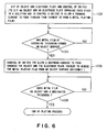
- Fig. 6 is a control flow chart used for the execution of the plating process of Fig. 1 and the later-mentioned plating process of Fig. 2.
- Cu copper
- the electrolytic plating method means dipping the object in the solution containing the objective metal ions thereby to provide an electrode cathode causing the deoxidization, while allowing the forward current to flow between the above cathode and a soluble or insoluble anode (i.e. electrode causing the oxidization), thereby forming an objective metal film on the surface of the object, as an electrolytic educt.
- this technique employs the backward current in order to form the object 10 of Fig. 1 (in detail, before forming the object 10 of Fig. 1), while the backward current is used after forming the object 10 of Fig. 1, in the plating method of the present invention described with reference to Fig. 2 later.
- the electrolytic plating method can be embodied by the plating device 100 of Fig. 1.
- a solution for example, a copper sulfate solution (i.e. the cell 30).
- the electrode 12a is coupled on the object 12a to provide the cathode (negative pole) in opposition to the anode (positive pole) of the electrode plate 20.
- the control unit 60 controls the switch 50 so as to allow the objective metal film 16 to educe on the object 10 in the electrolytic eduction (step 1102).
- the electrode 12a may be formed in CVD, PVD or the other method.
- Fig. 1 is an explanatory diagram in case of providing the electrode 12a on a part of the object to be processed, practically as shown in Fig. 13, the seed layer 12c of metal is formed so as to have a sufficient thickness allowing the electricity through the whole surface of the object, by PVD, CVD or the other method. In this way, it is possible to form the seed layer 12c as the electrode on the barrier metal layer 11 throughout the whole surface of the object.
- the barrier metal layer 11 of Fig. 12 it may be used in place of the electrode 12a. That is, this modification allows the electricity to flow through the barrier metal layer 11.
- the electrode 12a may be replaced by the electrode 12b as shown in Fig.
- Fig. 17 is a schematic view of the plating device 100 having the electrode 12b in a different position.
- the electrode 12b is attached on the bottom of the object 10, so that the current value flowing through the object 10 is transmitted to the control unit 60.
- the electrode 12b is utilized for both formation and removal of the plating film. Additionally, the electrode 12b may be used in order to measure the thickness of the plating film.
- the electrode plate 20 serves as a positive pole thereby to cause the oxidation.
- the material Cu for the positive pole.
- the positive pole there is caused a reaction that each Cu-atom in the Cu-electrode dissolves while discharging two electrons and turns into Cu 2+ consequently.
- the cell 30 is filled up with a solution (plating liquid) containing the objective metal to be plated.
- a solution containing the objective metal to be plated.
- copper sulfate solution of the embodiment copper sulfate is ionized into respective ions of Cu 2+ and SO 4 2- in the solution.
- the ion Cu 2+ is deoxidized by the negative pole thereby to form Cu as the educt.
- the component of Cu forms the objective metal, while the component of sulfuric acid has an action to enhance the electrical conductivity of the solution thereby improving the capability of uniform electro-deposition.
- the plating liquid further contains chlorine and an additive.
- the component chlorine of a designated amount serves as an agent to accelerate both glossiness and dissolution of the positive pole, while the additive has functions to fine the crystal of Cu-atoms as an educt, improve the capability of uniform and reduce an internal stress in the object.
- the other plating liquids there are various solutions having Ni + , Fe + , or the like.
- the direct-current source 40 is equipped with a positive pole and a negative pole.
- the electrode plate 20 forms the positive pole causing the oxidation
- the object 10 to be processed forms the negative pole causing the deoxidization.
- the positive pole of the source 40 is connected to the electrode plate 20, while the negative pole is connected to the object 10.
- the deoxidization from the ions Cu 2+ to the Cu-atoms is performed on the negative pole, while the oxidation from the Cu-atoms to the ions Cu 2+ is performed on the positive pole. Therefore, at the negative pole, the surface of the object 10 is coated with a plating film of the Cu-atoms.
- the plating device is capable of reversing the polarity of the object 10 and the electrode plate 20 freely.
- the operation of the switch 50 is controlled so as to establish the above-mentioned polarity of the object 10 and the electrode plate 20, by the control unit 60.
- the deoxidization is produced on the surface of the object 10 forming the negative pole (the side opposing the electrode plate), so that the ionized copper (Cu 2+ ) acts with two electrons (e - ) generated from the negative pole.
- single- Cu is educed to plate the surface of the object 10 with copper.
- the metal film 16 is substantially flat on its upper surface 17. Because, if the upper surface 17 is so flattened, the metal film 16 could be uniformly removed by the plating process described with reference to Fig. 12 later. As to the planarization of the upper surface 17 of the metal film 16, there have been already proposed a variety of methods in this field. In this embodiment, it is possible to apply any of these methods on the object.
- the control unit 60 is capable of detecting a thickness of the metal film 16 educed on the surface A directly or indirectly by measuring the plating time, the value of plating current, etc.
- detecting the thickness of the metal film 16 by means of the plating time (time passage since the start of plating) and the plating current it is possible to make use of data brought by a previous simulation. In general, it is expected that the smaller film thickness the metal film 16 has, the smaller the current value becomes.
- Such the simulation would be carried out while considering various parameters, for example, concentrations of the metal ions, temperature of the solution, the humidity, etc.
- Fig. 2 is a schematically sectional view of the plating device 100 performing the present plating method.
- the superfluous Cu-film 16 is piled on the surface A.
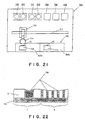
- the CMP method is identical to a method of mechanically flattening the object while using a chemical abrasive, such as slurry, and a polishing pad, the insulating film 14 is also ground inevitably, as described with reference to Fig. 22. Consequently, disadvantageous scratches (tiny cuts), dishing and erosion are produced on the surface A of the insulating film 14, which is far from an ideal flat surface as shown in Fig. 16.
- step 1020 it is executed at the planarization process of Fig. 5 (step 1020) to supply the plating device 100 with the backward current for all or partial removal of the metal film 16b, thereby accomplishing the planarization of the surface A.
- the plating method of Fig. 1 it is difficult to control the plating process so as to educe the metal only in the contact hole 15 of the object 10.
- the inventors of the invention paid attention to a fact that once an excessive amount of metal film 16 is formed on the surface A of the object 10, it is relatively easy to flatten the surface 17 generally. Then, the inventors finally found that, in the plating method of Fig.
- Fig. 4 illustrates a plating film formed on the object 10 by the plating device of Fig. 1.
- Fig. 1 when the switch 50 is controlled so that the control unit 60 allows the backward current to flow between the electrode 12a and the electrode plate 20 (at step 1106 of Fig. 6), the electrode plate 20 turns from the positive pole to the negative pole causing the deoxidization, while the electrode 12a turns from the negative pole to the positive pole causing the oxidation.
- the produced plating film is again dissolved into the solution due to the oxidation from Cu to Cu 2+ , causing the reduction in thickness of the metal film 16 piled up on the surface A.
- the electrode(s) 12a is arranged on left and right sides of the object 10 in Fig. 2 and therefore, it is possible to monitor the current value owing to the existence of film just below the electrode 12a. Since the current value in the object 10 is reduced with the reduction of film thickness, it is possible to control the film thickness by previously calculating a current value flowing at the desired film thickness. Such the control is performed by the control unit 60 connected to e.g. a current meter.
- control unit 60 directly or indirectly judges that the thickness of the metal film 16 on the object 10 reaches the designated thickness (e.g. about 1/10 of a film thickness before switching the direction of current) by current value, time passage and the other parameters (step 1108), it is executed to complete the plating process.
- the designated thickness e.g. about 1/10 of a film thickness before switching the direction of current
- Figs. 18 and 19 show these phenomenons, in which Fig. 18 illustrates the case of a not-patterned tip and Fig. 19 does the case of a patterned tip. Note that, in these experiments, an appropriate current value of 0.14 mA was obtained from the IV curve of the copper sulfate solution on use and thereupon, the plating process was performed with this constant current value.
- the removal of the metal film causes a resistance to be increased abruptly, causing the voltage to be elevated and the current to be reduced radically. Accordingly, it is possible to detect the ending point of the removal of metal film by monitoring both current and voltage or either one of them, whereby the removal process can be controlled by the control unit 60.
- the plating process shown in Fig. 2 (steps 1106 and 1108 of Fig. 6) is substituting for all of the conventional CMP method. Therefore, as a result of such the plating process, it is possible to provide a high-quality semiconductor wafer that does not exhibit the over-polishing at all.
- a CMP device includes a rotary plate, a pad mounted on the rotary plate, means for pressing the object 10 on the rotary plate and means for dropping an abrasive (slurry) onto the pad.
- the CMP method can adopt any technique known in this field, the detailed descriptions about CMP will be eliminated.
- the excessive plating film can be removed by dipping the object 10 into a chemical solvent (i.e. dipping a plated wafer in a solution capable of melting the metal).
- the merit of interrupting the plating process of Fig. 2 may come from a consideration to prevent the metal in the contact hole 15 from dissolving again.
- the application of CMP on the object 10 of Fig. 2 would allow the over-polishing to be remarkably improved in comparison with the application of CMP on the object 10 of Fig. 1 because of its remarkably-reduced quantity to be ground. Consequently, it is possible to provide the semiconductor wafer with high quality in comparison with the case of applying CMP on the object of Fig. 1.
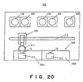
- Fig. 20 is a schematic view of a plating system 200 having the plating devices 100.
- the plating system 200 includes a transfer device 202 for carrying the semiconductor wafer 10 and transporting it to a predetermined position, the plating devices 100 capable of each forming a Cu-plating film on the surface of the wafer 10 and also eliminating the film therefrom, cleaning devices 204 for each washing the wafer 10 having the plating film formed thereon, and a spin drier 206 as a drying device for drying the cleaned wafer 10.
- the plating devices 100 and the cleaning device 204 in two pairs and the only spin drier 206, all of which are arranged in a line.
- the plating system may be provided with three plating devices 100 and two cleaning devices 204. That is, the plating device 100 is not always provided in combination with the cleaning device 204. The number of these devices changes in accordance with a plating condition required for the object.
- the plating system 200 further includes a cassette station 208 equipped with a loading port 208a and an unloading port 208b for the wafers 10.
- a cassette station 208 equipped with a loading port 208a and an unloading port 208b for the wafers 10.
- cassettes 210 each having a plurality of wafers 10, for example, twenty-five wafers.
- Laid between a group of the plating devices 100, the cleaning devices 204 and the spin drier 206 and the cassette station 208 is a rail 212 on which the transfer device 202 is arranged with a transfer arm 214.
- the transfer device 202 In operation, first move the transfer device 202 to the front of the cassette 210 accommodated in the loading port 208a of the cassette station 208 and absorb the wafer 10 in the cassette 210 by an absorbing mechanism of the transfer arm 214. Next, the transfer device 202 moves to the front of the plating device 100 while carrying the wafer 10 and subsequently accommodates it in the plating device 100. After completing to form the plating film on the wafer 10 as mentioned above, the wafer 10 is absorbed by the transfer arm 214 and transported to the interior of the cleaning device 204. Further, the cleaned wafer 10 after removing the plating liquid is again absorbed and reversed by the transfer arm 214 and transported to the interior of the spin drier 206.
- the wafer 10 dried in the spin drier 206 is again absorbed by the transfer arm 214 and transported to the front of the cassette 210 accommodated in the loading port 208b of the cassette station 208 spin drier 206. In this way, the wafer 10 is finally accommodated in the cassette 210.
- the spin drier 206 is arranged independently of the cleaning devices 204, the present invention is not limited to this structure and therefore, they may be replaced with a cleaning and drying device 252 for cleaning and drying the object.
- a cleaning and drying device 252 for cleaning and drying the object.
- the plating system 250 has the cleaning and drying devices 252 in place of the cleaning device 204 and the spin drier 206 besides the plating devices 210.
- the plating system 250 further includes a device 254 having a function to calculate and measure the film thickness of the plating film, a barrier metal etching bath 256 having a function to detect the ending point of the barrier metal etching, and an annealing device 258 for annealing the object, accomplishing the designated treatment more effectively.
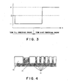
- the negative current of Fig. 3 has a constant current value, it may be replaced by a pulse current whose value is variable within the range of negative values. The same thing can be said of the positive current of Fig. 3.
- the plating device 100 shown in Fig. 1 or 2 employs the copper sulfate solution as an electrolytic liquid, there is no need to limit the electrolytic liquid to the copper sulfate solution.
- a solution containing phosphorus acid may be used and furthermore, it may be replaced with a solution containing any one of acetic acid, nitric acid and hydrochloric acid.
- any one of copper sulfate solution, phosphorus acid solution, acetic acid solution, nitric acid solution and hydrochloric acid solution as the electrolytic liquid, upon storing appropriate current values, which could be obtained from respective IV curves corresponding to the respective electrolytic liquids, in a data base, it may be carried out to read one current value corresponding to the electrolytic liquid on use, out of the data base. If done as above, the treatment could be performed at the current value corresponding to the electrolytic liquid on use. Further, the monitoring of respective values of voltage and current continuously would allow the ending point in removing the plating film to be detected with ease.
- the forward current may be supplied to the first plating device to form the plating film on the object on condition of supplying the backward current to the second plating device in order to remove the plating film.
- it may be executed to differentiate the electrolytic liquids used in the first plating device and the second plating device, from each other.
- the first plating device may employ the copper sulfate solution
- the second plating device may employ the electrolytic liquid containing the phosphorus acid.
- this method of removing part of the metal film formed on the object 10 by the supply of backward current to the object 10 and the electrode plate 20, is also applicable to a case of removing the barrier metal layer 11. Further in the plating system 200 of Fig. 16, it may be equipped with an etching bath for processing the barrier metal.
- the plating method and device of the invention since the use of backward current allows the superfluous metal film to be removed without damaging on the surface of the object, it is possible to reduce or eliminate the possibility of over-polishing derived from grinding, thereby providing the plating treatment of high quality.
Landscapes
- Chemical & Material Sciences (AREA)
- Organic Chemistry (AREA)
- Chemical Kinetics & Catalysis (AREA)
- Electrochemistry (AREA)
- Materials Engineering (AREA)
- Metallurgy (AREA)
- Engineering & Computer Science (AREA)
- Sustainable Development (AREA)
- Life Sciences & Earth Sciences (AREA)
- Internal Circuitry In Semiconductor Integrated Circuit Devices (AREA)
- Electrodes Of Semiconductors (AREA)
- Electroplating Methods And Accessories (AREA)
- Electrical Discharge Machining, Electrochemical Machining, And Combined Machining (AREA)
- Manufacturing Of Printed Wiring (AREA)
- Superconductors And Manufacturing Methods Therefor (AREA)
Abstract
Description
Claims (20)
- A plating method comprising the steps of:dipping an object to be processed and an electrode plate into a solution containing designated metal ions;allowing a forward current to flow through the object and the electrode thereby to form a metal film originated from the designated metal ions on the object; andallowing a backward current to flow through the object and the electrode thereby to remove a part of the metal film formed on the object.
- A plating method comprising the steps of:forming a superfluous amount of metal film on an object to be processed;dipping the object and an electrode plate into a solution containing metal ions as a base of the metal film; andallowing a designated backward current to flow through the object and the electrode thereby to remove a part of the metal film formed on the object.
- A plating method as claimed in Claim 1, wherein the forward current is an electrical current having its variable magnitude.
- A plating method as claimed in Claim 1, wherein the backward current is an electrical current having its variable magnitude.
- A plating method as claimed in Claim 1, further comprising the steps of:measuring the forward current;calculating a thickness of the metal film on the object by the forward current measured; andjudging whether the thickness of the metal film is in excess of a designated thickness; whereinthe removing step is initiated when it is judged at the judging step that the thickness of the metal film is in excess of the designated thickness.
- A plating method as claimed in any one of Claims 1, wherein the metal is identical to copper and the object to be processed is a semiconductor wafer having contact holes.
- A plating method as claimed in any one of Claims 1 to 6, wherein the solution containing the metal ions is a solution containing at least sulfuric acid.
- A plating method as claimed in any one of Claims 1 to 6, wherein the solution containing the metal ions is a solution containing at least phosphoric acid.
- A plating method as claimed in any one of Claims 1 to 6, wherein the solution containing the metal ions is a solution containing at least acetic acid.
- A plating method as claimed in any one of Claims 1 to 6, wherein the solution containing the metal ions is a solution containing at least nitric acid.
- A plating method as claimed in any one of Claims 1 to 6, wherein the solution containing the metal ions is a solution containing at least hydrochloric acid.
- A plating method as claimed in Claim 6, wherein the metal film formed on the object is removed to have one tenth of the thickness at the removing step, and
the plating method further comprises the step of secondly removing a superfluous metal film on the object by executing a chemical mechanical polishing after finishing the removing step. - A plating method as claimed in any one of Claims 1, further comprising the step of forming a barrier metal layer on the object to be processed.
- A plating method as claimed in Claim 13, further comprising the step of forming a seed layer on the object to be processed.
- A plating method as claimed in Claim 13, further comprising the step of allowing the backward current to flow through the object and the electrode plate thereby to remove a part of the barrier metal layer formed on the object.
- A plating device for plating an object to be processed, comprising:a cell allowing the object and an electrode plate to be dipped therein, the cell being capable of accommodating a solution containing designated metal ions for plating;a switch for connecting the object and the electrode plate to a desired polarity of a power source of direct current; anda control unit for controlling the switch in a manner that a forward current flows through the object and the electrode in case of forming a metal film originated from the designated metal ions on the object, while a backward current flows through the object and the electrode in case of removing a surplus of the metal film formed on the object.
- A plating system comprising:a transporting device for transporting an object to be processed;a plating device for applying a plating process on the object; anda cleaning device for washing and cleaning the object subjected to the plating process; whereinthe plating device includes:a cell allowing the object and an electrode plate to be dipped therein, the cell being capable of accommodating a solution containing designated metal ions for plating;a switch for connecting the object and the electrode plate to a desired polarity of a power source of direct current; anda control unit for controlling the switch in a manner that a forward current flows through the object and the electrode in case of forming a metal film originated from the designated metal ions on the object, while a backward current flows through the object and the electrode in case of removing a surplus of the metal film formed on the object.
- A plating system as claimed in Claim 17, further comprising a barrier metal etching bath for removing the barrier metal layer from the object.
- A plating system as claimed in Claim 17, further comprising a device having a function to measure a film thickness of a plating layer.
- A plating system as claimed in any one of Claims 17 to 19, further comprising an annealing device for performing an annealing process.
Applications Claiming Priority (3)
| Application Number | Priority Date | Filing Date | Title |
|---|---|---|---|
| JP21019399 | 1999-07-26 | ||
| JP21019399 | 1999-07-26 | ||
| PCT/JP2000/004988 WO2001007687A1 (en) | 1999-07-26 | 2000-07-26 | Plating method and device, and plating system |
Publications (3)
| Publication Number | Publication Date |
|---|---|
| EP1231300A1 true EP1231300A1 (en) | 2002-08-14 |
| EP1231300A4 EP1231300A4 (en) | 2005-01-26 |
| EP1231300B1 EP1231300B1 (en) | 2007-02-07 |
Family
ID=16585334
Family Applications (1)
| Application Number | Title | Priority Date | Filing Date |
|---|---|---|---|
| EP00949906A Expired - Lifetime EP1231300B1 (en) | 1999-07-26 | 2000-07-26 | Plating method and device, and plating system |
Country Status (7)
| Country | Link |
|---|---|
| US (1) | US6607650B1 (en) |
| EP (1) | EP1231300B1 (en) |
| KR (1) | KR100705371B1 (en) |
| AT (1) | ATE353377T1 (en) |
| DE (1) | DE60033314T2 (en) |
| TW (1) | TW466729B (en) |
| WO (1) | WO2001007687A1 (en) |
Families Citing this family (9)
| Publication number | Priority date | Publication date | Assignee | Title |
|---|---|---|---|---|
| JP2002093761A (en) * | 2000-09-19 | 2002-03-29 | Sony Corp | Polishing method, polishing apparatus, plating method and plating apparatus |
| JP4678720B2 (en) * | 2005-05-31 | 2011-04-27 | 三洋電機株式会社 | Circuit board and manufacturing method thereof, semiconductor device and manufacturing method thereof |
| TWI320606B (en) * | 2006-08-07 | 2010-02-11 | Epistar Corp | A method for making a light emitting diode by electroless plating |
| KR200466385Y1 (en) | 2008-07-25 | 2013-04-17 | 주식회사 케이씨텍 | Method and apparatus for wafer plating |
| JP6161863B2 (en) * | 2010-12-28 | 2017-07-12 | 株式会社荏原製作所 | Electroplating method |
| US9328427B2 (en) * | 2012-09-28 | 2016-05-03 | Sunpower Corporation | Edgeless pulse plating and metal cleaning methods for solar cells |
| JP7697761B2 (en) | 2021-10-01 | 2025-06-24 | 住友電工デバイス・イノベーション株式会社 | Semiconductor device manufacturing method |
| JP7848952B2 (en) | 2022-06-21 | 2026-04-21 | 住友電工デバイス・イノベーション株式会社 | Semiconductor device and method for manufacturing a semiconductor device |
| CN116083844B (en) * | 2023-02-10 | 2025-07-04 | 山东微波电真空技术有限公司 | A method and system for preparing an attenuator |
Family Cites Families (20)
| Publication number | Priority date | Publication date | Assignee | Title |
|---|---|---|---|---|
| JPS57141940A (en) | 1981-02-26 | 1982-09-02 | Nec Home Electronics Ltd | Manufacture of semiconductor device |
| US4466864A (en) | 1983-12-16 | 1984-08-21 | At&T Technologies, Inc. | Methods of and apparatus for electroplating preselected surface regions of electrical articles |
| US5024735A (en) | 1989-02-15 | 1991-06-18 | Kadija Igor V | Method and apparatus for manufacturing interconnects with fine lines and spacing |
| US5256565A (en) * | 1989-05-08 | 1993-10-26 | The United States Of America As Represented By The United States Department Of Energy | Electrochemical planarization |
| JPH04187793A (en) * | 1990-11-20 | 1992-07-06 | Fujitsu Ltd | Semiconductor device and its production |
| US5252196A (en) * | 1991-12-05 | 1993-10-12 | Shipley Company Inc. | Copper electroplating solutions and processes |
| JP2952539B2 (en) * | 1992-03-30 | 1999-09-27 | セイコーインスツルメンツ株式会社 | Micro processing equipment |
| US5302278A (en) * | 1993-02-19 | 1994-04-12 | Learonal, Inc. | Cyanide-free plating solutions for monovalent metals |
| JPH06302607A (en) * | 1993-04-13 | 1994-10-28 | Hitachi Ltd | Bump electrode forming method and semiconductor manufacturing apparatus using the same |
| US5567300A (en) * | 1994-09-02 | 1996-10-22 | Ibm Corporation | Electrochemical metal removal technique for planarization of surfaces |
| US5486282A (en) * | 1994-11-30 | 1996-01-23 | Ibm Corporation | Electroetching process for seed layer removal in electrochemical fabrication of wafers |
| JPH09202990A (en) * | 1996-01-24 | 1997-08-05 | Zenken:Kk | Copper plating liquid |
| JPH1187274A (en) * | 1997-09-01 | 1999-03-30 | Ebara Corp | Semiconductor wafer plating equipment |
| JPH1197391A (en) * | 1997-09-16 | 1999-04-09 | Ebara Corp | Method of electroplating semiconductor wafer wiring |
| US6187164B1 (en) * | 1997-09-30 | 2001-02-13 | Symyx Technologies, Inc. | Method for creating and testing a combinatorial array employing individually addressable electrodes |
| JP3501265B2 (en) * | 1997-10-30 | 2004-03-02 | 富士通株式会社 | Method for manufacturing semiconductor device |
| JP3191759B2 (en) | 1998-02-20 | 2001-07-23 | 日本電気株式会社 | Method for manufacturing semiconductor device |
| US6113771A (en) * | 1998-04-21 | 2000-09-05 | Applied Materials, Inc. | Electro deposition chemistry |
| US6056864A (en) * | 1998-10-13 | 2000-05-02 | Advanced Micro Devices, Inc. | Electropolishing copper film to enhance CMP throughput |
| US6440289B1 (en) * | 1999-04-02 | 2002-08-27 | Advanced Micro Devices, Inc. | Method for improving seed layer electroplating for semiconductor |
-
2000
- 2000-07-26 KR KR1020027001085A patent/KR100705371B1/en not_active Expired - Fee Related
- 2000-07-26 TW TW089114938A patent/TW466729B/en not_active IP Right Cessation
- 2000-07-26 EP EP00949906A patent/EP1231300B1/en not_active Expired - Lifetime
- 2000-07-26 DE DE60033314T patent/DE60033314T2/en not_active Expired - Fee Related
- 2000-07-26 AT AT00949906T patent/ATE353377T1/en not_active IP Right Cessation
- 2000-07-26 WO PCT/JP2000/004988 patent/WO2001007687A1/en not_active Ceased
- 2000-09-18 US US09/665,576 patent/US6607650B1/en not_active Expired - Fee Related
Also Published As
| Publication number | Publication date |
|---|---|
| DE60033314T2 (en) | 2007-08-30 |
| DE60033314D1 (en) | 2007-03-22 |
| US6607650B1 (en) | 2003-08-19 |
| WO2001007687A1 (en) | 2001-02-01 |
| EP1231300A4 (en) | 2005-01-26 |
| KR100705371B1 (en) | 2007-04-11 |
| TW466729B (en) | 2001-12-01 |
| KR20020029907A (en) | 2002-04-20 |
| ATE353377T1 (en) | 2007-02-15 |
| EP1231300B1 (en) | 2007-02-07 |
Similar Documents
| Publication | Publication Date | Title |
|---|---|---|
| KR100780257B1 (en) | Polishing method, polishing apparatus, plating method, and plating apparatus | |
| US6447668B1 (en) | Methods and apparatus for end-point detection | |
| US6881664B2 (en) | Process for planarizing upper surface of damascene wiring structure for integrated circuit structures | |
| US6709565B2 (en) | Method and apparatus for uniform electropolishing of damascene ic structures by selective agitation | |
| US6837984B2 (en) | Methods and apparatus for electropolishing metal interconnections on semiconductor devices | |
| JP2893012B2 (en) | Method and apparatus for planarizing a workpiece | |
| KR100419272B1 (en) | Semiconductor device and method for fabricating the same | |
| Contolini et al. | Electrochemical planarization for multilevel metallization | |
| US6720263B2 (en) | Planarization of metal layers on a semiconductor wafer through non-contact de-plating and control with endpoint detection | |
| JP2005515629A (en) | Electrochemical edge and bevel cleaning method and system | |
| US20020115283A1 (en) | Planarization by selective electro-dissolution | |
| US7136173B2 (en) | Method and apparatus for end-point detection | |
| EP1231300B1 (en) | Plating method and device, and plating system | |
| JP2009532578A (en) | Apparatus and method for confinement area planarization | |
| US6555477B1 (en) | Method for preventing Cu CMP corrosion | |
| KR100859899B1 (en) | Electrochemical Method of Polishing Copper Film on Semiconductor Substrate | |
| JP3507678B2 (en) | Polishing slurry, substrate polishing apparatus and substrate polishing method | |
| JP2007194540A (en) | Semiconductor device manufacturing method and polishing apparatus | |
| US20050029106A1 (en) | Reduction of defects in conductive layers during electroplating | |
| US20030168345A1 (en) | In-situ monitor seed for copper plating | |
| JPWO2001007687A1 (en) | Plating method and apparatus, and plating system | |
| JPH11145139A (en) | Method for manufacturing semiconductor device |
Legal Events
| Date | Code | Title | Description |
|---|---|---|---|
| PUAI | Public reference made under article 153(3) epc to a published international application that has entered the european phase |
Free format text: ORIGINAL CODE: 0009012 |
|
| 17P | Request for examination filed |
Effective date: 20020215 |
|
| AK | Designated contracting states |
Kind code of ref document: A1 Designated state(s): AT BE CH CY DE DK ES FI FR GB GR IE IT LI LU MC NL PT SE |
|
| A4 | Supplementary search report drawn up and despatched |
Effective date: 20041210 |
|
| RIC1 | Information provided on ipc code assigned before grant |
Ipc: 7H 01L 21/288 B Ipc: 7C 25D 7/12 A Ipc: 7H 01L 21/768 B |
|
| GRAP | Despatch of communication of intention to grant a patent |
Free format text: ORIGINAL CODE: EPIDOSNIGR1 |
|
| GRAS | Grant fee paid |
Free format text: ORIGINAL CODE: EPIDOSNIGR3 |
|
| GRAA | (expected) grant |
Free format text: ORIGINAL CODE: 0009210 |
|
| AK | Designated contracting states |
Kind code of ref document: B1 Designated state(s): AT BE CH CY DE DK ES FI FR GB GR IE IT LI LU MC NL PT SE |
|
| PG25 | Lapsed in a contracting state [announced via postgrant information from national office to epo] |
Ref country code: FI Free format text: LAPSE BECAUSE OF FAILURE TO SUBMIT A TRANSLATION OF THE DESCRIPTION OR TO PAY THE FEE WITHIN THE PRESCRIBED TIME-LIMIT Effective date: 20070207 Ref country code: LI Free format text: LAPSE BECAUSE OF FAILURE TO SUBMIT A TRANSLATION OF THE DESCRIPTION OR TO PAY THE FEE WITHIN THE PRESCRIBED TIME-LIMIT Effective date: 20070207 Ref country code: CH Free format text: LAPSE BECAUSE OF FAILURE TO SUBMIT A TRANSLATION OF THE DESCRIPTION OR TO PAY THE FEE WITHIN THE PRESCRIBED TIME-LIMIT Effective date: 20070207 Ref country code: AT Free format text: LAPSE BECAUSE OF FAILURE TO SUBMIT A TRANSLATION OF THE DESCRIPTION OR TO PAY THE FEE WITHIN THE PRESCRIBED TIME-LIMIT Effective date: 20070207 Ref country code: DK Free format text: LAPSE BECAUSE OF FAILURE TO SUBMIT A TRANSLATION OF THE DESCRIPTION OR TO PAY THE FEE WITHIN THE PRESCRIBED TIME-LIMIT Effective date: 20070207 |
|
| REG | Reference to a national code |
Ref country code: GB Ref legal event code: FG4D |
|
| REG | Reference to a national code |
Ref country code: CH Ref legal event code: EP |
|
| REG | Reference to a national code |
Ref country code: IE Ref legal event code: FG4D |
|
| REF | Corresponds to: |
Ref document number: 60033314 Country of ref document: DE Date of ref document: 20070322 Kind code of ref document: P |
|
| PG25 | Lapsed in a contracting state [announced via postgrant information from national office to epo] |
Ref country code: SE Free format text: LAPSE BECAUSE OF FAILURE TO SUBMIT A TRANSLATION OF THE DESCRIPTION OR TO PAY THE FEE WITHIN THE PRESCRIBED TIME-LIMIT Effective date: 20070507 |
|
| PG25 | Lapsed in a contracting state [announced via postgrant information from national office to epo] |
Ref country code: ES Free format text: LAPSE BECAUSE OF FAILURE TO SUBMIT A TRANSLATION OF THE DESCRIPTION OR TO PAY THE FEE WITHIN THE PRESCRIBED TIME-LIMIT Effective date: 20070518 |
|
| PG25 | Lapsed in a contracting state [announced via postgrant information from national office to epo] |
Ref country code: PT Free format text: LAPSE BECAUSE OF FAILURE TO SUBMIT A TRANSLATION OF THE DESCRIPTION OR TO PAY THE FEE WITHIN THE PRESCRIBED TIME-LIMIT Effective date: 20070709 |
|
| ET | Fr: translation filed | ||
| REG | Reference to a national code |
Ref country code: CH Ref legal event code: PL |
|
| PLBE | No opposition filed within time limit |
Free format text: ORIGINAL CODE: 0009261 |
|
| STAA | Information on the status of an ep patent application or granted ep patent |
Free format text: STATUS: NO OPPOSITION FILED WITHIN TIME LIMIT |
|
| 26N | No opposition filed |
Effective date: 20071108 |
|
| GBPC | Gb: european patent ceased through non-payment of renewal fee |
Effective date: 20070726 |
|
| PG25 | Lapsed in a contracting state [announced via postgrant information from national office to epo] |
Ref country code: GR Free format text: LAPSE BECAUSE OF FAILURE TO SUBMIT A TRANSLATION OF THE DESCRIPTION OR TO PAY THE FEE WITHIN THE PRESCRIBED TIME-LIMIT Effective date: 20070508 Ref country code: MC Free format text: LAPSE BECAUSE OF NON-PAYMENT OF DUE FEES Effective date: 20070731 |
|
| PG25 | Lapsed in a contracting state [announced via postgrant information from national office to epo] |
Ref country code: GB Free format text: LAPSE BECAUSE OF NON-PAYMENT OF DUE FEES Effective date: 20070726 |
|
| PG25 | Lapsed in a contracting state [announced via postgrant information from national office to epo] |
Ref country code: IE Free format text: LAPSE BECAUSE OF NON-PAYMENT OF DUE FEES Effective date: 20070726 |
|
| PG25 | Lapsed in a contracting state [announced via postgrant information from national office to epo] |
Ref country code: CY Free format text: LAPSE BECAUSE OF FAILURE TO SUBMIT A TRANSLATION OF THE DESCRIPTION OR TO PAY THE FEE WITHIN THE PRESCRIBED TIME-LIMIT Effective date: 20070207 |
|
| PG25 | Lapsed in a contracting state [announced via postgrant information from national office to epo] |
Ref country code: LU Free format text: LAPSE BECAUSE OF NON-PAYMENT OF DUE FEES Effective date: 20070726 |
|
| PGFP | Annual fee paid to national office [announced via postgrant information from national office to epo] |
Ref country code: BE Payment date: 20090619 Year of fee payment: 10 |
|
| PGFP | Annual fee paid to national office [announced via postgrant information from national office to epo] |
Ref country code: FR Payment date: 20090710 Year of fee payment: 10 |
|
| PGFP | Annual fee paid to national office [announced via postgrant information from national office to epo] |
Ref country code: DE Payment date: 20090723 Year of fee payment: 10 Ref country code: NL Payment date: 20090715 Year of fee payment: 10 |
|
| PGFP | Annual fee paid to national office [announced via postgrant information from national office to epo] |
Ref country code: IT Payment date: 20090725 Year of fee payment: 10 |
|
| BERE | Be: lapsed |
Owner name: TOKYO ELECTRON LTD Effective date: 20100731 |
|
| REG | Reference to a national code |
Ref country code: NL Ref legal event code: V1 Effective date: 20110201 |
|
| REG | Reference to a national code |
Ref country code: FR Ref legal event code: ST Effective date: 20110331 |
|
| PG25 | Lapsed in a contracting state [announced via postgrant information from national office to epo] |
Ref country code: DE Free format text: LAPSE BECAUSE OF NON-PAYMENT OF DUE FEES Effective date: 20110201 |
|
| REG | Reference to a national code |
Ref country code: DE Ref legal event code: R119 Ref document number: 60033314 Country of ref document: DE Effective date: 20110201 |
|
| PG25 | Lapsed in a contracting state [announced via postgrant information from national office to epo] |
Ref country code: NL Free format text: LAPSE BECAUSE OF NON-PAYMENT OF DUE FEES Effective date: 20110201 Ref country code: FR Free format text: LAPSE BECAUSE OF NON-PAYMENT OF DUE FEES Effective date: 20100802 Ref country code: IT Free format text: LAPSE BECAUSE OF NON-PAYMENT OF DUE FEES Effective date: 20100726 |
|
| PG25 | Lapsed in a contracting state [announced via postgrant information from national office to epo] |
Ref country code: BE Free format text: LAPSE BECAUSE OF NON-PAYMENT OF DUE FEES Effective date: 20100731 |