Technical Field
-
The present invention relates to a hot plate for a
semiconductor producing/examining device mainly used in the
semiconductor industry.
Background Art
-
In a semiconductor production/examining device and the
like such as a device for etching and a device for CVD, there
has conventionally been used a heater, a wafer prober and the
like in which a base material made of metal such as stainless
steel, aluminum alloy is used.
-
However, such a conventional heater made of metal as
describe above has following defects.
-
First, the plate thickness of such a heater made of metal
must be relatively large (15 mm or so) , because a metal plate,
if the plate thickness thereof is not large enough, generates
warp, strain and the like due to the thermal expansion caused
by heating, thereby causing breakage or tilting of a silicon
wafer set on the metal plate. When the heater plate is made
too thick, however, the heater becomes too heavy and bulky, which
is also problematic.
-
In a heater made of metal, the temperature of a face on
which an object to be heated such as a silicon wafer is heated
(which face will be referred to as a heating face hereinafter)
is controlled by changing the magnitude of voltage/electric
current applied to a resistance heating element. When the metal
plate as a heater is thick as described above, the temperature
of the heater plate fails to promptly follow the change in the
voltage and/or electric current. In short, temperature
controlling cannot be easily performed in a heater made of metal.
-
In order to overcome such problems as described above,
JP Kokai Hei 11-40330 proposes a ceramic substrate (a hot plate)
in which a nitride ceramic or a carbide ceramic having high heat
conductivity and strength is used as a substrate and a resistance
heating element is provided on a surface of the plate-formed
body made of such a ceramic by baking metal particles on the
substrate surface by sintering.
-
In a hot plate comprising nitride ceramic and the like
as described above, a through hole is generally arranged in a
ceramic substrate thereof and a lifter pin (a pin for supporting
a silicon wafer and the like) is inserted through the through
hole. The object to be heated such as a silicon wafer is supported
by the lifer pin and heated in a state that the object to be
heated is distanced by the length of 50 to 2000 µm from the heating
face of the substrate.
-
When the object to be heated is heated in such manner by
the above-mentioned hot plate, generation of warp, strain and
the like is less likely to happen even at a high temperature
because the hot plate has higher strength due to the use of ceramic,
as compared with a hot plate made of metal. Further, the
above-mentioned hot plate made of nitride ceramic and the like
exhibits relatively excellent temperature following property
to the change of the magnitude of voltage and/or electric current
applied thereto.
-
However, a conventional ceramic substrate made of such
a material exhibits relatively poor sintering property and
relatively low density of the sintered product, and tends to
contain pores therein (refer to JP Kokai Hei 5-8140).
-
In general, a surface of a ceramic substrate is ground
so that the surface is made flat and smooth. However, in the
case of a ceramic substrate having pores therein, a perfectly
flat and smooth surface cannot be formed because the pores inside
the substrate are constantly exposed at the surface even after
the grinding. Thus, significant irregularities exist on the
surface of a conventional ceramic substrate.
-
As a result, when an object to be heated is heated in a
state that the object to be heated is distanced by a certain
distance from the heating face of a substrate, air between the
ceramic substrate and the object to be heated cannot flow as
laminar flow in a stable manner at a constant rate but the air
is divided into a plurality of portions in accordance with the
pattern of the respective portion at which concave portions are
formed at the ceramic substrate, whereby stagnation occurs in
the each portions at which the concave portion is formed.
-
Further, since the distance between the object to be heated
and heating face varies due to the above-mentioned reason, the
quantity of heat reaching the object to be heated also varies
depending on the portion, whereby the temperature distribution
on the heating face is not directly reflected in the object to
be heated. In short, in a conventional ceramic substrate, due
to the reason as described above, the even distribution of
temperature at the object to be heated is not achieved in a
satisfactory manner.
Summary of the Invention
-
The inventors of the present invention have discovered,
as a result of a keen study for solving the above-mentioned
problems, that incorporating oxygen in the ceramic which
constitutes the substrate improves the sintering property of
ceramic, whereby pores at a heating face of a hot plate can be
substantially eliminated or at least the diameter of the pore
can be significantly reduced. The inventors of the present
invention have also discovered that such improvement of the
sintering property realizes a dense structure of the ceramic
substrate, in which grains are bound to each other by a strong
binding force, whereby grains are prevented from falling off
at the time of grinding and thus the glossiness of the heating
face can be enhanced. The present invention has been completed
on the basis of the aforementioned discoveries.
-
Specifically, the present invention provides a hot plate
for a semiconductor producing/examining device, comprising a
resistance heating element formed on a surface of a ceramic
substrate or inside the ceramic substrate, wherein the glossiness
of the heating face of above-mentioned ceramic substrate is 1.5 %
or more.
-
In the present invention, the above-mentioned ceramic
substrate preferably comprises a non-oxide type ceramic which
contains oxygen. This is because, by incorporating oxygen into
a non-oxide type ceramic, the sintering property of the ceramic
substrate is improved, whereby the glossiness thereof can be
enhanced by the grinding process.
-
Further, the above-mentioned ceramic substrate
preferably contains 0.5 to 10 weight % of oxygen. This is because,
when the above-mentioned ceramic substrate contains 0.5 to 10
weight % of oxygen, the sintering property of the ceramic
substrate is improved, whereby the glossiness of the ceramic
substrate can be enhanced by the grinding process.
-
Yet further, the above-mentioned ceramic substrate is
preferably subjected to an annealing treatment. This is because
the shape of grains present on the surface of the ceramic substrate
can be made round by effecting the annealing treatment to the
ceramic substrate, whereby the glossiness of the above-mentioned
ceramic substrate can be enhanced.
-
Yet further, the above-mentioned ceramic substrate is
preferably subjected to the cold isostatic pressing process
before it is sintered. This is because, pores can be completely
eliminated from the formed body which has not been sintered yet
by carrying out the cold isostatic pressing, whereby the
glossiness of the ceramic substrate can be enhanced.
Brief Description of Drawings
-
- Fig. 1 is a bottom view which schematically shows one
example of a hot plate for a semiconductor producing/examining
device of the present invention, in which hot plate a resistance
heating element is formed on the bottom face thereof.
- Fig. 2 is a partially-enlarged sectional view which
schematically shows a portion of the hot plate for a semiconductor
producing/examining device of Fig. 1.
- Fig. 3 is a sectional view which schematically shows a
supporting case in which the hot plate for a semiconductor
producing/examining device of Fig. 1 is arranged.
- Fig. 4 is a partially-enlarged sectional view which
schematically shows one example of a hot plate for a semiconductor
producing/examining device of the present invention, in which
hot plate a resistance heating element is formed inside of the
hot plate.
- Figs. 5(a) to 5(d) are sectional views which schematically
show a part of the process of manufacturing a hot plate for a
semiconductor producing/examining device of the present
invention, in which hot plate a resistance heating element is
formed on the bottom face thereof.
- Figs. 6 (a) to 6 (d) are sectional views which schematically
show a part of the process of manufacturing a hot plate for a
semiconductor producing/examining device of the present
invention, in which hot plate a resistance heating element is
formed inside of the hot plate.
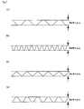
- Figs. 7(a) and 7(b) are explanatory views which explain
the relationship between the glossiness and the average surface
roughness Ra of the ceramic substrate. Figs. 7(c) and 7(d) are
explanatory views which explain the relationship between the
glossiness and the state of the surface of the ceramic substrate.
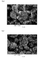
- Fig. 8 is a SEM (scanning electron microscope) photo of
the surface of the ceramic substrate prior to the annealing
treatment.
- Fig. 9 is a SEM photo of the surface of the ceramic substrate
after the annealing treatment.
-
Explanation of numerals
-
- 9
- Silicon wafer
- 10 , 20
- Hot plate
- 11, 21
- Ceramic substrate
- 12, 22
- Resistance heating element
- 13, 23
- External terminal
- 14, 24
- Bottomed hole
- 15, 25
- Through hole
- 16
- Lifter pin
- 18
- Thermocouple
- 27
- Blind hole
- 28
- Conductor-filled through hole
- 30
- Supporting case
- 30a
- Coolant outlet
- 32
- Guide pipe
- 35
- Heat insulator
- 37
- Metal member for pressing
- 38
- Bolt
- 39
- Coolant inlet pipe
- 130
- Solder paste layer
- 170
- Socket
Detailed Description of Invention
-
A hot plate for a semiconductor producing/examining device
of the present invention comprises a resistance heating element
formed on a surface of a ceramic substrate or inside the ceramic
substrate, wherein the glossiness of the heating face of said
ceramic substrate is 1.5 % or more.
-
In the case of the ceramic substrate having such glossiness
as described above, when a silicon wafer is heated in a state
that the silicon wafer is distanced by the length of 50 to 500
µm from the heating face of the hot plate for a semiconductor
producing/examining device (which may be referred to as simply
hot plate hereinafter) , stagnation and the like of air is less
likely to occur between the heating face and the object to be
heated because the heating face is sufficiently flat, whereby
the air flows as laminar flow at a constant flow rate. Further,
as the distance between the object to be heated and the heating
face is substantially constant allover the heating face, it is
prevented that the quantity of heat reaching the heating face
varies depending on the portion of the heating face . As a result,
the object to be heated such as a silicon wafer and the like
can be evenly heated.
-
Yet further, in a case that a silicon wafer is put directly
on the heating face of the ceramic substrate, the contact between
the silicon wafer and the heating face is effected as a perfectly
continuous surface-contact, whereby the obj ect to be heated such
as a silicon wafer can be evenly heated.
-
Japanese Patent gazette No. 2513995 and other references
disclose that it is possible to form a smooth surface having
Ra (surface roughness) of 1 µm or less at the substrate. However,
the Ra of the above-described references is the information of
the depth of the irregularities on the substrate surface and
does not prescribe the density of the irregularities at all.
On the other hand, in the hot plate of the present invention,
the density of the irregularities as well as the depth thereof,
on the substrate surface is controlled, by referring to the
glossiness as an idex, so that the hot plate can evenly heat
the object to be heated.
-
In the present invention, the glossiness includes the
information of not only the depth of the irregularities but also
the density thereof.
-
Figs. 7(a) and 7(b) are explanatory views which explain
the relationship between the glossiness and the average surface
roughness Ra of the ceramic substrate. Figs. 7(c) and 7(d) are
explanatory views which explain the relationship between the
glossiness and the state of the surface of the ceramic substrate .
-
Although Ra as the average surface roughness of the ceramic
substrate is 0.1 µm in both Figs. 7(a) and 7 (b) , the configuration
shown in Fig. 7(a) exhibits a larger glossiness than the
configuration shown in Fig. 7(b). This example demonstrates
that Ra does not reflect the information of the density of the
irregularities on the surface. That is, even when Ra as the
surface roughness is increased, a sufficiently large glossiness
can be expected if the density of the irregularities at the surface
is significantly small.
-
Further, as is explained in Figs. 7(c) and 7(d), the
glossiness of the surface configuration of Fig. 7(c) having sharp
irregularities is different from the glossiness of the surface
configuration of Fig. 7(d) having round irregularities, even
if Ra as the average surface roughness of the ceramic substrate
is 0.1 µm in both Figs. 7(c) and 7(d) and the density of the
irregularities is also the same in the two configurations. In
this case, the glossiness of Fig. 7(d) configuration is higher
than that of Fig. 7(c) configuration. That is, the glossiness
has the information of not only the density of the irregularities
but also the information of the surface state of the roughened
surface.
-
In the case of the inventions described in the
above-mentioned references, in which no specific attempt is made
to incorporate oxygen and the like into the ceramic substrate,
concaved portions resulted from the portions which have not been
sintered which is produced at the grain boundary and/or concaved
portions produced because of particles which have fallen off,
may be generated. If such concaved portions are present as a
cluster at the ceramic surface, it is difficult to achieve the
glossiness of 1.5 % or more even in the case that there exists
no pin hole.
-
The ceramic substrate according to the present invention
exhibits excellent sintering property and has a sufficiently
high density, whereby the diameter of pore present inside the
substrate is significantly small and thus the ceramic substrate
is formed dense as compared with that of the conventional one.
Accordingly, the grains constituting the sintered body are firmly
bound to each other, whereby the particles hardly come off by
grinding and a sufficiently flat and smooth surface can formed.
As a result, the glossiness of the substrate of 1.5 % or more
can be reliably achieved and the free particles are not generated.
-
Here, the glossiness of the ceramic substrate represents
the glossiness measured by the method according to JIS K 7105
5.2 section (the method of testing optical properties of a
plastic). The surface glossiness of ceramic can be measured
by this method on the basis of the same principal, although the
method is proposed for measuring the glossiness of plastic
surface.
-
In the above-mentioned method, light is irradiated on the
sample surface at the incidence angle of 60 ° so that the regular
reflection components are measured by using a photoreceiver.
A glass surface having refractive index of 1.567 is employed
as the reference of the relative-specular glossiness. That is,
the glossiness of the obtained data is evaluated with respect
to glossiness of the above-mentioned reference as 100 %.
-
Examples of the method of enhancing the glossiness include:
a method of eliminating pore of the ceramic substrate and
particles which fall off from the substrate; and a method of
making the irregularities on the surface of the ceramic substrate
round.
-
Examples of the above-mentioned method of eliminatingpore
and particles which fall off include: a method of firing nitride
ceramic or carbide ceramic as the raw material in air, so that
oxygen is introduced into the ceramic and the sintering property
at the grain boundary is improved; a method of completely
eliminating pore, by subjecting the formed body to cold isostatic
pressing prior to the sintering; and the like. Examples of the
method of making the irregularities at the ceramic surface round
include: a method of making the irregularities at the ceramic
surface round and gentle-slope by subjecting the sintered body
to the annealing treatment; and the like.
-
Regarding the above-mentioned annealing treatment, Fig.
8 shows a SEM photograph of the ceramic substrate surface which
has not been subjected to annealing and Fig. 9 shows a SEM
photograph of the ceramic substrate surface which has been
subjected to annealing. The sample of Fig. 9 which has been
subjected to annealing exhibits higher glossiness of the ceramic
substrate. Specifically, the sample shown in Fig. 8 exhibits
glossiness of 1.1 %, while the sample shown in Fig. 9 exhibits
glossiness of 20 %.
-
In the present invention, incorporation of oxygen into
the ceramic contain, for example, results in a dense structure
of the ceramic substrate in which grains thereof are firmly bound
to each other. Accordingly, by subjecting a ceramic substrate
having such a structure to the grinding process, a hot plate
whose glossiness at the ceramic substrate surface is 1.5 % or
more can be realized.
-
Alternatively, the glossiness at the ceramic substrate
surface can be set within the above-mentioned range by a method
including the steps of: making the structure of a ceramic
substrate dense by subjecting the formed body which is not yet
sintered, during the production process thereof, to cold
isostatic pressing (CIP); and then carrying out the sintering
process of the ceramic substrate.
-
The method of incorporating oxygen into a ceramic substrate
will be described later.
-
Further, by firing the above-mentioned ceramic substrate
at 1400 to 1800 °C so that the grains at the above-mentioned
ceramic substrate surface have round configurations, the
irregularities at the ceramic substrate surface can be made
smooth and gentle-slope, whereby the glossiness at the
above-mentioned ceramic substrate surface can be improved.
-
Fig. 1 is a bottom view which schematically shows one
example of a hot plate of the present invention. Fig. 2 is a
partially-enlarged sectional view which schematically shows a
portion of the hot plate of Fig. 1. In the hot plate of Fig.
1, a resistance heating element is formed on the bottom face
of the ceramic substrate.
-
As shown in Fig. 1, the ceramic substrate 11 is formed
so as to have a disc-like shape, and a plurality of resistance
heating elements 12 are formed in a pattern of concentric circles
on the bottom face 11b of the ceramic substrate 11. In the
resistance heating element 12, each set of two concentric circles
close to each other forms one continuous line as one circuit,
and the combination of these circuit sets are designed so that
the temperature distribution on the heating face 11a is made
even.
-
Further, as shown in Fig. 2, a metal covering layer 12a
is provided on each of the resistance heating elements 12, so
that the resistance heating elements are prevented from being
oxidized. An external terminal 13 is connected to each end
portion of the resistance heating element 12 by using solder
and the like (not shown). A socket 170 having wiring is connected
to the external terminal 13, whereby the external terminal 13
is connected to a power source.
-
A bottomed hole 14 in which a temperature measuring element
18 is to be inserted is formed at the ceramic substrate 11. A
temperature measuring element 18 such as a thermocouple and the
like is embedded inside the bottomed hole 14. A through hole
15 through which a lifter pin 16 is to be inserted is formed
at a portion near to the center of the ceramic substrate 11.
-
The lifter pin 16 is designed such that the lifter pin
16 can be moved in the vertical direction with carrying a silicon
wafer 9 put thereon. By moving the lifter pin 16 in the vertical
direction, the silicon wafer 9 can be transferred to a conveyer
(not shown) or the silicon wafer 9 can be received from a conveyer.
In addition, the silicon wafer 9 can be set on the heating face
11a of the ceramic substrate 11 so that the silicon wafer 9 is
heated, or the silicon wafer 9 can be supported in a state that
the silicon wafer 9 is distanced by the length of 50 to 2000
µm from the heating face 11a, so that the silicon wafer 9 can
be heated.
-
Alternatively, it is acceptable that the silicon wafer
9 is heated in a state that the silicon wafer 9 is distanced
by the length of 50 to 2000 µm from the heating face 11a, by:
forming a through hole or a concave portion in the ceramic
substrate 11; inserting a supporting pin having a tip end shaped
in a form of pointing tower or semisphere into the through hole
or the concave portion; fixedly holding the supporting pin in
a state that the supporting pin is slightly projected from the
ceramic substrate 11; and supporting the silicon wafer 9 by the
supporting pin.
-
Fig. 3 is a sectional view which schematically shows a
supporting case in which the ceramic substrate as describe above
which constitutes a hot plate is arranged.
-
In a case that the ceramic substrate 11 is used in a state
that the ceramic substrate 11 has been fitted in a supporting
case as shown in Fig. 3, a guide pipe 32 is provided under the
portion at which the through hole 15 has been formed, of the
ceramic substrate 11, such that the guide pipe 32 communicates
with the through hole 15. A lifter pin 16 is inserted through
the through hole 15, whereby the silicon wafer 9 can be supported
in a state that the silicon wafer 9 is distanced from the surface
of the ceramic substrate 11.
-
Further, a coolant outlet 30a is formed in the supporting
case 30 such that the coolant introduced from a coolant inlet
pipe 39 is discharged outside through a coolant outlet 30a. By
the action of the coolant, the ceramic substrate 11 can be cooled.
-
Accordingly, after activating the hot plate such that the
hot plate 10 is heated and the temperature of the silicon wafer
9 is increased to a predetermined temperature, the ceramic
substrate 11 can then be cooled by introducing the coolant from
the coolant inlet pipe 39.
-
When the silicon wafer 9 is heated as shown in Fig. 3,
by using the hot plate of the present invention whose glossiness
on the heating face thereof is 1.5 % or more, in a state that
the silicon wafer 9 is distanced by a certain distance from the
heating face 11a, the distance between the silicon wafer and
the heating face is substantially constant all over the heating
face because the heating face is excellently flat and smooth,
whereby there exists no portion on the heating face at which
portion air stagnates between the silicon wafer and the heating
face. As a result, the air between the silicon wafer and the
heating face flows as laminar flow and thus the silicon wafer
9 can be evenly heated.
-
Fig. 4 is a partially enlarged sectional view which
schematically shows another example of the hot plate of the
present invention. In the hot plate of Fig. 4, a resistance
heating element is formed inside the ceramic substrate.
-
In the hot plate, a ceramic substrate 21 is formed so as
to have a disc-like shape as is the case with the hot plate shown
in Fig. 1, and a resistance heating element 22 is provided inside
the ceramic substrate 21 in a pattern similar to that shown in
Fig. 1, i.e., in the concentric circles-like pattern in which
each set of two adjacent concentric circles form a set of circuit,
although the structure of the resistance heating element 22 is
not shown by drawings.
-
A conductor-filled through hole 28 is formed right under
the end portion of the resistance heating element 22. A blind
hole 27 is formed on the bottom face 21b of the ceramic substrate
21 such that the conductor-filled through hole 28 is exposed
outside. An external terminal 23 is inserted in the blind hole
27 and connected thereto by using a brazing-filler (not shown)
and the like.
-
Although not shown in Fig. 4, a socket having a conductive
wire, for example, is connected to the external terminal 23 in
a manner similar to that in the hot plate of Fig. 1. The conductive
wire is connected to a power source.
-
In the hot plate shown in Fig. 4, the surface of the heating
face has the glossiness of 1.5 % or more, and is very flat.
Accordingly, the object to be heated such as a silicon wafer
and the like can be evenly heated, by using the hot plate of
Fig. 4, in a manner similar to that of the hot plate shown in
Figs. 1 and 2.
-
The ceramic substrate according to the present invention
preferably comprises at least one type of the ceramic material
selected from the group consisting of nitride ceramic, carbide
ceramic and oxide ceramic.
-
Examples of the nitride ceramic include metal nitride
ceramic such as aluminum nitride, siliconnitride, boronnitride,
titanium nitride and the like.
-
Examples of the carbide ceramic include metal carbide
ceramic such as silicon carbide, zirconium carbide, titanium
carbide, tantalum carbide, tungsten carbide and the like.
-
Examples of the oxide ceramic include metal oxide ceramic
such as alumina, zirconia, cordierite, mullite, MgO, CaO, TiO2
and the like.
-
In the present invention, it is preferable that two or
more types of these oxide ceramics are used in combination. For
example, a mixture of oxides such as alumina, silica, CaO, MgO
and the like is likely to have a dense structure.
-
Among the above-mentioned examples of ceramic, the ceramic
materials which are non-oxide type are preferable, because
non-oxide ceramics have excellently high heat conductivity and
can excellently transfer the heat generated at the resistance
heating element to the object to be heated. As such a non-oxide
ceramic, a nitride ceramic is especially preferable.
-
Among the above-mentioned examples of the nitride ceramic,
the aluminum nitride is the most preferable because the heat
conductivity thereof is the highest (180 W/m K).
-
In a case that the above-mentioned nitride ceramic
incorporates oxygen, the sintering process is facilitated, the
porosity is significantly decreased and the diameter of the
remaining pore is made small, whereby grinding can be more easily
carried out and the glossiness of the surface thereof is enhanced.
-
The ceramic substrate constituting the hot plate of the
present invention contains preferably 0.05 to 10 weight %; or
especially preferably 0.1 to 5 weight % of oxygen. When the
oxygen content in the ceramic substrate is less than 0.1 weight %,
the glossiness of the substrate surface may not be enhanced by
grinding; or a sufficient breakdown voltage may not be obtained,
due to the poor sintering property of the substrate. On the
other hand, when the oxygen content in the ceramic substance
exceeds 5 weight %, the heat conductivity is lowered and the
temperature-rising/dropping property of the substrate may
deteriorate. Further, the above-mentioned ceramic substrate
most preferably contains 0.5 weight % or more of oxygen, this
is because the grains at the ceramic substrate surface can be
easily made round by subjecting the ceramic substrate to
annealing when the content of oxygen in the ceramic substrate
is in this range.
-
Oxygen is introduced to the ceramic substrate by: adding
a sintering aid; or firing a non-oxide ceramic in air or oxygen.
-
In general, a metal oxide is mixed into the raw material
powder of non-oxide ceramic and the mixture is fired so that
oxygen is incorporated into the non-oxide ceramic.
-
When nitride ceramic is used as the above-mentioned
non-oxide ceramic, examples of the metal oxide to be mixed with
the nitride ceramic include an oxide of an alkali metal, an
alkaline earth metal and a rare earth metal. Specific examples
thereof include yttria (Y2O3), alumina (Al2O3), rubidium oxide
(Rb2O), lithium oxide (Li2O), calcium oxide (CaO3) and the like.
-
The preferable content of the metal oxide in the nitride
ceramic is 1 to 10 parts by weight with reference to 100 parts
by weight of the nitride ceramic.
-
The porosity of the above-mentioned ceramic substrate is
preferably 5 % or less.
-
When the porosity exceeds 5 %, the possibility that pores
are exposed on the substrate surface at the time of the grinding
process increases, whereby the flatness of the substrate surface
deteriorates and it is difficult to achieve the surface
glossiness of 1.5 % or more.
-
Accordingly, the porosity is more preferably in a range
of 0.1 to 1.0 % or so.
-
The pore diameter of the above-mentioned ceramic substrate
is preferably 5 µm or less, and more preferably in a range of
0.1 to 3 µm.
-
When the average of the pore diameter exceeds 5 µm, pores
are more likely to be exposed on the substrate surface, whereby
the surface flatness of the substrate deteriorates.
-
The above-mentioned porosity is measured by the
Archimedes' method. This method includes the steps of:
pulverizing the sintered body and putting the pulverized sample
into an organic solvent or mercury, to measure the volume thereof;
obtaining the true specific gravity from the weight of the
pulverized sample and the volume thereof; and calculating the
porosity from the obtained true specific gravity and the apparent
specific gravity.
-
The measurement of the average diameter of pore is
performed by: preparing five samples and grinding the surfaces
thereof into mirror planes; photographing the surface of each
sample at ten sites by an electron microscope with 2000 to 5000
magnification; and obtaining the average of the pore diameters
of the photographed 50 shots. Note that the longest portion
at each pore is measured as the diameter of the pore thereof.
-
The above-mentioned hot plate desirably contains carbon
by the amount of 50 to 5000 ppm. By adding carbon, the ceramic
substrate can be blackened so that the radiation heat can be
fully utilized when the hot plate is used as a heater.
-
The carbon may be amorphous or crystalline. When
amorphous carbon is used, the decrease in the volume resistivity
at a high temperature can be prevented. When the crystalline
carbon is used, the decrease in the heat conductivity at a high
temperature can be prevented. Accordingly, both crystalline
carbon and amorphous carbon may be used depending on the
application. The content of carbon is preferably in a range
of 50 to 2000 ppm.
-
In the hot plate of the present invention, a resistance
heating element is generally provided on the bottom face or inside
the ceramic substrate, and a silicon wafer and the like is heated
by the heat generated by the resistance heating element. However,
the heating or cooling of the ceramic substrate may be carried
out by providing a Peltier device.
-
In a case that the resistance heating element is provided
inside the ceramic substrate, plural layers of the resistance
heating element may be provided therein. In this case, it is
preferable that the patterns at the layers are designed so that
the patterns complement each other. For example, a structure
such as staggered arrangement may be used.
-
Examples of the resistance heating element material
include a sintered body of metal or conductive ceramic, a metal
foil, a metal wire and the like. As the metal sintered body,
at least one type selected from tungsten sintered body and
molybdenum sintered body is preferable, because these metals
are relatively less likely to be oxidized and have a sufficient
resistance value for generating heat.
-
As the conductive ceramic, at least one type selected from
carbides of tungsten and molybdenum may be used.
-
Further, in a case that the resistance heating element
is formed on the bottom face of the ceramic substrate, it is
preferable to use noble metal (gold, silver, palladium, platinum)
or nickel as the metal sintered body. Specifically, silver,
silver-palladium and the like can be preferably used.
-
The shape of the metal particles used for producing the
metal sintered body may be either spherical or scaly.
Alternatively, both spherical particles and scaly particles may
be used in a mixed manner.
-
In the case that the resistance heating element is provided
on the surface, a metal oxide may be added to the metal sintered
body. The metal oxide is used in order to tightly adhere the
metal particles to the ceramic substrate. The reason why the
metal oxide improves the adhesion of the metal particles to the
ceramic substrate is not clearly known. A thin oxidized film
is formed on the surface of the metal particle, and an oxidized
film is also formed on the surface of the ceramic substrate,
regardless of whether the ceramic substrate is oxide ceramic
or non-oxide ceramic. It is thus assumed that the oxidized film
of the metal particle and that of the ceramic substrate are
combined to one film by way of the metal oxide when these oxidized
films are sintered at the surface of the ceramic substrate,
whereby the metal particles tightly adhere to the ceramic
substrate.
-
As the metal oxide, at least one type of compound selected
from the group consisting of lead oxide, zinc oxide, silica,
boron oxide (B2O3), alumina, yttria and titania is preferably
used, because these oxides can improve adhesion of the metal
particles to the ceramic substrate without increasing the
resistance value of the resistance heating element too much.
-
The content of the metal oxide is preferably 0.1 parts
by weight or more and less than 10 parts by weight with reference
to 100 parts by weight of the metal particles. By using the
metal oxide within the aforementioned range, the adhesion between
the metal particles and the ceramic substrate can be enhanced
without increasing the resistance value too much.
-
The contents of lead oxide, zinc oxide, silica, boron oxide
(B2O3), alumina, yttria and titania are preferably 1 to 10 parts
by weight for lead oxide, 1 to 30 parts by weight for silica,
5 to 50 parts by weight for boron oxide, 20 to 70 parts by weight
for zinc oxide, 1 to 10 parts by weight for alumina, 1 to 50
parts by weight for yttria and 10 to 50 parts by weight for titania,
with reference to the whole weight of the metal oxides expressed
as 100 parts by weight. It is preferable that these contents
of the metal oxides are adjusted so that the total sum of the
metal oxides does not exceed 100 parts by weight, because these
metal oxides can especially enhance adhesion thereof to the
ceramic substrate in the above-mentioned range.
-
In a case that the resistance heating element is provided
on the bottom face of the ceramic substrate, the surface of the
resistance heating element 12 is preferably covered with a metal
covering layer 12a (refer to Fig. 2). As the resistance heating
element 12 is a sintered body of metal particles, the resistance
heating element 12 is easily oxidized if it is exposed in the
air, and the resistance value thereof changes due to the
oxidization. By covering the surface of the resistance heating
element 12 with a metal covering layer 12a, such oxidization
can be prevented.
-
The thickness of the metal covering layer 12a is preferably
in a range of 0.1 to 10 µm. When the thickness of the metal
covering layer 12a is within this range, the oxidization of the
resistance heating element can be prevented without changing
the resistance value of the resistance heating element too much.
-
The metal used for the metal covering layer is not
particularly limited, as long as the metal is non-oxidizable.
Specific examples thereof .include at least one type of metal
selected from the group consisting of gold, silver, palladium,
platinum and nickel. Among these examples, nickel is the most
preferable. The resistance heating element requires a terminal
for effecting connection of the resistance heating element to
the power source, and this terminal is attached to the resistance
heating element through solder. Herein, nickel effectively
prevents the heat dissipation due to solder. As the connection
terminal, a terminal pin made of Kovar can be used.
-
In a case that the resistance heating element is formed
inside the ceramic substrate, the surface of the resistance
heating element is not oxidized and thus no covering by the metal
layer is required . When the resistance heating element is formed
inside the ceramic substrate, a portion of the surface of the
resistance heating element may be exposed outside of the heater
plate.
-
Preferable examples of the metal foil used as the
resistance heating element include a resistance heating element
produced by a pattern-forming process such as etching of nickel
foil or stainless foil.
-
The metal foils which have been subjected to the
pattern-forming process may be laminated with a resin film and
the like.
-
Example of the metal wire include a tungsten wire, a
molybdenum wire and the like.
-
In a case that a Peltier device is used as the temperature
controlling means, either heating or cooling can be performed
by the same element by changing the flow direction of the current,
which is advantageous.
-
In the present invention, a thermocouple may be embedded
in the bottomed hole 14 of the ceramic substrate 11, according
to necessity. In such a structure, the temperature of the
resistance heating element can be measured by the thermocouple,
so that the temperature of the resistance heating element can
be controlled by changing the magnitude of the voltage or the
current on the basis of the obtained data.
-
It is preferable that the size of the connecting portion
of the metal wire of the thermocouple is the same as or larger
than the strand diameter of each metal wire, and 0.5 mm or less.
The heat capacity of the connecting portion is made small by
adapting such a structure, whereby the temperature is converted
into the current value correctly and rapidly. As a result, the
temperature controllability is improved and the temperature
distribution on the heating face of the wafer is made small.
-
Examples of the aforementioned thermocouple include the
K-type, the R-type, the B-type, the S-type, the E-type, the J-type
and the T-type thermocouples, as is raised in JIS-C-1602 (1980).
-
Next, the method of producing the hot plate of the present
invention will be described.
-
Figs. 5 (a) to 5(d) are sectional views which schematically
depict the method of producing a hot plate having a resistance
heating element formed on the bottom face of the ceramic substrate
thereof.
(1) Production process of a ceramic substrate
-
The above-mentioned ceramic powder such as aluminum
nitride and the like is blended with a sintering aid comprising
an oxide such as yttria and the like, a binder and the like,
according to necessity, whereby a slurry is prepared. The
prepared slurry is granulated by an appropriate method such as
spray drying. The obtained granules are filled in a mold and
the like and pressed for forming, so that a raw formed body (green)
is produced. Amorphous or crystalline carbon may be added at
the time of slurry preparation as described above.
-
Here, when the raw formed body (green) is produced, it
is preferable that the raw formed body (green) is then subjected
to cold isostatic pressing (CIP) and the like. In a case that
the formed body which has not been sintered is evenly pressed
by cold isostatic pressing and the like, sintering proceeds
evenly and thus the density of the sintered substrate is enhanced,
whereby the glossiness of the surface thereof can be easily
adjusted so as to be 1.5 % or more.
-
The pressure of the above-mentioned cold isostatic
pressing (CIP) is preferably in a range of 50 to 500 MPa.
-
Next, the raw formed body is heated and fired to effect
sintering, whereby a plate-formed body made of ceramic is
produced. Thereafter, a ceramic substrate 11 is produced by
processing the plate-formed body into a predetermined shape.
Alternatively, the plate-formed body may be produced such that
the plate-formed body can be used as the ceramic substrate 11
after firing without any further processing (Fig. 5(a)). A
ceramic substrate 11 having no pore can be produced by conducting
heating and firing with applying a pressure. The temperature
at which heating and firing are to be carried out is not
particularly restricted as long as the temperature is no lower
than the sintering temperature . In the case of nitride ceramic,
the preferable temperature range is 1000 to 2500 °C. In this
case, the firing temperature is more preferably in a range of
1600 to 2100 °C.
-
Next, a through hole through which a supporting pin for
supporting a silicon wafer is inserted, a through hole 15 through
which a lifter pin for transferring a silicon wafer is inserted,
the bottomed hole 14 in which a temperature measuring element
such as a thermocouple is embedded, and the like are optionally
formed in the ceramic substrate 11.
(2) Process for printing a conductor containing paste on the
ceramic substrate
-
A conductor containing paste is generally a fluid substance
having high viscosity, comprising metal particles, a resin and
a solvent. By printing, by screen printing and the like, this
conductor containing paste on a portion of the ceramic substrate
at which portion the resistance heating element is to be provided,
a conductor containing paste layer is formed. As the resistance
heating element is required to heat the ceramic substrate evenly
such that the ceramic substrate as a whole reaches the same
temperature, it ispreferable that the resistance heating element
is printed so as to have a concentric circles-like pattern or
a pattern in which the concentric circles-like pattern and the
winding line-like pattern are combined.
-
It is preferable that the conductor containing paste layer
is formed such that the section of the resistance heating element
12 after sintering has a quadrilateral, flat section.
(3) Firing of the conductor containing paste
-
The conductor containing paste layer printed on the bottom
face of the ceramic substrate 11 is heated and fired, so that
the resin and the solvent are removed and the metal particles
are sintered and baked on the bottom face of the ceramic substrate
11, whereby the resistance heating element 12 is formed (refer
to Fig. 5(b)). The temperature during the heating and firing
process is preferably in a range of 500 to 1000 °C.
-
In a case that the above-mentioned metal oxide is added
to the conductor containing paste, the metal particles, the
ceramic substrate and the metal oxide are sintered and made
integral, whereby adhesion between the resistance heating
element and the ceramic substrate is improved.
-
Thereafter, the surface of the sintered body is ground
by using a surface grinding machine. The surface is further
ground by using a diamond whetstone of #100 to #8000. Next,
the glossiness of the surface of the sintered body is adjusted
by polishing the surface with diamond slurry whose average
particle diameter is 0.1 to 10 µm, colloidal silica or alumina
suspension.
-
Alternatively, the surface of the sintered body may be
subjected to annealing for 1 to 3 hours at the temperature of
1400 to 1800 °C, so that the glossiness of the heating face for
the semiconductor wafer is enhanced.
-
The above-mentioned grinding treatment, polishing
treatment and annealing treatment may be carried out in the
combined manner.
(4) Formation of the metal covering layer
-
Next, a metal covering layer 12a is provided on the surface
of the resistance heating element 12 (Fig. 5(c)). The metal
covering layer 12a can be formed by electrolytic plating,
electroless plating, spattering and the like. Among these
methods, electroless plating is the most preferable in terms
of achieving high productivity.
(5) Attaching of the terminals and the like
-
External terminals 13 for effecting connection to the power
source are attached to the end portions of the circuit of the
resistance heating element 12 through a solder paste layer 130
(refer to Fig. 5(d)). A temperature measuring element 18 such
as a thermocouple and the like is inserted in the bottomed hole
14 and the bottomed hole 14 is sealed by using a heat resistant
resin and the like, such as polyimide. Further, a socket and
the like (not shown) having conductive wires, for example, is
attached to the external terminal 17 in a detachable manner.
(6) Thereafter, the ceramic substrate having the resistance
heating element 12 as described above is fitted to, for example,
a cylindrical supporting case and the lead wire extending from
the socket is connected to the power source, whereby the
production of the hot plate is completed.
-
When the above-mentioned hot plate is produced, an
electrostatic chuck can be produced by providing electrostatic
electrodes inside the ceramic substrate, or a wafer prober can
be produced by providing a chuck top conductor layer on the heating
face and providing a guard electrode and a ground electrode inside
the ceramic substrate.
-
In the case that the electrodes are provided inside the
ceramic substrate, such a structure can be realized by embedding
a metal foil and the like inside the ceramic substrate. In the
case that conductor layer is formed on the surface of the ceramic
substrate, such a process can be carried out by spattering or
plating or by the combination of spattering and plating.
-
Next, a method of producing the hot plate having the
resistance heating element formed inside the ceramic substrate
thereof, according to the present invention, will be described
hereinafter.
-
Figs. 6(a) to 6(d) are sectional views which schematically
depict the method of producing a hot plate having a resistance
heating element formed inside the ceramic substrate thereof.
(1) Process of producing a green sheet
-
First, a paste is prepared by mixing nitride ceramic powder
with a binder, a solvent and the like. A green sheet is then
produced by using the paste.
-
As the above-mentioned ceramic powder, aluminum nitride
and the like can be used. A sintering aid comprising an oxide
such as yttria and the like may optionally be added to the ceramic
powder. When a green sheet is produced, crystalline or amorphous
carbon may be added.
-
As the binder, at least one type of binder selected from
the group consisting of an acrylic binder, ethyl cellulose, butyl
cellosolve and polyvinyl alcohol is preferably used.
-
As the solvent, at least one type of solvent selected from
α-terpineol and glycol is preferably used.
-
The paste obtained by mixing the above-mentioned
components is formed into a sheet-like shape by the doctor blade
method, whereby a green sheet 50 is produced.
-
The thickness of the green sheet 50 is preferably in a
range of 0.1 to 5 mm.
-
Next, a portion which is to serve as the through hole through
which the supporting pin for supporting a silicon wafer is
inserted, a portion which is to serve as the through hole 25
through which the lifter pin for transferring a silicon wafer
is inserted, a portion which is to serve as the bottomed hole
24 in which a temperature measuring element such as a thermocouple
is embedded, a portion which is to serve as a conductor-filled
through hole 28 for effecting connection of the resistance
heating element to the external terminal, and the like are
optionally formed in the obtained green sheet. The
above-mentioned processing may be carried out after the formation
of a green sheet lamination described below.
(2) Process of printing the conductor containing paste on the
green sheet
-
The conductor containing paste containing metal paste or
electrically conductive ceramic is printed on the green sheet
50, whereby a conductor containing paste layer 220 is formed
on the green sheet 50. Further, the conductor containing paste
is filled at the portion which is to serve as the conductor-filled
through hole 28, whereby a conductor containing paste-filled
layer 280 is formed on the green sheet 50.
-
The conductor containing paste contains metal particles
or electrically conductive ceramic particles.
-
The average particle diameter of tungsten particles or
molybdenum particles as the above-mentioned metal particles is
preferably in a range of 0.1 to 5 µm. When the average particle
diameter thereof is smaller than 0.1 µm or exceeds 5 µm, the
conductor containing paste may not be properly printed on the
green sheet.
-
Examples of such conductor containing paste include a
composite (paste) which is obtained by mixing: 85 to 87 parts
by weight of metal particles or conductive ceramic particles;
1.5 to 10 parts by weight of at least one type of binder selected
from the group consisting of an acrylic binder, ethyl cellulose,
butyl cellosolve and polyvinyl alcohol; 1.5 to 10 parts by weight
of at least one type of solvent selected from α-terpineol and
glycol.
(3) Process of laminating the green sheets
-
The green sheets 50 on which the conductor containing paste
has not been printed, produced in the above-mentioned process
(1), are laminated on the upper and lower surfaces of the green
sheet 50 having the conductor containing paste layer 220 printed
thereon produced in the above-mentioned process (2) (Fig. 6(a)).
-
Here, the number of the green sheets 50 laminated on the
upper side of the green sheet having the conductor containing
paste layer 220 thereon is set larger than the number of the
green sheets 50 laminated on the lower side of the green sheet
50 having the conductor containing paste layer 220 thereon, so
that the resistance heating element 22 is located in the
lamination at a position closer to the bottom face rather than
the top face of the lamination.
-
Specifically, the preferable number of the green sheets
50 laminated on the upper side of the green sheet having the
conductor containing paste later 220 thereon is 20 to 50, and
the preferable number of the green sheet 50 laminated on the
lower side of the core green sheet is 5 to 20.
-
Here, when the green sheets are laminated, it is preferable
that the obtained green sheet lamination is then subjected to
cold isostatic pressing (CIP) and the like. In a case that the
green sheet lamination which has not been sintered is evenly
pressed by cold isostatic pressing and the like, sintering
thereafter proceeds evenly and thus the density of the sintered
substrate is enhanced, whereby the glossiness of the substrate
surface can be easily adjusted so as to be 1.5 % or more.
Preferably, the pressure for the above-mentioned cold isostatic
pressing (CIP) is 50 to 500 MPa.
(4) Firing process of the green sheet lamination
-
The green sheet lamination is subjected to heating and
pressurizing and the green sheet 50 and the conductor containing
paste therein are sintered, whereby a ceramic substrate 21 is
produced.
-
The temperature at which the green sheet lamination is
heated is preferably in a range of 1000 to 2000°C. The pressure
to be applied to the green sheet lamination is preferably in
a range of 10 to 20 MPa. The heating temperature is more
preferably in a range of 1600 to 2100 °C. The heating is carried
out in an inert gas atomosphere. As the inert gas, argon,
nitrogen and the like, for example, may be used.
-
Thereafter, the surface of the sintered body is ground
by using a surface grinding machine. The surface is further
ground by using a diamond whetstone of #100 to #8000. Next,
the glossiness of the surface of the sintered body is adjusted
by polishing the surface with diamond slurry whose average
particle diameter is 0.1 to 10 µm, colloidal silica or alumina
suspension.
-
Alternatively, the surface of the sintered body may be
subjected to annealing for 1 to 3 hours at the temperature of
1400 to 1800 °C, so that the glossiness of the heating face of
the semiconductor wafer is enhanced.
-
The above-mentioned grinding treatment, polishing
treatment and annealing treatment may be carried out in the
combined manner.
-
A through hole 25 through which the lifter pin is inserted
and the bottomed hole 24 in which a temperature measuring element
is inserted are generally formed in the obtained ceramic
substrate 21 (Fig. 6(b)). Further, a blind hole 27 at which
the conductor-filled through hole 28 is exposed is formed in
the ceramic substrate 21 (Fig. 6(c)). The through hole 25, the
bottomed hole 24 and the blind hole 27 can be formed on the
substrate surface, after the grinding of the substrate surface,
by effecting the drilling process or the blasting process such
as sand blast on the substrate surface.
-
Next, the external terminal 23 is connected to the
conductor-filled through hole 28, which is exposed from the blind
hole 27, by using gold brazing and the like (Fig. 6(d)). Further,
a socket including conductive wires, for example, is attached
to the external terminal 23 in a detachable manner.
-
In the case that solder is used for the above-mentioned
process, the temperature at which heating is carried out is
preferably in a range of 90 to 450 °C. In the case that brazing
filler is used for the above-mentioned process, the temperature
at which heating is carried out is preferably in a range of 900
to 1100 °C. A thermocouple and the like as the temperature
measuring element is sealed by using a heat resistant resin,
whereby a ceramic heater is produced.
-
In the production process of the above-mentioned hot plate,
an electrostatic chuck can beproducedbyproviding electrostatic
electrodes inside the ceramic substrate, or a wafer prober can
be produced by providing a chuck top conductor layer on the heating
face and providing a guard electrode and a ground electrode inside
the ceramic substrate.
-
In the case that the electrodes are provided inside the
ceramic substrate, such a structure can be realized by forming
a conductor containing paste layer on the surface of the green
sheet, in a manner similar to that of forming a resistance heating
element. Further, in the case that conductor layer is formed
on the surface of the ceramic substrate, such a process can be
carried out by spattering or plating or by the combination of
spattering and plating.
Best Mode for implementing the Invention
-
The present invention will be described further in detail
hereinafter.
(Example 1) Production of a hot plate (refer to Fig. 6)
-
- (1) Apastewasproducedbymixing: 100 parts by weight of aluminum
nitride powder (manufactured by Tokuyama Co., Ltd., the average
particle diameter: 1.1 µm); 4 parts by weight of yttria (the
average particle diameter: 0.4 µm); 11.5 parts by weight of an
acrylic binder; 0.5 parts by weight of a dispersant; and 53 parts
by weight of alcohol comprising 1-butanol and ethanol. By using
the obtained paste and performing the forming process according
to the doctor blade method, a green sheet having thickness of
0.47 mm was obtained.
- (2) Next, the green sheet was dried for five hours at 80 °C.
Thereafter, portions which were to serve as conductor-filled
through holes (through holes) for effecting connection to
external terminals were formed in the green sheet.
- (3) A conductor containing paste A was prepared by mixing: 100
parts by weight of tungsten carbide particles whose average
particle diameter was 1 µm; 3.0 parts by weight of an acrylic
binder; 3.5 parts by weight of α-terpineol as a solvent; and
0.3 parts by weight of a dispersant.
A conductor containing paste B was prepared by mixing:
100 parts by weight of tungsten particles whose average particle
diameter was 3 µm; 1.9 parts by weight of an acrylic binder;
3.7 parts by weight of α-terpineol as a solvent; and 0.2 parts
by weight of a dispersant.The conductor containing paste A was printed on a green
sheet by screen printing, whereby a conductor containing paste
layer 220 was formed. The printing pattern was a concentric
circles-like pattern.The conductor containing paste B was filled in the through
holes provided so as to be used as the conductor-filled through
holes for effecting connection to the external terminals.The green sheet 50 which had been subjected to the
above-mentioned treatment was laminated with: 34 sheets of the
green sheet 50 on which the tungsten paste had not been printed,
which were provided at the upper side thereof (on the heating
face thereof); and 13 sheets of the green sheet 50 on which the
tungsten paste had not been printed, which were provided at the
lower side thereof, at 130 °C and at a pressure of 8 MPa (80
kg/cm2), whereby a lamination was formed (refer to Fig. 6(a)).
Thereafter, the obtained lamination was subjected to cold
isostatic pressing (CIP) at the pressure of 300MPa.
- (4) Next, the obtained lamination was degreased in nitrogen
gas at 600 °C for 5 hours and then hot-pressed for 3 hours at
1890 °C and at a pressure of 15 MPa (150 kg/cm2), whereby a
plate-formed body of aluminum nitride having thickness of 3 mm
was obtained. This plate-formed body of aluminum nitride was
cut out to disc-like shape having diameter of 230 mm, whereby
a plate-formed body made of aluminum nitride (a ceramic substrate
21) having a resistance heating element 22 (thickness: 6 µm and
width: 10 mm) inside thereof was obtained (Fig. 6(b)).
- (5) Next, the surface of the heating face of the ceramic substrate
obtained in the above-described (4) was processed by using a
surface grinding machine. The surface was further ground by
using a diamond whetstone of #2000 (a diamond pad manufactured
by Maruto Co., Ltd.). Next, the heating face was polished with
a felt cloth by using a diamond slurry whose particle size was
0.25 µm (manufactured by Maruto Co., Ltd.).
Thereafter, a mask was set thereon and a through hole 25
through which a lifter pin was to be inserted and a bottomed
hole 24 (diameter: 1.2 mm, depth: 2 mm) in which a temperature
measuring element 18 such as a thermocouple was to be embedded
were formed on the heating face of the ceramic substrate by the
blasting process using SiC and the like.
- (6) Next, a blind hole 27 was formed by hollowing out a portion
where the conductor-filled through hole 28 had been formed (Fig.
6(c)). An external terminal 23 made of Kovar was connected to
the blind hole 27 by using gold brazing of Ni-Au and effecting
heating and reflowing at 700 °C (Fig. 6(d)). It is preferable
that the connection of the external terminals is effected by
a structure in which the external terminal is supported by the
support of tungsten at three sites. This is because, the external
terminals can be reliably connected to the blind holes in such
a structure.
- (7) Next, a plurality of thermocouples for controlling the
temperature were embedded in the bottomed hole 24, whereby the
production of a hot plate having a resistance heating element
was completed.
-
(Example 2) Production of a hot plate
-
A ceramic substrate was produced in a manner similar to
that of example 1 up to the above-mentioned processes (1) to
(4). The resulting ceramic substrate was then subjected to the
grinding treatment in the conditions described below.
(5) The surface (the heating face) of the ceramic substrate
obtained in the above-described (4) was surface-processed by
using a surface grinding machine The surface was further ground
by using a diamond whetstone of #2000 (a diamond pad manufactured
by Maruto Co., Ltd.). Next, the heating face was polished with
a felt cloth by using a diamond slurry whose particle size was
3.0 µm (manufactured by Maruto Co., Ltd.).
-
After the grinding process described above, a mask was
set on the bottom face of the substrate and a through hole 25,
and a bottomed hole 24 in which a temperature measuring element
18 such as a thermocouple was to be embedded were formed at the
face by the blasting process using SiC and the like.
(6) Next, a blind hole 27 for exposing the conductor-filled
through hole 28 was formed in the ceramic substrate 21. An
external terminal pin 23 made of Kovar was connected to the blind
hole 27 by using gold brazing of Ni-Au alloy (Au: 81.5 weight %,
Ni: 18.4 weight % and impurities: 0.1 weight %) and effecting
heating and reflowing at 970 °C.
(7) Next, a plurality of thermocouples for controlling the
temperature were embedded in the bottomed hole 24, whereby a
hot plate was obtained.
(Example 3) Production of a hot plate (refer to Fig. 5)
-
- (1) A composition was prepared by mixing: 100 parts by weight
of aluminum nitride powder (manufactured by Tokuyama Co. , Ltd.,
the average particle diameter: 1.1 µm); 4 parts by weight of
yttria (the average particle diameter: 0.4µm); 12 parts by weight
of an acrylic binder; and alcohol. By granulating the obtained
composition by spray drying, granular powder was produced.
- (2) Next, the prepared granular powder was filled in a mold
and formed in a plate-like shape, so that a raw formed body was
produced. Thereafter, the obtained raw formed body was
subjected to cold isostatic pressing (CIP) at the pressure of
300MPa.
Next, the raw formed body which had been subjected to the
above-mentioned processing was hot-pressed at 1890 °C and at
a pressure of 15 MPa, whereby a plate-formed body of aluminum
nitride having thickness of 3 mm was obtained. This plate-formed
body of aluminum nitride was cut out to disc-like shape having
diameter of 230 mm, whereby a ceramic substrate 11 was obtained.
- (3) Next, the heating face of the ceramic substrate 11 obtained
as described above was processed by using a surface grinding
machine. The surface was further ground by using an alumina
abrasive of #2000 (Arandam, manufactured by Maruto Co., Ltd.).
Next, the heating face was polished with a felt cloth by using
a diamond slurry whose particle size was 3.0 µm.
Thereafter, a mask was set thereon and a bottomed hole
14 (diameter: 1.2 mm, depth: 2.0 mm) in which a temperature
measuring element 18 such as a thermocouple was to be embedded
and a through hole 15 through which a lifter pin was to be inserted
were formed at the bottom face of the substrate by the blasting
process using SiC and the like.
- (4) A conductor containingpaste was printed, by screen printing,
on the bottom face of the ceramic substrate 11 which had been
subjected to the above-mentioned process (3). The printing
pattern was a pattern as shown in Fig. 1, in which the concentric
circles-like pattern and the winding line-like pattern were
combined.
As the conductor containing paste, SOLVEST PS603D
manufactured by Tokuriki Kagaku Kenkyujo, which is used for
forming a plated through hole of a print circuit board, was
employed.The conductor containing paste was a silver-based paste
containing 7.5 parts by weight of metal oxides with reference
to 100 parts by weight of silver. The metal oxides were composed
of: lead oxide (5 parts by weight); zinc oxide (55 parts by weight);
silica (10 parts by weight) ; boron oxide (25 parts by weight);
and alumina (5 parts by weight). The average particle diameter
of the silver particles was 4.5 µm and the shape of the silver
particles was scaly.
- (5) Next, the sintered body on which the conductor containing
paste had been printed was heated at 780 °C and fired, so that
the silver, lead and the like in the conductor containing paste
were sintered and baked on the sintered body, whereby the
resistance heating element was formed. The thickness , the width
and the sheet resistivity of the silver-based resistance heating
element 12 were 5 µm, 2.4 mm and 7.7 mΩ/□, respectively.
- (6) The sintered body produced in the above-mentioned process
(5) was immersed in an electroless nickel plating bath comprising
aqueous solutions of nickel sulfate (80 g/L), sodium
hypophosphite (24 g/L), sodium acetate (12 g/L), boric acid (8
g/L) and ammonium chloride (6 g/L), so that a metal covering
layer (a nickel layer) 12a having thickness of 1 µm was deposited
on the surface of the silver-based resistance heating element
12.
- (7) A solder layer was formed by screen printing a silver-lead
solder paste (manufactured by Tanaka Noble Metal Co. , Ltd.) at
the terminal portion of the resistance heating element, at which
the connection of the resistance heating element to the power
source was reliably effected.
Next, a conductive wire 66 having a T-shaped end portion
was set on the solder layer and was subjected to heating and
reflowing at 420 °C, so that the external terminal 13 was fixed
to the end portion of the resistance heating element.
- (8) A thermocouple for controlling the temperature was inserted
in the bottomed hole. The bottomed hole was filled with a
polyimide resin. The resin was left at 190 °C for two hours
so that the resin was cured, whereby a hot plate 10 having a
resistance heating element 12 on the bottom face 11b thereof
was obtained.
-
(Example 4) Production of a hot plate (refer to Fig. 6)
-
A hot plate was produced in a manner similar to that of
example 2, except that the surface grinding process was effected
only by grinding by using a diamond whetstone of #2000.
(Comparative example 1)
-
A hot plate was produced in a manner similar to that of
example 1, except that neither addition of yttria, at the time
of preparing the raw material composition, nor cold isostatic
pressing (CIP) was carried out.
(Comparative example 2)
-
A hot plate was produced in a manner similar to that of
example 1, except that neither grinding by using a diamond
whetstone of #2000 nor cold isostatic pressing (CIP) was carried
out.
(Example 5) Production of an alumina hot plate (refer to Fig.
6)
-
- (1) A paste was produced by mixing: 93 weight % of alumina;
5 weight % of SiO2; 0.5 weight % of CaO; 0.5 weight % of MgO;
0.5 weight % of TiO2; 11.5 parts by weight of an acrylic binder;
0.5 parts by weight of a dispersant; and 53 parts by weight of
alcohol comprising 1-butanol and ethanol. By using the obtained
paste and performing the forming process according to the doctor
blade method, a green sheet having thickness of 0.47 mm was
obtained.
- (2) Next, the obtained green sheet 50 was dried for five hours
at 80 °C. Thereafter, portions (through holes) which were to
serve as conductor-filled through holes for effecting connection
of the resistance heating element to external terminals were
provided in a green sheet which needed to be processed.
- (3) A conductor containing paste B was prepared by mixing: 100
parts by weight of tungsten particles whose average particle
diameter was 3 µm; 1.9 parts by weight of an acrylic binder;
3.7 parts by weight of α-terpineol; and 0.2 parts by weight of
a dispersant.
The conductor containing paste B was printed on a green
sheet 50 by screen printing, where by a conductor containing paste
layer was formed. The printing pattern was a concentric
circles-like pattern.
- (4) Further, the conductor containing paste B was filled in
the through holes formed so as to be used as the conductor-filled
through holes for effecting connection of the resistance heating
element to the external terminal.
The green sheet 50, on which the pattern of the resistance
heating element had been formed, was laminated with: 34 to 60
sheets of the green sheet 50 on which the conductor containing
paste had not been printed, which were provided at the upper
(the heating face) side thereof: and 13 to 30 sheets of the green
sheet 50 on which the conductor containing paste had not been
printed, which were provided at the lower side thereof, at 130
°C and at a pressure of 8 MPa (80 kg/cm2), whereby a lamination
was formed.Thereafter, the lamination obtained as described above
was subjected to cold isostatic pressing (CIP) at the pressure
of 300MPa.
- (5) Next, the obtained lamination was degreased in air at 600
°C for 5 hours and then hot-pressed for 2 hours at 1600 °C and
at a pressure of 15 MPa, whereby a plate-formed body of alumina
having thickness of 3 mm was obtained. This plate-formed body
of alumina was cut out to disc-like shape having diameter of
230 mm.
Next, the surface of the plate-formed body was processed
by using a surface grinding machine. The surface was further
ground by using an alumina abrasive of #2000 (Arandam,
manufactured by Maruto Co., Ltd.). The surface was then polished
with a felt cloth by using a diamond slurry whose particle size
is 0.25 µm, whereby a plate-formed body (ceramic substrate) made
of alumina having a resistance heating element 22 (thickness:
6 µm, width 10 mm) inside thereof was obtained. The ceramic
substrate was then subjected to annealing for 1 hour at 1500
°C.
- (6) Next, a mask was set on the surface of the ceramic substrate
obtained in the above-mentioned process (5), and a bottomed hole
(diameter: 1.2 mm, depth: 2.0 mm) in which a thermocouple was
to be embedded and a through hole 25 used for supporting a
semiconductor wafer were formed at the surface by the blasting
process using SiC and the like.
- (7) Next, a blind hole 27 was formed by hollowing out a portion
where the conductor-filled through hole had been formed (Fig.
6(c)). An external terminal 23 made of Kovar was connected to
the blind hole 27 by using gold brazing of Ni-Au and effecting
heating and reflowing at 700 °C, whereby production of the hot
plate was completed.
-
-
It is preferable that the connection of the external
terminals is effected by a structure in which the external
terminal is supported by the support of tungsten at three sites.
The external terminals can be reliably connected to the blind
holes in such a structure.
(Comparative example 3)
-
A hot plate was produced in a manner similar to that of
example 5, except that none of: grinding by using a diamond
whetstone of #2000; cold isostatic pressing (CIP) ; and annealing
was carried out.
(Example 6) Hot plate (refer to Fig. 5)
-
- (1) A mixture was produced by mixing: 100 parts by weight of
aluminum nitride powder (manufactured by Tokuyama Co., Ltd.,
the average particle diameter: 1.1 µm); 4 parts by weight of
yttrium oxide (Y2O3: yttria, the average particle diameter: 0.4
µm); and 11.5 parts by weight of an acrylic binder. The mixture
was subjected to cold isostatic pressing (CIP) at the pressure
of 300 MPa and then hot-pressed in the nitrogen atmosphere for
3 hours at 1890°C and at a pressure of 15 MPa, whereby a sintered
body of aluminum nitride was obtained.
This sintered body of aluminum nitride was processed to
disc-like shape. The surface of the plate-formed body obtained
as descrbied above was then processed by using a surface grinding
machine. The surface of the plate-formed body was further ground
by using an alumina abrasive of #2000 (Arandam manufactured by
Maruto Co., Ltd.). The surface was then polished with a felt
cloth by using a diamond slurry whose particle size was 1 µm
(manufactured by Maruto Co., Ltd.). Thereafter, the sintered
body of aluminum nitride was subjected to annealing for 1 hour
at 1700 °C.
- (2) A conductor containing paste was printed, by screen printing,
at the bottom face of the sintered body obtained in the
above-mentioned process (1). The printing pattern was a
concentric circles-like pattern as shown in Fig. 1.
As the conductor containing paste, SOLVEST PS603D
manufactured by Tokuriki Kagaku Kenkyujo, which is used for
forming a plated through hole of a print circuit board, was
employed.The conductor containing paste was a silver-based paste
containing 7.5 parts by weight of metal oxides with reference
to 100 parts by weight of silver. The metal oxides were composed
of: lead oxide (5 parts by weight); zinc oxide (55 parts by weight);
silica (10 parts by weight) ; boron oxide (25 parts by weight) ;
and alumina (5 parts by weight) . The average particle diameter
of the silver particles was 4.5 µm and the shape of the silver
particles was scaly.
- (3) Next, the sintered body on which the conductor containing
paste had been printed was heated at 780 °C and fired, so that
the silver, lead and the like in the conductor containing paste
were sintered and baked on the sintered body, whereby the
resistance heating element 12 was formed. The thickness, the
width and the sheet resistivity of the silver-based resistance
heating element 12 were 5 µm, 2.4 mm and 7.7 mΩ/□, respectively.
- (4) The sintered body produced in the above-mentionedprocess (4)
was immersed in an electroless nickel plating bath comprising
aqueous solutions of nickel sulfate (80 g/L), sodium
hypophosphite (24 g/L), sodium acetate (12 g/L), boric acid (8
g/L) and ammonium chloride (6 g/L), so that a metal covering
layer (a nickel layer) 12a having thickness of 1 µm was deposited
on the surface of the silver-based resistance heating element
12.
- (5) A solder layer was formed by screen printing a silver-lead
solder paste (manufactured by Tanaka Noble Metal Co., Ltd.) at
the portion at which the terminal was to be attached, where the
connection of the resistance heating element to the power source
was reliably effected.
Next, a terminal pin 13 made of Kovar was set on the solder
layer and subjected to heating and reflowing at 420 °C so that
the external terminal 13 was fixed on the surface of the resistance
heating element 12.
- (6) A thermocouple for controlling the temperature was inserted
in the bottomed hole. The bottomed hole was then filled with
a polyimide resin. The resin was left at 190 °C for two hours
so that the resin was cured, whereby production of the hot plate
(refer to Fig. 5) was completed.
-
(Example 7)
-
- (1) A composition was prepared by mixing: 100 parts by weight
of SiC powder (the average particle diameter: 0.3 µm) ; 4 parts
by weight of B4C as a sintering aid; 12 parts by weight of an
acrylic binder; and alcohol. By granulating the obtained
composition by spray drying, granular powder was produced.
- (2) Next, the prepared granular powder was filled in a mold
and formed in a plate-like shape, so that a raw formed body was
produced. Thereafter, the obtained raw formed body was
subjected to cold isostatic pressing (CIP) at the pressure of
300MPa.
- (3) The raw formed body which had been subjected to the
above-mentioned processing was hot-pressed at 2100 °C and at
a pressure of 18 MPa, whereby a ceramic substrate made of SiC
having thickness of 3 mm was obtained.
The ceramic substrate was subjected to annealing for 3
hours at 1600 °C.Next, a disc-shaped body having diameter of 210 mm was
cut out of the plate-formed body . The surface of the disc-shaped
body was polished into a mirror plane by grinding such that the
surface roughness (Ra) was 0.1 µm, whereby a ceramic substrate
11 was obtained.A sol solution was prepared by: mixing 25 parts by weight
of tetraethyl silicate, 37.6 parts by weight of ethanol and 0.3
parts by weight of hydrochloric acid; and stirring the mixture
solution for 24 hours, thereby effecting hydrolysis
polymerization. The prepared sol solution was coated on the
ceramic substrate 11 by spin coating. The SiC ceramic substrate
11 was then dried for 5 hours at 80 °C, fired for 1 hour at 1000
°C, whereby a SiO2 film 180 having thickness of 2 µm was formed
on the surface of the ceramic substrate 11. The obtained SiO2
film had substantially a mirror plane whose Ra according to JIS
B0601 was 0.1 µm. The surface roughness was measured by a surface
topography metrology system(P-11, made by KAL · Tencor
Corporation).The formed body was then subjected to drilling, whereby
a portion which was to serve as a through hole 15 through which
a supporting pin for a silicon wafer 19 was to be inserted and
a bottomed hole 14 (diameter: 1.1 mm, depth: 2 mm) in which a
thermocouple was to be embedded were formed thereon.
- (4) A conductor containing paste was printed, by screen printing,
on the ceramic substrate 11 obtained by the above-mentioned
process (3). The printing pattern was a pattern as shown in
Fig. 1, in which the concentric circles-like pattern and the
winding line-like pattern were combined. In the pattern,
terminal portions 13a, 13b, 13c, 13d and 13e were formed.
The pattern was designed so that the outermost
circumference of the resistance heating element-formed area was
30 mm distanced from the side face of the above-mentioned ceramic
substrate.As the conductor containing paste, "SOLVEST PS603D"
manufactured by Tokuriki Kagaku Kenkyujo, which is used for
forming a plated through hole of a print circuit board, was
employed.The conductor containing paste was a silver-based paste
containing 7.5 parts by weight of metal oxides with reference
to 100 parts by weight of silver. The metal oxides were composed
of: lead oxide (5 parts by weight) ; zinc oxide (55 parts by weight);
silica (10 parts by weight); boron oxide (25 parts by weight) ;
and alumina (5 parts by weight). The average particle diameter
of the silver particles was 4.5 µm and the shape of the silver
particles was scaly.
- (5) Next, the ceramic substrate on which the conductor
containing paste had been printed was heated at 780 °C and fired,
so that the silver in the conductor containing paste was sintered
and baked on the ceramic substrate 11, whereby the resistance
heating element 12 was formed. The thickness, the width and
the sheet resistivity of the silver-based resistance heating
element 12 were 5 µm, 2.4 mm and 7.7 mΩ/□, respectively.
- (6) The ceramic substrate 11 produced in the above-mentioned
process (5) was immersed in an electroless nickel plating bath
comprising aqueous solutions of nickel sulfate (80 g/L), sodium
hypophosphite (24 g/L), sodium acetate (12 g/L), boric acid (8
g/L) and ammonium chloride (6 g/L), so that a metal covering
layer (a nickel layer) 12a having thickness of 1 µm was deposited
on the surface of the silver-lead resistance heating element
12. The surface roughness on the surface of the resistance
heating element, expressed as Ra according to JIS B 0601 was
0.5 µm.
- (7) A solder layer was formed by screen printing a silver-lead
solder paste (manufactured by Tanaka Noble Metal Co., Ltd.) at
the portion at which a terminal was to be attached for securing
the connection of the resistance heating element to the power
source.
Next, a terminal pin 13 made of Kovar was set on the solder
layer and subjected to heating and reflowing at 420 °C, so that
the external terminal 13 was fixed on the surface of the resistance
heating element 12.
- (8) A thermocouple for controlling the temperature was inserted
in the bottomed hole 14. A ceramic adhesive agent (Aronceramic,
manufactured by TOAGOSEI Co., Ltd.) was then filled in the
bottomed hole 14 for fixing the thermocouple in the bottome hole,
whereby the hot plate 10 was obtained.
-
(Example 8)
-
Example 8 was conducted in a manner similar to that of
example 1, except that annealing was carried out for 3 hours
at 1700 °C after the processing of the heating face by using
a surface grinding machine (Fig. 9). The Ra value was 10 µm.
-
Sufficient glossiness of the surface was obtained as a
result of annealing, in spite that polishing was not carried
out.
(Comparative example 4)
-
Comparative example 4 was conducted in a manner similar
to that of example 1, except that no yttria was added and neither
CIP nor polishing was conducted after the processing of the
heating face by using a surface grinding machine (Fig. 8). The
Ra value was 10 µm.
(Comparative example 5)
-
Comparative example 5 was conducted in a manner similar
to that of example 7, except that the sample was not subjected
to annealing.
(Test example 1)
-
The ceramic substrate of example 1 was polished and then
subjected to annealing for 3 hours at 1600 °C. The obtained
sample of test example 1 had: the oxygen content of 1.6 weight %;
the glossiness at the surface thereof of 220 %; no pore; and
the number of particles thereof was 40. However, the temperature
evenness property at the wafer was deteriorated (6 °C) . It is
assumed that the temperature evenness property of the wafer was
deteriorated because the surface of the ceramic substrate was
so smooth that air can flow on the surface too easily, whereby
air rather deprives heat of the heating face and thus decrease
the temperature thereof.
-
For each of the ceramic substrates constituting the hot
plates obtained by examples 1 to 8 and comparative examples 1
to 5, the oxygen content, the glossiness and the surface roughness
and the average diameter of pore were obtained, respectively,
according to the methods described below.
-
Further, each hot plate obtained by each of examples 1
to 8 and comparative examples 1 to 5 was fitted in a supporting
case 30 having a shape shown in Fig. 3, through an insulating
ring 35 made of a fluororesin and reinforced by glass fiber.
The wires extending from the thermocouples were connected to
an equipment for measurement, and the wires extending from the
external terminals were connected to the power source.
Thereafter, the hot plate was heated and the temperature evenness
property of the silicon wafer was measured.
Evaluation method
(1) Measurement of the average diameter of pore
-
The average diameter of pore was obtained by: preparing
five samples and grinding the surface thereof into mirror planes;
photographing the surface of each sample at ten sites by an
electron microscope with 2000 magnification; and obtaining the
average of the pore diameters of the photographed 50 shots.
(2) Evaluation of the temperature evenness property of a silicon
wafer
-
A silicon wafer was set on the hot plate, so that the silicon
wafer was distanced by 100 µm from the heating face by the action
of a lifter pin. Thereafter, the temperature of the hot plate
was increased to 300 °C, and the difference between the lowest
temperature and the highest temperature at the silicon wafer
was measured by using a thermoviewer (IR162012-0012,
manufactured by Japan Datum Co., Ltd.). In example 7 and
comparative example 5, the silicon wafer was set directly on
the heating face. The result is shown in Table 1 as Temperature
evenness property.
(3) Measurement of the surface glossiness
-
The glossiness of the substrate surface was measured at
the angle of incidence and angle of reflection of each 60 ° by
using a glossimeter (Glossmeter GM-3D type, manufactured by
Murakami Shikisai Co. , Ltd.), according to JIS K7105 5,2 section.
A glass surface having the refractive index of 1.567 was used
as the reference plane.
(4) The content of oxygen
-
Each of samples which had been sintered in the same
condition as applied to the sintered bodies of the
above-mentioned examples and comparative examples was
pulverized in a tungsten mortar. 0.01 g of each sample was
collected and the oxygen content thereof was measured by using
an oxygen/nitrogen simultaneous determinator (TC-136 type,
manufactured by LECO Co., Ltd.,) at the sample-heating
temperature of 2200 °C and the heating period of 30 seconds.
(5) Measurement of Ra (surface roughness)
-
The surface roughness of the ceramic substrate was measured
by using a surface topography metrology system(P-11, made by
KAL · Tencor Corporation) in the following conditions: the
measured length being 50000 µm; the scanning rate being 50
µm/second; and the load being 3 mg.
-
The surface roughness Ra of the ceramic substrate of the
present invention is defined according to JIS B 0601.
(6) Number of particles
-
A silicon wafer was set on each of the hot plates and heated
by the hotplate. Ten sites, which had been arbitrarily selected,
of the silicon wafer were observed by using an electron microscope
(with 2000 magnification) and photographed. For each shot, the
number of particles whose diameter was 0.2 µm or larger was counted
and the counted number was divided by the photographed field
area.
| | Oxygen Oxygen content (wt %) | Surface glossiness (%) | Surface roughness (µm) | Temperature evenness property of wafer (°C) | Average diameter of pore (µm) | Number of Number of particles (per cm2) |
| Example 1 | 1.6 | 165 | 0.02 | 4 | No pore | 30 |
| Example 2 | 1.6 | 50 | 0.2 | 4 | No pore | 50 |
| Example 3 | 1.6 | 50 | 0.2 | 4 | No pore | 50 |
| Example 4 | 1.6 | 2.8 | 0.5 | 5 | No pore | 75 |
| Example 5 | ― | 5 | 0.5 | 15 | No pore | 60 |
| Example 6 | 1.6 | 100 | 0.1 | 4 | No pore | 35 |
| Example 7 | 0.6 | 30 | 0.1 | 5 | 0.1 | 60 |
| Example 8 | 1.6 | 20 | 10 | 4 | No pore | 50 |
| Comparative example 1 | 0.5 | 1.3 | 0.02 | 8 | No pore | 100 |
| Comparative example 2 | 1.6 | 1.0 | 2 | 8 | No pore | 100 |
| Comparative example 3 | ― | 1.0 | 2 | 20 | No pore | 110 |
| Comparative example 4 | 0.5 | 1.1 | 10 | 9 | No pore | 120 |
| Comparative example 5 | 0.6 | 1.2 | 0.1 | 10 | 0.5 | 130 |
-
As is obvious from the above-mentioned Table 1, the hot
plates according to examples 1 to 8 exhibited the surface
glossiness of the heating face of 1.5 % or more, whereby the
flatness of the heating face thereof is enhanced and thus the
silicon wafer can be evenly heated when the silicon wafer is
heated. Further, in the hot plates according to examples 1 to
8, the number of particles is relatively small.
-
On the other hand, in the hot plates according to
comparative examples 1 to 5, the surface glossiness of the heating
face is less than 1.5 % and does not exhibit satisfactory flatness,
whereby, when the silicon wafer is heated, the silicon wafer
cannot be heated evenly and the temperature evenness at the
silicon wafer is increased to a significantly large range.
Further, in the hot plates according to comparative examples
1 to 5, particles easily fall off by grinding, whereby the number
of free particles increases.
-
In the hot plate according to comparative example 1, a
significant number of particles which had fallen off was observed,
although the hot plate had no pore.
-
As is understood from the comparison of comparative example
1 with example 1, a small value of the surface roughness (Ra)
does not necessarily mean a high glossiness. Ra contains the
information of depth of irregularities at a surface but does
not contain the information of the density of irregularities
at the surface. On the other hand, the glossiness presumably
contains both the information of depth and the information of
density of irregularities. Accordingly, the surface glossiness
is regarded as more accurate information of a surface than Ra.
-
Further, a surface whose surface configuration has been
made to have gentle-slope by annealing exhibits higher glossiness
even if the Ra of the surface remains the same. Here, a surface
having gentle-slope configuration means that the existence
density of irregularities present at the surface is low. Thus,
in a hot plate having a low density of irregularities on the
heating face thereof, when a wafer is heated in a state that
the wafer is distanced from the heating face, the air which has
accumulated the heat is less likely to stagnate and thus the
temperature evenness property of the wafer is improved. Further,
in a hot plate having a low density of irregularities on the
heating face thereof, when a wafer is heated in a state that
the wafer is in direct contact with the heating face, the
temperature evenness property of the wafer is also improved due
to the increased contact area between the wafer and the heating
face.
-
However, it is understood from the result of test example
1 that, in case that the surface glossiness exceeds 200 %, the
surface thereof is so smooth that air flows at the surface too
easily when the wafer is heated in a state that the wafer is
distanced from the heating face, whereby the temperature evenness
property of the wafer rather deteriorates. Further, in the case
that a surface whose surface glossiness exceeds 200 %, it has
the advantage that the contact area between the wafer and the
heating face is increased when the wafer is heated in a state
that the wafer is in direct contact with the heating face, however
there may arise a problem that the impurities in the ceramic
substrate is more likely to diffuse due to the increased contact
area. Accordingly, it is assumed that the most preferable range
of the surface glossiness of the ceramic substrate is 200 % or
less.
-
In the present invention, the ceramic hot plate made of
nitride or carbide has achieved the temperature evenness confined
within 2% of the pre-set temperature. Further, in the present
invention, the ceramic hot plate made of oxide has achieved the
temperature evenness confined within 5 % of the pre-set
temperature.
Industrial applicability
-
As described above, in the hot plate of the present
invention, the glossiness of the surface thereof is 1.5 % or
more and the depth of irregularities at the surface is small,
whereby, when an object to be heated such as a silicon wafer
is heated in a state that the object is distanced by a certain
distance from the heating face, air does not stagnate between
the silicon wafer and the heating face and thus the object to
be heated can be evenly heated.
-
Further, in the hot plate of the present invention, when
an object to be heated such as a silicon wafer is heated in a
state that the object is in close contact with the heating face,
the object is brought into surface-contact with the heating face
because the heating face is excellently flat, whereby the object
to be heated can be evenly heated.
-
Yet further, the ceramic substrate having glossiness as
described above exhibits excellent sintering property and a high
density of the sintered body. In other words, grains
constituting the sintered body are firmly bound to each other.
Accordingly, grains hardly fall off by grinding and thus
generation of free particles which have fallen off from the
substrate can be substantially prevented.