EP1229385A2 - Method of correcting a photomask and method of manufacturing a semiconductor device - Google Patents
Method of correcting a photomask and method of manufacturing a semiconductor device Download PDFInfo
- Publication number
- EP1229385A2 EP1229385A2 EP02001992A EP02001992A EP1229385A2 EP 1229385 A2 EP1229385 A2 EP 1229385A2 EP 02001992 A EP02001992 A EP 02001992A EP 02001992 A EP02001992 A EP 02001992A EP 1229385 A2 EP1229385 A2 EP 1229385A2
- Authority
- EP
- European Patent Office
- Prior art keywords
- reference hole
- ion beam
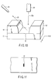
- sidewall
- pattern
- detector
- Prior art date
- Legal status (The legal status is an assumption and is not a legal conclusion. Google has not performed a legal analysis and makes no representation as to the accuracy of the status listed.)
- Granted
Links
Images

Classifications
-
- G—PHYSICS
- G03—PHOTOGRAPHY; CINEMATOGRAPHY; ANALOGOUS TECHNIQUES USING WAVES OTHER THAN OPTICAL WAVES; ELECTROGRAPHY; HOLOGRAPHY
- G03F—PHOTOMECHANICAL PRODUCTION OF TEXTURED OR PATTERNED SURFACES, e.g. FOR PRINTING, FOR PROCESSING OF SEMICONDUCTOR DEVICES; MATERIALS THEREFOR; ORIGINALS THEREFOR; APPARATUS SPECIALLY ADAPTED THEREFOR
- G03F1/00—Originals for photomechanical production of textured or patterned surfaces, e.g., masks, photo-masks, reticles; Mask blanks or pellicles therefor; Containers specially adapted therefor; Preparation thereof
- G03F1/68—Preparation processes not covered by groups G03F1/20 - G03F1/50
- G03F1/72—Repair or correction of mask defects
-
- H—ELECTRICITY
- H10—SEMICONDUCTOR DEVICES; ELECTRIC SOLID-STATE DEVICES NOT OTHERWISE PROVIDED FOR
- H10P—GENERIC PROCESSES OR APPARATUS FOR THE MANUFACTURE OR TREATMENT OF DEVICES COVERED BY CLASS H10
- H10P76/00—Manufacture or treatment of masks on semiconductor bodies, e.g. by lithography or photolithography
-
- G—PHYSICS
- G03—PHOTOGRAPHY; CINEMATOGRAPHY; ANALOGOUS TECHNIQUES USING WAVES OTHER THAN OPTICAL WAVES; ELECTROGRAPHY; HOLOGRAPHY
- G03F—PHOTOMECHANICAL PRODUCTION OF TEXTURED OR PATTERNED SURFACES, e.g. FOR PRINTING, FOR PROCESSING OF SEMICONDUCTOR DEVICES; MATERIALS THEREFOR; ORIGINALS THEREFOR; APPARATUS SPECIALLY ADAPTED THEREFOR
- G03F1/00—Originals for photomechanical production of textured or patterned surfaces, e.g., masks, photo-masks, reticles; Mask blanks or pellicles therefor; Containers specially adapted therefor; Preparation thereof
- G03F1/68—Preparation processes not covered by groups G03F1/20 - G03F1/50
- G03F1/72—Repair or correction of mask defects
- G03F1/74—Repair or correction of mask defects by charged particle beam [CPB], e.g. focused ion beam
-
- G—PHYSICS
- G03—PHOTOGRAPHY; CINEMATOGRAPHY; ANALOGOUS TECHNIQUES USING WAVES OTHER THAN OPTICAL WAVES; ELECTROGRAPHY; HOLOGRAPHY
- G03F—PHOTOMECHANICAL PRODUCTION OF TEXTURED OR PATTERNED SURFACES, e.g. FOR PRINTING, FOR PROCESSING OF SEMICONDUCTOR DEVICES; MATERIALS THEREFOR; ORIGINALS THEREFOR; APPARATUS SPECIALLY ADAPTED THEREFOR
- G03F1/00—Originals for photomechanical production of textured or patterned surfaces, e.g., masks, photo-masks, reticles; Mask blanks or pellicles therefor; Containers specially adapted therefor; Preparation thereof
- G03F1/26—Phase shift masks [PSM]; PSM blanks; Preparation thereof
Definitions
- the present invention relates generally to a method of correcting a photomask used for the manufacture of a semiconductor integrated circuit, and more particularly to a method of correcting a photomask by applying a focused ion beam (FIB) to a defect of the photomask to repair the defect.
- FIB focused ion beam
- one point drift correction is used in order to totally correct a drift of an image due to charge up, or a drift due to thermal expansion of a mask or a mask holder.
- a pinhole is formed in a pattern of the photomask. The beam is moved to the portion to be corrected by using the pinhole as a reference point, thereby enhancing correction accuracy.
- a specific example of the one point drift correction will be described below with reference to FIGS. 8 to 10.
- a focused ion beam 22a is applied to a part of a pattern 12 which is formed on a substrate 11 for a photomask, so that a pinhole 13, which serves as a reference point, is formed. Then, an ion beam 22b is applied from an ion beam source 21 to a scan region 14 including the pinhole 13. Secondary ions (secondary charged particles) 23 released from the portion where the pinhole 13 is formed are detected by a detector 24, thereby recognizing (obtaining) the reference point. Then, the positional relationship between the detected position of the pinhole 13 (position of the reference point) and the portion to be corrected which is known in advance, is calculated.
- the ion beam is applied to the portion to be corrected, thereby correcting the defect.
- the defect correction is completed. In this way, by confirming the reference point immediately before the defect correction processing, the influence of a drift can be reduced to a minimum.
- a round shape is ideal as the shape of a planar pattern of the reference point (pinhole) (refer, for example, to Jpn. Pat. Appln. KOKOKU Publication No. 5-4660).
- the pinhole is conventionally formed by applying the ion beam to a square-shaped area with an equal number of dots in longitudinal and horizontal directions (e.g. 4X4 dots).
- phase shift mask is used as a photomask
- a proper phase shift operation phase effect
- the pinhole is large relative to the pattern
- a region which affects a projected image is also large.
- the scan region for detecting the pinhole needs to be large.
- the beam scan damages a wide area of the pattern. Therefore, if the pattern is small, the line size of the projected image is small, which is a problem.
- the smaller the pattern the wider the region which affects the projected image.
- a detector 24 is disposed obliquely above the pinhole 13.
- the pattern of the pinhole has a square shape
- the following problem will arise. Since the detector 24 is disposed obliquely above the pinhole 13, the secondary ions 23 coming out of the pinhole 13 are considered to be blocked to some extent by a sidewall at the detector 24 side (the left sidewall in FIG. 10). Therefore, the length of the pinhole 13 in the X direction shown in FIG. 10 needs to be increased to a degree. In this case, if the pinhole 13 is a square pattern, the length of the pinhole 13 in the Y direction is equal to that in X direction.
- a secondary ion image 31 corresponding to the pinhole is a vertically elongated image in the Y direction.
- phase shift mask In the conventional method of correcting the photomask using one point drift correction, if the phase shift mask is used as a photomask, the region, where phase shift operation (phase effect) cannot be obtained, increases. Thus, a proper projected image cannot be obtained, which is a problem. There are also problems that the positional accuracy (recognition accuracy) of the reference pinhole is insufficient, and that the secondary ions (secondary charged particles) from the pinhole cannot efficiently be made incident on the detector.
- a method of correcting a photomask comprising: preparing a photomask substrate with a mask pattern including a phase shift pattern; forming a reference hole by removing a part of the mask pattern; applying an ion beam from an ion beam source to an area including the reference hole to allow secondary charged particles to be released from the reference hole; obtaining a position of the reference hole by detecting the secondary charged particles by a detector; calculating a positional relationship between the obtained position of the reference hole and a position of a defect of the mask pattern; and correcting the defect by applying an ion beam from the ion beam source to the defect, based on the calculated positional relationship, wherein a pattern of the reference hole, as viewed in a direction perpendicular to a top surface of the photomask substrate, is substantially rectangular, and a longitudinal direction of the rectangular pattern is parallel to a longitudinal direction of the phase shift pattern.
- a method of correcting a photomask comprising: preparing a photomask substrate having a mask pattern; forming a reference hole by removing a part of the mask pattern; applying an ion beam from an ion beam source to an area including the reference hole to allow secondary charged particles to be released from the reference hole; obtaining a position of the reference hole by detecting the secondary charged particles by a detector, a charged particle incidence portion of the detector being disposed obliquely above the reference hole; calculating a positional relationship between the obtained position of the reference hole and a position of a defect of the mask pattern; and correcting the defect by applying an ion beam from the ion beam source to the defect, based on the calculated positional relationship, wherein a pattern of the reference hole, as viewed in a direction perpendicular to a top surface of the photomask substrate, is substantially rectangular, and a longitudinal direction of the rectangular pattern is parallel to a straight line obtained by projecting, on
- a method of correcting a photomask comprising: preparing a photomask substrate having a mask pattern; forming a reference hole by removing a part of the mask pattern; applying an ion beam from an ion beam source to an area including the reference hole to allow secondary charged particles to be released from the reference hole; obtaining a position of the reference hole by detecting the secondary charged particles by a detector, a charged particle incidence portion of the detector being disposed obliquely above the reference hole; calculating a positional relationship between the obtained position of the reference hole and a position of a defect of the mask pattern; and correcting the defect by applying an ion beam from the ion beam source to the defect, based on the calculated positional relationship, wherein the reference hole is defined by a first sidewall located at the same side as the incidence portion of the detector, and a second sidewall opposed to the first sidewall, and an inclination of a plane linking a bottom end and an upper end of the
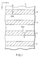
- FIG. 1 is a plan view showing one example of a photomask according to the embodiment of the present invention
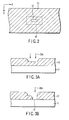
- FIG. 2 is a plan view showing the vicinity of a reference pinhole shown in FIG. 1
- FIGS. 3A and 3B are cross-sectional views (cross-sectional views in the X direction of FIG. 2) illustrating a method of forming the pinhole shown in FIG. 1
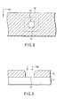
- FIG. 4 shows a method of detecting the pinhole shown in FIG. 1
- FIG. 5 shows a secondary ion image obtained by the method according to the embodiment of the present invention
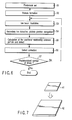
- FIG. 6 is a flow chart illustrating a method according to the embodiment of the present invention.
- phase shift mask such as a half tone phase shift mask or an embedded phase shift mask is prepared as a photomask, and is set in a correcting apparatus (step S1).
- the phase shift mask comprises a quartz substrate 11, and a phase shift pattern 12 (pattern for causing a phase effect) of a MoSi film, formed on the substrate 11.
- a focused ion beam is applied from an emission portion of an ion beam source onto the substrate 11 to form a pinhole 13, which serves as a reference point, in the pattern 12 (step S2).
- the planar pattern of the pinhole 13 is substantially rectangular, and the longitudinal direction (X direction) of the phase shift pattern 12 and that of the pattern of the pinhole 13 are substantially parallel.
- the ion beam is applied in a rectangular shape with 4 dots in the X direction and 1 dot in the Y direction.
- the pinhole 13 is formed in two separate stages, as shown in FIGS. 3A and 3B.
- the area to which the beam is applied is narrowed in the X direction, and a right-hand region of the pinhole 13 (in FIG. 3B) is selectively removed, thereby exposing the surface of the substrate 11.
- the sidewall of the pinhole 13 at the left side is recessed stepwise, from the bottom end of the sidewall towards the upper end.
- the inclination of the plane linking the bottom end and upper end of the left-hand sidewall in FIG.
- the sidewall is recessed in two stages, however, it may be recessed in three stages or more.
- the sidewall may also be recessed successively.
- the ion beam is applied to a scan region 14 (see FIG. 2) including the pinhole 13, and the position of the pinhole 13, which serves as a reference point, is detected (recognized or obtained) (steps S3, S4).
- an ion beam 22b is applied from the ion beam source 21 used for the pinhole formation, to the bottom surface of the pinhole 13, i.e., the exposed surface of the substrate 11.
- Secondary ions (secondary silicon ions) 23 released from the bottom surface of the pinhole 13 is detected by the detector 24 disposed obliquely above the pinhole 13.
- the distal end of the detector 24 is cylindrical.
- the substrate 11 having the phase shift pattern 12 formed is preset within the apparatus such that the parallel relationship as above can be obtained.
- a secondary ion image 31 obtained by the detector 24 is dot-shaped, as shown in FIG. 5.
- the positional relationship between the pinhole 13 and the correction portion 15 is calculated in a control apparatus (not shown) (step S5). For example, as shown in FIG. 1, if the position of the pinhole 13 is regarded as R(0,0), the position D(x,y) of the correction portion 15 can be determined.
- the position to which the ion beam from the ion beam source 21 is applied is returned to the position of the pinhole 13. After that, based on the positional relationship determined as described above, the position to which the ion beam is applied is moved to the position of the correction portion 15. Further, the ion beam is applied from the ion beam source 21 to the correction portion 15, thereby performing defect correction of the correction portion 15 (step S6). If the defect of the correction portion 15 is a pattern loss as shown in FIG. 1, correction is performed by depositing a carbon film while applying the ion beam to the loss portion. If the defect of the correction portion 15 is a pattern surplus, correction is performed by applying the ion beam to the surplus portion to perform etching.
- step S7 the required number of repeating steps S3 to S6 is performed (step S7). In this way, correction of the defect is completed.
- the repair process of the pinhole 13 is performed according to necessity.
- the photomask thus obtained is applied to the manufacture of a semiconductor device (integrated circuit device). Specifically, as shown in FIG. 7, the pattern of a photomask 41 is projected on a photoresist formed on a semiconductor substrate 42, thereby obtaining a fine pattern for forming an integrated circuit.
- the longitudinal direction of the rectangular pinhole pattern is parallel to the longitudinal direction of the phase shift pattern.
- the width of the short edge of the rectangular pattern is narrow.
- the width of the rectangular pattern narrows in the direction that light intensity distribution occurs due to the phase shift operation (phase effect). It is therefore possible to reduce the area that reduces the phase effect. Even if the size (line width) of the phase shift pattern is small, there is no need to correct a pinhole mark. If the pinhole mark is corrected, the area whose phase effect is degraded by the carbon film deposited for correction can be reduced to a minimum. Since the width of the pinhole is narrow, the scan region at the time of detecting the pinhole is also narrow. Thus, damage of the beam scan to the pattern can be suppressed to a minimum. As described above, in the embodiment of the present invention, the influence of the reference pinhole can be suppressed to a minimum, and one point drift correction can be performed effectively.
- the planar pattern of the pinhole is relatively long in the X direction, and relatively short in the Y direction.
- a sufficient amount of secondary ions can arrive at the detector.
- the pinhole position detection accuracy can be improved. That is, in the X direction, a certain extent of position detection accuracy and secondary ion arrival amount can be obtained, as in the prior art.
- Concerning the Y direction the position detection accuracy can be considerably improved compared with the prior art, by narrowing the width of the pinhole.
- the sidewall at the detector side is inclined successively or in stages.
- the average inclination thereof is gentle.
- the ratio of the secondary charged particles which are blocked by the sidewall at the detector side can be reduced.
- the sidewall of the pinhole 13 at the detector 24 side is inclined.
- the inclination angle of the plane linking the upper end and bottom end of the sidewall is made equal to the inclination angle of the straight line linking the distal end of the detector 24 and the pinhole 13.
- the secondary ions can arrive at the detector with efficiency. Even if the bottom surface of the pinhole 13 is small, the yield reduction of the secondary ion can be suppressed, and damage to the substrate can be reduced.
- an ordinary mask a so-called binary mask, typically, a chrome mask
Landscapes
- Physics & Mathematics (AREA)
- General Physics & Mathematics (AREA)
- Preparing Plates And Mask In Photomechanical Process (AREA)
Abstract
Description
Claims (16)
- A method of correcting a photomask, characterized by comprising:wherein a pattern of the reference hole, as viewed in a direction perpendicular to a top surface of the photomask substrate, is substantially rectangular, and a longitudinal direction of the rectangular pattern is parallel to a longitudinal direction of the phase shift pattern.preparing a photomask substrate (11) with a mask pattern (12) including a phase shift pattern;forming a reference hole (13) by removing a part of the mask pattern;applying an ion beam (22b) from an ion beam source (21) to an area including the reference hole to allow secondary charged particles (23) to be released from the reference hole;obtaining a position of the reference hole by detecting the secondary charged particles by a detector (24);calculating a positional relationship between the obtained position of the reference hole and a position of a defect (15) of the mask pattern; andcorrecting the defect by applying an ion beam from the ion beam source to the defect, based on the calculated positional relationship,
- A method according to claim 1, characterized in that a charged particle incidence portion of the detector is disposed obliquely above the reference hole, and the longitudinal direction of the rectangular pattern is parallel to a straight line obtained by projecting, on the top surface of the photomask substrate, a straight line linking the incidence portion of the detector and the reference hole.
- A method according to claim 2, characterized in that the reference hole is defined by a first sidewall located at the same side as the incidence portion of the detector, and a second sidewall opposed to the first sidewall, and an inclination of a plane linking a bottom end and an upper end of the first sidewall is more gentle than that of a plane linking a bottom end and an upper end of the second sidewall.
- A method according to claim 1, characterized in that a charged particle incidence portion of the detector is disposed obliquely above the reference hole, the reference hole is defined by a first sidewall located at the same side as the incidence portion of the detector, and a second sidewall opposed to the first sidewall, and an inclination of a plane linking a bottom end and an upper end of the first sidewall is more gentle than that of a plane linking a bottom end and an upper end of the second sidewall.
- A method according to claim 1, characterized in that the reference hole is formed by applying an ion beam from the ion beam source.
- A method according to claim 1, characterized in that a series of processes from applying the ion beam to the area including the reference hole to correcting the defect is performed a plurality of times.
- A method of correcting a photomask, characterized by comprising:wherein a pattern of the reference hole, as viewed in a direction perpendicular to a top surface of the photomask substrate, is substantially rectangular, and a longitudinal direction of the rectangular pattern is parallel to a straight line obtained by projecting, on the top surface of the photomask substrate, a straight line linking the incidence portion of the detector and the reference hole.preparing a photomask substrate (11) having a mask pattern (12);forming a reference hole (13) by removing a part of the mask pattern;applying an ion beam (22b) from an ion beam source (21) to an area including the reference hole to allow secondary charged particles (23) to be released from the reference hole;obtaining a position of the reference hole by detecting the secondary charged particles by a detector (24), a charged particle incidence portion of the detector being disposed obliquely above the reference hole;calculating a positional relationship between the obtained position of the reference hole and a position of a defect (15) of the mask pattern; andcorrecting the defect by applying an ion beam from the ion beam source to the defect, based on the calculated positional relationship,
- A method according to claim 7, characterized in that the reference hole is defined by a first sidewall located at the same side as the incidence portion of the detector, and a second sidewall opposed to the first sidewall, and an inclination of a plane linking a bottom end and an upper end of the first sidewall is more gentle than that of a plane linking a bottom end and an upper end of the second sidewall.
- A method according to claim 7, characterized in that the reference hole is formed by applying an ion beam from the ion beam source.
- A method according to claim 7, characterized in that a series of processes from applying the ion beam to the area including the reference hole to correcting the defect is performed a plurality of times.
- A method of correcting a photomask, characterized by comprising:wherein the reference hole is defined by a first sidewall located at the same side as the incidence portion of the detector, and a second sidewall opposed to the first sidewall, and an inclination of a plane linking a bottom end and an upper end of the first sidewall is more gentle than that of a plane linking a bottom end and an upper end of the second side wall.preparing a photomask substrate (11) having a mask pattern (12);forming a reference hole (13) by removing a part of the mask pattern;applying an ion beam (22b) from an ion beam source (21) to an area including the reference hole to allow secondary charged particles (23) to be released from the reference hole;obtaining a position of the reference hole by detecting the secondary charged particles by a detector (24), a charged particle incidence portion of the detector being disposed obliquely above the reference hole;calculating a positional relationship between the obtained position of the reference hole and a position of a defect (15) of the mask pattern; andcorrecting the defect by applying an ion beam from the ion beam source to the defect, based on the calculated positional relationship,
- A method according to claim 11, characterized in that the reference hole is formed by applying an ion beam from the ion beam source.
- A method according to claim 11, characterized in that a series of processes from applying the ion beam to the area including the reference hole to correcting the defect is performed a plurality of times.
- A method of manufacturing a semiconductor device characterized by comprising projecting a pattern on a semiconductor substrate (42) using the photomask (41) corrected by the method according to claim 1.
- A method of manufacturing a semiconductor device characterized by comprising projecting a pattern on a semiconductor substrate (42) using the photomask (41) corrected by the method according to claim 7.
- A method of manufacturing a semiconductor device characterized by comprising projecting a pattern on a semiconductor substrate (42) using the photomask (41) corrected by the method according to claim 11.
Applications Claiming Priority (2)
| Application Number | Priority Date | Filing Date | Title |
|---|---|---|---|
| JP2001028553A JP4149676B2 (en) | 2001-02-05 | 2001-02-05 | Photomask correction method |
| JP2001028553 | 2001-02-05 |
Publications (3)
| Publication Number | Publication Date |
|---|---|
| EP1229385A2 true EP1229385A2 (en) | 2002-08-07 |
| EP1229385A3 EP1229385A3 (en) | 2003-12-10 |
| EP1229385B1 EP1229385B1 (en) | 2004-09-29 |
Family
ID=18893032
Family Applications (1)
| Application Number | Title | Priority Date | Filing Date |
|---|---|---|---|
| EP02001992A Expired - Lifetime EP1229385B1 (en) | 2001-02-05 | 2002-02-05 | Method of correcting a photomask and method of manufacturing a semiconductor device |
Country Status (7)
| Country | Link |
|---|---|
| US (1) | US6740456B2 (en) |
| EP (1) | EP1229385B1 (en) |
| JP (1) | JP4149676B2 (en) |
| KR (1) | KR100455536B1 (en) |
| CN (1) | CN1207631C (en) |
| DE (1) | DE60201358T2 (en) |
| TW (1) | TWI223125B (en) |
Cited By (1)
| Publication number | Priority date | Publication date | Assignee | Title |
|---|---|---|---|---|
| CN1530743B (en) * | 2003-03-12 | 2013-03-06 | 住友化学株式会社 | Light mask and diffuse-reflecting board |
Families Citing this family (18)
| Publication number | Priority date | Publication date | Assignee | Title |
|---|---|---|---|---|
| JP4137329B2 (en) * | 2000-01-11 | 2008-08-20 | エスアイアイ・ナノテクノロジー株式会社 | Focused ion beam processing method |
| CN1726431A (en) * | 2002-10-21 | 2006-01-25 | 纳米墨水公司 | Nanometer-scale engineered structures, methods and apparatus for fabrication thereof, and applications to mask repair, enhancement, and fabrications |
| JP4286555B2 (en) * | 2003-02-18 | 2009-07-01 | エスアイアイ・ナノテクノロジー株式会社 | Ion beam processing method |
| US7289123B2 (en) * | 2004-09-30 | 2007-10-30 | Microsoft Corporation | Simplifying complex characters to maintain legibility |
| US8124300B1 (en) * | 2004-11-30 | 2012-02-28 | Globalfoundries Inc. | Method of lithographic mask correction using localized transmission adjustment |
| JP4559921B2 (en) * | 2005-06-20 | 2010-10-13 | エスアイアイ・ナノテクノロジー株式会社 | Gray tone pattern film defect correction method |
| KR100924342B1 (en) * | 2007-10-15 | 2009-10-30 | 주식회사 하이닉스반도체 | How to fix defects in the photomask |
| CN101430500B (en) * | 2007-11-06 | 2011-05-11 | 中芯国际集成电路制造(上海)有限公司 | OPC correcting method for forming auxiliary through hole |
| US9721754B2 (en) * | 2011-04-26 | 2017-08-01 | Carl Zeiss Smt Gmbh | Method and apparatus for processing a substrate with a focused particle beam |
| US9139661B2 (en) * | 2012-06-25 | 2015-09-22 | Yagna Limited | Methods for biocompatible derivitization of cellulosic surfaces |
| CN105981326B (en) | 2014-02-26 | 2019-05-14 | 三菱电机株式会社 | Certificate management apparatus and certificate management method |
| DE102018209562B3 (en) | 2018-06-14 | 2019-12-12 | Carl Zeiss Smt Gmbh | Apparatus and methods for inspecting and / or processing an element for photolithography |
| DE102018217025A1 (en) | 2018-10-04 | 2019-10-17 | Carl Zeiss Smt Gmbh | Method and apparatus for analyzing a substrate |
| CN109659246B (en) * | 2018-11-15 | 2020-12-01 | 长江存储科技有限责任公司 | A method for measuring the inclination of an opening and a method for preparing a three-dimensional memory |
| DE102019200696B4 (en) | 2019-01-21 | 2022-02-10 | Carl Zeiss Smt Gmbh | Apparatus, method and computer program for determining a position of an element on a photolithographic mask |
| DE102021210019A1 (en) | 2021-09-10 | 2023-03-16 | Carl Zeiss Smt Gmbh | Method and apparatus for repairing a defect in a sample using a focused particle beam |
| DE102021213163A1 (en) | 2021-11-23 | 2023-05-25 | Carl Zeiss Smt Gmbh | Method and device for calibrating an operation on a photomask |
| CN115047710B (en) * | 2022-06-30 | 2026-02-13 | 上海集成电路装备材料产业创新中心有限公司 | Methods for locating and eliminating defects in photomasks |
Family Cites Families (10)
| Publication number | Priority date | Publication date | Assignee | Title |
|---|---|---|---|---|
| JPS5832147A (en) * | 1981-08-20 | 1983-02-25 | Fujitsu Ltd | Inspecting method for reticle |
| JP2543680B2 (en) | 1985-10-02 | 1996-10-16 | セイコー電子工業株式会社 | Mask repair device |
| JPS63305358A (en) | 1987-06-05 | 1988-12-13 | Seiko Instr & Electronics Ltd | Method for working pattern film |
| US5260771A (en) * | 1988-03-07 | 1993-11-09 | Hitachi, Ltd. | Method of making semiconductor integrated circuit, pattern detecting method, and system for semiconductor alignment and reduced stepping exposure for use in same |
| KR950000091B1 (en) * | 1990-06-20 | 1995-01-09 | 후지쓰 가부시끼가이샤 | Reticle having phase shifter and manufacturing method thereof and correcting method |
| JPH054660A (en) | 1991-06-18 | 1993-01-14 | Seiko Epson Corp | Packing cushioning material and manufacturing method thereof |
| JPH0883753A (en) * | 1994-09-13 | 1996-03-26 | Nikon Corp | Focal point detecting method |
| US5696587A (en) | 1994-12-14 | 1997-12-09 | United Microelectronics Corporation | Metal target for laser repair of dies |
| JPH10261563A (en) * | 1997-03-18 | 1998-09-29 | Nikon Corp | Projection exposure method and apparatus |
| JP3274396B2 (en) * | 1997-11-07 | 2002-04-15 | 株式会社東芝 | Pattern measurement method |
-
2001
- 2001-02-05 JP JP2001028553A patent/JP4149676B2/en not_active Expired - Fee Related
-
2002
- 2002-02-04 KR KR10-2002-0006184A patent/KR100455536B1/en not_active Expired - Fee Related
- 2002-02-04 US US10/061,327 patent/US6740456B2/en not_active Expired - Lifetime
- 2002-02-05 TW TW091101992A patent/TWI223125B/en not_active IP Right Cessation
- 2002-02-05 CN CNB021035377A patent/CN1207631C/en not_active Expired - Fee Related
- 2002-02-05 DE DE60201358T patent/DE60201358T2/en not_active Expired - Fee Related
- 2002-02-05 EP EP02001992A patent/EP1229385B1/en not_active Expired - Lifetime
Cited By (1)
| Publication number | Priority date | Publication date | Assignee | Title |
|---|---|---|---|---|
| CN1530743B (en) * | 2003-03-12 | 2013-03-06 | 住友化学株式会社 | Light mask and diffuse-reflecting board |
Also Published As
| Publication number | Publication date |
|---|---|
| JP2002229185A (en) | 2002-08-14 |
| KR100455536B1 (en) | 2004-11-06 |
| JP4149676B2 (en) | 2008-09-10 |
| KR20020065366A (en) | 2002-08-13 |
| CN1369745A (en) | 2002-09-18 |
| EP1229385B1 (en) | 2004-09-29 |
| TWI223125B (en) | 2004-11-01 |
| DE60201358D1 (en) | 2004-11-04 |
| US20020122992A1 (en) | 2002-09-05 |
| CN1207631C (en) | 2005-06-22 |
| DE60201358T2 (en) | 2005-10-13 |
| EP1229385A3 (en) | 2003-12-10 |
| US6740456B2 (en) | 2004-05-25 |
Similar Documents
| Publication | Publication Date | Title |
|---|---|---|
| EP1229385B1 (en) | Method of correcting a photomask and method of manufacturing a semiconductor device | |
| US5799104A (en) | Mask defect repair system and method | |
| US6991878B2 (en) | Photomask repair method and apparatus | |
| JP5116996B2 (en) | Charged particle beam drawing method, exposure apparatus, and device manufacturing method | |
| JP6858732B2 (en) | OPC method and mask manufacturing method using the OPC method | |
| JP6750966B2 (en) | Pattern inspection device and pattern inspection method | |
| JPH07122484A (en) | Pattern correction method in pattern correction device of electron beam drawing apparatus | |
| US6933081B2 (en) | Method for quartz bump defect repair with less substrate damage | |
| US6182369B1 (en) | Pattern forming apparatus | |
| JP2023513667A (en) | Multi-step process inspection method | |
| JP2001085300A (en) | Mark detection method, electron beam device, and semiconductor device manufacturing method | |
| JP4112842B2 (en) | Mask defect correction method | |
| JP2000010260A (en) | Black defect repair method for mask repair device | |
| US6605398B2 (en) | Methods and apparatus for controlling beam blur in charged-particle-beam microlithography | |
| JP2004287321A (en) | Photomask defect repair method | |
| US6541779B2 (en) | Charged-particle-beam microlithography apparatus including selectable systems for determining alignment-mark position, and device-fabrication methods utilizing same | |
| US6821688B2 (en) | Photomask, method for manufacturing the same and method for detecting/repairing defects in photomask | |
| JP3258213B2 (en) | How to fix the pattern film | |
| JP2008004596A (en) | Charged particle beam drawing method, exposure apparatus, and device manufacturing method | |
| JP2888228B2 (en) | Structure of partial mask for charged particle beam | |
| JP3849498B2 (en) | Stencil mask defect correcting apparatus and stencil mask defect correcting method | |
| JPH04289861A (en) | How to modify a mask | |
| JP2002072456A (en) | Reticle repair method, reticle obtained thereby and reticle repair device | |
| JPH04297016A (en) | How to make an X-ray mask | |
| JP2002075828A (en) | Proximity effect correction method, electron beam projection exposure apparatus, and device manufacturing method |
Legal Events
| Date | Code | Title | Description |
|---|---|---|---|
| PUAI | Public reference made under article 153(3) epc to a published international application that has entered the european phase |
Free format text: ORIGINAL CODE: 0009012 |
|
| 17P | Request for examination filed |
Effective date: 20020205 |
|
| AK | Designated contracting states |
Kind code of ref document: A2 Designated state(s): AT BE CH CY DE DK ES FI FR GB GR IE IT LI LU MC NL PT SE TR |
|
| AX | Request for extension of the european patent |
Free format text: AL;LT;LV;MK;RO;SI |
|
| PUAL | Search report despatched |
Free format text: ORIGINAL CODE: 0009013 |
|
| AK | Designated contracting states |
Kind code of ref document: A3 Designated state(s): AT BE CH CY DE DK ES FI FR GB GR IE IT LI LU MC NL PT SE TR |
|
| AX | Request for extension of the european patent |
Extension state: AL LT LV MK RO SI |
|
| GRAP | Despatch of communication of intention to grant a patent |
Free format text: ORIGINAL CODE: EPIDOSNIGR1 |
|
| GRAS | Grant fee paid |
Free format text: ORIGINAL CODE: EPIDOSNIGR3 |
|
| GRAA | (expected) grant |
Free format text: ORIGINAL CODE: 0009210 |
|
| AKX | Designation fees paid |
Designated state(s): BE DE FR IT NL |
|
| AK | Designated contracting states |
Kind code of ref document: B1 Designated state(s): BE DE FR IT NL |
|
| REG | Reference to a national code |
Ref country code: IE Ref legal event code: FG4D |
|
| REF | Corresponds to: |
Ref document number: 60201358 Country of ref document: DE Date of ref document: 20041104 Kind code of ref document: P |
|
| PLBE | No opposition filed within time limit |
Free format text: ORIGINAL CODE: 0009261 |
|
| STAA | Information on the status of an ep patent application or granted ep patent |
Free format text: STATUS: NO OPPOSITION FILED WITHIN TIME LIMIT |
|
| ET | Fr: translation filed | ||
| 26N | No opposition filed |
Effective date: 20050630 |
|
| PGFP | Annual fee paid to national office [announced via postgrant information from national office to epo] |
Ref country code: DE Payment date: 20080221 Year of fee payment: 7 Ref country code: IT Payment date: 20080212 Year of fee payment: 7 Ref country code: NL Payment date: 20080229 Year of fee payment: 7 |
|
| PGFP | Annual fee paid to national office [announced via postgrant information from national office to epo] |
Ref country code: FR Payment date: 20080111 Year of fee payment: 7 |
|
| PGFP | Annual fee paid to national office [announced via postgrant information from national office to epo] |
Ref country code: BE Payment date: 20080205 Year of fee payment: 7 |
|
| BERE | Be: lapsed |
Owner name: *DAI NIPPON PRINTING CO. LTD Effective date: 20090228 Owner name: *TOSHIBA K.K. Effective date: 20090228 |
|
| NLV4 | Nl: lapsed or anulled due to non-payment of the annual fee |
Effective date: 20090901 |
|
| REG | Reference to a national code |
Ref country code: FR Ref legal event code: ST Effective date: 20091030 |
|
| PG25 | Lapsed in a contracting state [announced via postgrant information from national office to epo] |
Ref country code: NL Free format text: LAPSE BECAUSE OF NON-PAYMENT OF DUE FEES Effective date: 20090901 |
|
| PG25 | Lapsed in a contracting state [announced via postgrant information from national office to epo] |
Ref country code: DE Free format text: LAPSE BECAUSE OF NON-PAYMENT OF DUE FEES Effective date: 20090901 |
|
| PG25 | Lapsed in a contracting state [announced via postgrant information from national office to epo] |
Ref country code: BE Free format text: LAPSE BECAUSE OF NON-PAYMENT OF DUE FEES Effective date: 20090228 |
|
| PG25 | Lapsed in a contracting state [announced via postgrant information from national office to epo] |
Ref country code: FR Free format text: LAPSE BECAUSE OF NON-PAYMENT OF DUE FEES Effective date: 20090302 |
|
| PG25 | Lapsed in a contracting state [announced via postgrant information from national office to epo] |
Ref country code: IT Free format text: LAPSE BECAUSE OF NON-PAYMENT OF DUE FEES Effective date: 20090205 |