EP1228394B1 - Gepolte wellenleiterstruktur mit stabilisiertem internen elektrischen feld - Google Patents
Gepolte wellenleiterstruktur mit stabilisiertem internen elektrischen feld Download PDFInfo
- Publication number
- EP1228394B1 EP1228394B1 EP00972435A EP00972435A EP1228394B1 EP 1228394 B1 EP1228394 B1 EP 1228394B1 EP 00972435 A EP00972435 A EP 00972435A EP 00972435 A EP00972435 A EP 00972435A EP 1228394 B1 EP1228394 B1 EP 1228394B1
- Authority
- EP
- European Patent Office
- Prior art keywords
- region
- electric field
- waveguide structure
- optical waveguide
- electrode
- Prior art date
- Legal status (The legal status is an assumption and is not a legal conclusion. Google has not performed a legal analysis and makes no representation as to the accuracy of the status listed.)
- Expired - Lifetime
Links
Images

Classifications
-
- C—CHEMISTRY; METALLURGY
- C03—GLASS; MINERAL OR SLAG WOOL
- C03B—MANUFACTURE, SHAPING, OR SUPPLEMENTARY PROCESSES
- C03B37/00—Manufacture or treatment of flakes, fibres, or filaments from softened glass, minerals, or slags
- C03B37/01—Manufacture of glass fibres or filaments
- C03B37/012—Manufacture of preforms for drawing fibres or filaments
- C03B37/01205—Manufacture of preforms for drawing fibres or filaments starting from tubes, rods, fibres or filaments
- C03B37/01225—Means for changing or stabilising the shape, e.g. diameter, of tubes or rods in general, e.g. collapsing
- C03B37/01228—Removal of preform material
- C03B37/01231—Removal of preform material to form a longitudinal hole, e.g. by drilling
-
- C—CHEMISTRY; METALLURGY
- C03—GLASS; MINERAL OR SLAG WOOL
- C03B—MANUFACTURE, SHAPING, OR SUPPLEMENTARY PROCESSES
- C03B37/00—Manufacture or treatment of flakes, fibres, or filaments from softened glass, minerals, or slags
- C03B37/01—Manufacture of glass fibres or filaments
- C03B37/012—Manufacture of preforms for drawing fibres or filaments
- C03B37/014—Manufacture of preforms for drawing fibres or filaments made entirely or partially by chemical means, e.g. vapour phase deposition of bulk porous glass either by outside vapour deposition [OVD], or by outside vapour phase oxidation [OVPO] or by vapour axial deposition [VAD]
- C03B37/018—Manufacture of preforms for drawing fibres or filaments made entirely or partially by chemical means, e.g. vapour phase deposition of bulk porous glass either by outside vapour deposition [OVD], or by outside vapour phase oxidation [OVPO] or by vapour axial deposition [VAD] by glass deposition on a glass substrate, e.g. by inside-, modified-, plasma- or plasma modified- chemical vapour deposition [ICVD, MCVD, PCVD, PMCVD], i.e. by thin layer coating on the inside or outside of a glass tube or on a glass rod
- C03B37/01884—Means for supporting, rotating and translating tubes or rods being formed, e.g. lathes
- C03B37/01892—Deposition substrates, e.g. tubes, mandrels
-
- G—PHYSICS
- G02—OPTICS
- G02F—OPTICAL DEVICES OR ARRANGEMENTS FOR THE CONTROL OF LIGHT BY MODIFICATION OF THE OPTICAL PROPERTIES OF THE MEDIA OF THE ELEMENTS INVOLVED THEREIN; NON-LINEAR OPTICS; FREQUENCY-CHANGING OF LIGHT; OPTICAL LOGIC ELEMENTS; OPTICAL ANALOGUE/DIGITAL CONVERTERS
- G02F1/00—Devices or arrangements for the control of the intensity, colour, phase, polarisation or direction of light arriving from an independent light source, e.g. switching, gating or modulating; Non-linear optics
- G02F1/01—Devices or arrangements for the control of the intensity, colour, phase, polarisation or direction of light arriving from an independent light source, e.g. switching, gating or modulating; Non-linear optics for the control of the intensity, phase, polarisation or colour
- G02F1/011—Devices or arrangements for the control of the intensity, colour, phase, polarisation or direction of light arriving from an independent light source, e.g. switching, gating or modulating; Non-linear optics for the control of the intensity, phase, polarisation or colour in optical waveguides, not otherwise provided for in this subclass
- G02F1/0115—Devices or arrangements for the control of the intensity, colour, phase, polarisation or direction of light arriving from an independent light source, e.g. switching, gating or modulating; Non-linear optics for the control of the intensity, phase, polarisation or colour in optical waveguides, not otherwise provided for in this subclass in optical fibres
-
- G—PHYSICS
- G02—OPTICS
- G02F—OPTICAL DEVICES OR ARRANGEMENTS FOR THE CONTROL OF LIGHT BY MODIFICATION OF THE OPTICAL PROPERTIES OF THE MEDIA OF THE ELEMENTS INVOLVED THEREIN; NON-LINEAR OPTICS; FREQUENCY-CHANGING OF LIGHT; OPTICAL LOGIC ELEMENTS; OPTICAL ANALOGUE/DIGITAL CONVERTERS
- G02F1/00—Devices or arrangements for the control of the intensity, colour, phase, polarisation or direction of light arriving from an independent light source, e.g. switching, gating or modulating; Non-linear optics
- G02F1/35—Non-linear optics
- G02F1/37—Non-linear optics for second-harmonic generation
- G02F1/377—Non-linear optics for second-harmonic generation in an optical waveguide structure
- G02F1/383—Non-linear optics for second-harmonic generation in an optical waveguide structure of the optical fibre type
-
- G—PHYSICS
- G02—OPTICS
- G02F—OPTICAL DEVICES OR ARRANGEMENTS FOR THE CONTROL OF LIGHT BY MODIFICATION OF THE OPTICAL PROPERTIES OF THE MEDIA OF THE ELEMENTS INVOLVED THEREIN; NON-LINEAR OPTICS; FREQUENCY-CHANGING OF LIGHT; OPTICAL LOGIC ELEMENTS; OPTICAL ANALOGUE/DIGITAL CONVERTERS
- G02F1/00—Devices or arrangements for the control of the intensity, colour, phase, polarisation or direction of light arriving from an independent light source, e.g. switching, gating or modulating; Non-linear optics
- G02F1/35—Non-linear optics
- G02F1/355—Non-linear optics characterised by the materials used
- G02F1/3558—Poled materials, e.g. with periodic poling; Fabrication of domain inverted structures, e.g. for quasi-phase-matching [QPM]
-
- G—PHYSICS
- G02—OPTICS
- G02F—OPTICAL DEVICES OR ARRANGEMENTS FOR THE CONTROL OF LIGHT BY MODIFICATION OF THE OPTICAL PROPERTIES OF THE MEDIA OF THE ELEMENTS INVOLVED THEREIN; NON-LINEAR OPTICS; FREQUENCY-CHANGING OF LIGHT; OPTICAL LOGIC ELEMENTS; OPTICAL ANALOGUE/DIGITAL CONVERTERS
- G02F2201/00—Constructional arrangements not provided for in groups G02F1/00 - G02F7/00
- G02F2201/02—Constructional arrangements not provided for in groups G02F1/00 - G02F7/00 fibre
-
- G—PHYSICS
- G02—OPTICS
- G02F—OPTICAL DEVICES OR ARRANGEMENTS FOR THE CONTROL OF LIGHT BY MODIFICATION OF THE OPTICAL PROPERTIES OF THE MEDIA OF THE ELEMENTS INVOLVED THEREIN; NON-LINEAR OPTICS; FREQUENCY-CHANGING OF LIGHT; OPTICAL LOGIC ELEMENTS; OPTICAL ANALOGUE/DIGITAL CONVERTERS
- G02F2202/00—Materials and properties
- G02F2202/07—Materials and properties poled
Definitions
- the present invention relates broadly to optical waveguides, and in particular, waveguides suitable for being poled.
- Inducing a polarisation in a material involves exposing the material to an intense electric filed, usually whilst the material is either subjected to a heating process or a UV irradiation.
- the poling process may effect a change in the optical second-order non-linearity.
- twin-hole fibre structure When the material comprises the core of an optical fibre, a twin-hole fibre structure is typically used for poling.
- a twin-hole fibre two longitudinal holes are located in the silica cladding on opposite sides of the core, and each hole contains a wire-like electrode. A poling voltage applied across the electrodes generates the electric field for poling the core.
- a positively-charged layer forms in the material around at least one of the electrodes and a negatively-charged layer forms adjacent and around the positively-charged layer.
- the positively-charged layer forms near and around the periphery of at least one of the longitudinal holes and the negatively-charged layer forms separately from and around the outer circumference of positively-charged layer.
- WO 90/08970 discloses the application of intense external electric fields across a fibre core, for imparting to the fibre a permanent linear electro-optic property.
- the external electric field is sustained for a prolonged period of time, and poling may be accelerated by performing this method at an elevated temperature.
- This document also teaches the use of one or two internal electrodes incorporated in the fibre cladding, and the fabrication of such internal electrodes from a metal or metal alloy that is a liquid at poling temperature.
- the invention provides an optical waveguide structure as claimed in claim 1 or claim 10.
- the internal electric field is a result of a space charge induced in the region by the external electric field, and the region acts to inhibit decay of the space charge.
- the region acts to inhibit decay of an optical second-order non-linearity induced in the region as a result of poling with the external electric field.
- the region may comprise a charge-trapping material, a charge-donating material, or both a charge-trapping material and a charge-donating material.
- the structure may be in the form of an optical fibre.
- the structure may be the form of a planar optical waveguide.
- the optical fibre includes a hole extending longitudinally in the optical fibre, wherein the hole is arranged to receive an electrode, and the region is arranged circumferentially around the hole.
- the waveguide structure may comprise a tunable coupler, a phase modulator, a tunable attenuator, a tunable broad band filter, a tunable narrow band filter, a tunable Bragg grating device, a router, a switch, an intensity modulator, a travelling wave modulator, a non-linear optical device such as a SHG, THG, electrically tunable laser, or a sensor such as a voltage sensor.
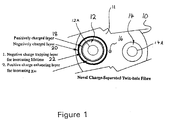
- a twin-hole fibre 10 comprises cladding 11 in which two longitudinal holes 12, 14 extend along the fibre 10.
- a core 16 of the optical fibre 10 is located between the holes 12, 14.
- Each hole 12, 14 contains an electrode 12A, 14A extending longitudinally in the hole.
- the poling voltage induces a positively-charged layer 18 around one of the holes 12, and a negatively-charged layer 20 around the positively-charged layer.
- the charged layers 18, 20 occur around the hole containing the anode.
- a region 22 extends circumferentially around the hole 12 and between the positively-charged layer 18 and the negatively-charged layer 20.
- the region 22 may comprise a charge-trapping material or a charge-donating material.
- the optical fibre 10 is silica-based, and the region 22 comprises a borosilicate glass. It is believed that the borosilicate maintains an internal electric field in the region 22 after the external electric field has been removed, by inhibiting charge-neutralisation between the charged layers 18, 20. It is thought the borosilicate achieves this by trapping electrons at the boron sites of the borosilicate.
- the borosilicate maintains a space charge which forms during poling, thus giving rise to a persistent or "frozen-in” electric field which remains after the poling voltage is removed. It is further believed that the frozen-in electric field stabilises an optical second-order non-linearity which is induced in the silica while the poling voltage is applied.
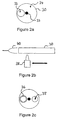
- a pre-form 30 for the optical fibre shown in Figure 1 is produced by firstly drilling one hole 32 into the pre-form 30.
- the hole 32 is located in the cladding 31 around the core 33 of the pre-form 30.
- a borosilicate region 36 is then formed using a chemical vapour deposition technique to deposit a layer of borosilicate.
- the technique involves periodically scanning a heating flame 38 along a length of the pre-form 30, whilst a vapour 40 including borosilicate is directed towards the end face of the pre-form 30. A portion of the vapour 40 enters the hole 32 and impinges on the internal surface of the hole 32. The preform is rotated whilst the flame 38 is periodically scanned.
- the decay of space charge induced in the borosilicate layer during poling is inhibited, which in turn inhibits the decay of the induced second-order non-linearity X (2) .
- the second-order non-linearity initially decays by about 20 %, instead of about 60 % for the standard twin-hole fibre (curve 52).
- the decay rate after about 17 hours is flatter for the fibre embodying the present invention (curve 50).
Landscapes
- Physics & Mathematics (AREA)
- Chemical & Material Sciences (AREA)
- Nonlinear Science (AREA)
- Engineering & Computer Science (AREA)
- Geochemistry & Mineralogy (AREA)
- Manufacturing & Machinery (AREA)
- Materials Engineering (AREA)
- Organic Chemistry (AREA)
- Life Sciences & Earth Sciences (AREA)
- General Life Sciences & Earth Sciences (AREA)
- General Physics & Mathematics (AREA)
- Optics & Photonics (AREA)
- Chemical Kinetics & Catalysis (AREA)
- General Chemical & Material Sciences (AREA)
- Optical Integrated Circuits (AREA)
Claims (10)
- Eine Lichtwellenleiterstruktur (10), die angeordnet ist, um elektrisch gepolt zu sein, die eine Elektrode (12A, 14A) oder einen Abschnitt (12, 14) umfasst, der angepasst ist, um eine Elektrode (12A, 14A) aufzunehmen, dadurch gekennzeichnet, dass:die Wellenleiterstruktur (10) eine Region (22, 36) umfasst, die ein Ladungseinfangmaterial nahe oder benachbart zu der Elektrode (12A, 14A) oder dem Abschnitt (12, 14) umfasst, wobei die Region (22, 36), wenn dieselbe mit einem äußeren elektrischen Feld gepolt ist, wirkt, um ein inneres elektrisches Feld in der Region (22, 36) und zwischen einer positiv geladenen Region (18) und einer negativ geladenen Region (20), die durch das Polieren induziert wird, zu stabilisieren, nachdem das äußere elektrische Feld entfernt wurde.
- Die Lichtwellenleiterstruktur gemäß Anspruch 1, bei der das innere elektrische Feld ein Ergebnis einer Raumladung ist, die durch das äußere elektrische Feld in die Region (22, 36) induziert wird, und die Region wirkt, um das Abfallen der Raumladung zu blockieren.
- Die Lichtwellenleiterstruktur (10) gemäß Anspruch 1 oder Anspruch 2, bei der die Region (22, 36) wirkt, um das Abfallen einer optischen Nichtlinearität zweiter Ordnung zu blockieren, die als eine Folge des Polierens mit dem äußeren elektrischen Feld in die Region (22, 36) induziert wird.
- Die Lichtwellenleiterstruktur (10) gemäß einem der vorhergehenden Ansprüche, bei der der Wellenleiter aus einem Siliziumdioxid-basierten Material gebildet ist.
- Die Lichtwellenleiterstruktur (10) gemäß einem der vorhergehenden Ansprüche, bei der die Region (22, 36) Borsilikat umfasst.
- Die Lichtwellenleiterstruktur (10) gemäß einem der vorhergehenden Ansprüche, wobei die Struktur (10) einen planaren optischen Wellenleiter umfasst.
- Die Lichtwellenleiterstruktur (10) gemäß einem der Ansprüche 1 bis 5, wobei die Struktur (10) eine optische Faser umfasst.
- Die Lichtwellenleiterstruktur (10) gemäß Anspruch 7, bei der die optische Faser ferner ein Loch (12, 14) umfasst, das sich longitudinal in der optischen Faser erstreckt, wobei das Loch (12, 14) angeordnet ist, um eine Elektrode (12A, 14A) aufzunehmen, und die Region (22, 36) umfangsmäßig um das Loch (12, 14) angeordnet ist.
- Die Lichtwehenleiterstruktur (10) gemäß Anspruch 8, bei der die optische Faser eine Mehrzahl von Löchern (12, 14) umfasst, die sich longitudinal in der optischen Faser erstrecken, wobei jedes Loch (12, 14) angeordnet ist, um eine Elektrode (12A, 14A) aufzunehmen, und die Region (22, 36) umfangsmäßig um zumindest eines der Löcher (12, 14) angeordnet ist.
- Eine Lichtwellenleiterstruktur (10), die angeordnet ist, um elektrisch gepolt zu sein, die eine Elektrode (12A, 14A) oder einen Abschnitt (12, 14) umfasst, der angepasst ist, um eine Elektrode (12A, 14A) aufzunehmen oder als eine zu wirken, dadurch gekennzeichnet dass:die Wellenleiterstruktur (10) eine Region (22, 36) umfasst, die ein ladungsabgebendes Material nahe oder benachbart zu der Elektrode (12A, 14A) oder dem Abschnitt (12, 14) umfasst, wobei die Region, wenn dieselbe mit einem äußeren elektrischen Feld gepolt ist, wirkt, um ein inneres elektrisches Feld in der Region (22, 36) und zwischen einer positiv geladenen Region (18) und einer negativ geladenen Region (20), die durch das Polieren induziert wird, zu stabilisieren, nachdem das äußere elektrische Feld entfernt wurde.
Applications Claiming Priority (3)
| Application Number | Priority Date | Filing Date | Title |
|---|---|---|---|
| AUPQ3649A AUPQ364999A0 (en) | 1999-10-25 | 1999-10-25 | Device |
| AUPQ364999 | 1999-10-25 | ||
| PCT/AU2000/001304 WO2001031390A1 (en) | 1999-10-25 | 2000-10-25 | Poled waveguide structure with stabilised internal electric field |
Publications (3)
| Publication Number | Publication Date |
|---|---|
| EP1228394A1 EP1228394A1 (de) | 2002-08-07 |
| EP1228394A4 EP1228394A4 (de) | 2004-06-09 |
| EP1228394B1 true EP1228394B1 (de) | 2006-06-07 |
Family
ID=3817800
Family Applications (1)
| Application Number | Title | Priority Date | Filing Date |
|---|---|---|---|
| EP00972435A Expired - Lifetime EP1228394B1 (de) | 1999-10-25 | 2000-10-25 | Gepolte wellenleiterstruktur mit stabilisiertem internen elektrischen feld |
Country Status (7)
| Country | Link |
|---|---|
| US (1) | US6839495B1 (de) |
| EP (1) | EP1228394B1 (de) |
| JP (1) | JP2003513305A (de) |
| AU (1) | AUPQ364999A0 (de) |
| CA (1) | CA2389026A1 (de) |
| DE (1) | DE60028596D1 (de) |
| WO (1) | WO2001031390A1 (de) |
Families Citing this family (2)
| Publication number | Priority date | Publication date | Assignee | Title |
|---|---|---|---|---|
| AUPR397701A0 (en) * | 2001-03-27 | 2001-04-26 | University Of Sydney, The | Method and apparatus for enhancing the non-linearity of arbitrary lengths of optical waveguide |
| AUPR566201A0 (en) | 2001-06-13 | 2001-07-12 | Ryder, Carol | A device for use in construction |
Family Cites Families (9)
| Publication number | Priority date | Publication date | Assignee | Title |
|---|---|---|---|---|
| GB8802506D0 (en) | 1988-02-04 | 1988-03-02 | Am Int | Piezo-electric laminate |
| GB8902533D0 (en) * | 1989-02-04 | 1989-03-22 | Plessey Co Plc | Method for the manufacture of an electro-optic device |
| GB2241348A (en) | 1990-02-20 | 1991-08-28 | British Telecomm | Optical modulator |
| US5061028A (en) | 1990-10-23 | 1991-10-29 | Hoechst Celanese Corporation | Polymeric waveguides with bidirectional poling for radiation phase-matching |
| US5247601A (en) * | 1991-09-27 | 1993-09-21 | Myers Richard A | Arrangement for producing large second-order optical nonlinearities in a waveguide structure including amorphous SiO2 |
| GB9222706D0 (en) * | 1992-10-29 | 1992-12-09 | Univ Southampton | Method for creation of second-order nonlinearity in glasses |
| US5519802A (en) | 1994-05-09 | 1996-05-21 | Deacon Research | Method for making devices having a pattern poled structure and pattern poled structure devices |
| AUPM956694A0 (en) * | 1994-11-18 | 1994-12-15 | University Of Sydney, The | Inducing or enhancing electro-optic properties in optically transmissive material |
| US5892859A (en) | 1997-06-11 | 1999-04-06 | The United States Of America As Represented By The Secretary Of The Air Force | Integrated circuit compatible electro-optic controlling device for high data rate optical signals |
-
1999
- 1999-10-25 AU AUPQ3649A patent/AUPQ364999A0/en not_active Abandoned
-
2000
- 2000-10-25 US US10/111,326 patent/US6839495B1/en not_active Expired - Fee Related
- 2000-10-25 CA CA002389026A patent/CA2389026A1/en not_active Abandoned
- 2000-10-25 WO PCT/AU2000/001304 patent/WO2001031390A1/en not_active Ceased
- 2000-10-25 JP JP2001533468A patent/JP2003513305A/ja active Pending
- 2000-10-25 DE DE60028596T patent/DE60028596D1/de not_active Expired - Lifetime
- 2000-10-25 EP EP00972435A patent/EP1228394B1/de not_active Expired - Lifetime
Also Published As
| Publication number | Publication date |
|---|---|
| EP1228394A1 (de) | 2002-08-07 |
| CA2389026A1 (en) | 2001-05-03 |
| WO2001031390A1 (en) | 2001-05-03 |
| AUPQ364999A0 (en) | 1999-11-18 |
| JP2003513305A (ja) | 2003-04-08 |
| DE60028596D1 (de) | 2006-07-20 |
| US6839495B1 (en) | 2005-01-04 |
| EP1228394A4 (de) | 2004-06-09 |
Similar Documents
| Publication | Publication Date | Title |
|---|---|---|
| US5966233A (en) | Inducing or enhancing electro-optic properties in optically transmissive material with simultaneous UV irradiation and electric field application | |
| Kazansky et al. | Vacuum poling: an improved technique for effective thermal poling of silica glass and germanosilicate optical fibres | |
| CN1132035C (zh) | 在石英材料中感应二次非线性的方法 | |
| US6839495B1 (en) | Poled waveguide structure with stabilized internal electric field | |
| Faccio et al. | Effect of core–cladding interface on thermal poling of germano-silicate optical waveguides | |
| AU782406B2 (en) | Poled waveguide structure with stabilised internal electric field | |
| AU727979B2 (en) | Silica-bassed glass material having second-order optical non-linearity and method for manufacturing the same | |
| Blazkiewicz et al. | Mechanism for thermal poling in twin-hole silicate fibers | |
| Horinouchi et al. | Optical quadratic nonlinearity in multilayer corona‐poled glass films | |
| Uno et al. | Piezoelectricity in poled Ge-doped silica thin films | |
| EP1803007B1 (de) | Polung von optischen fasern und dergleichen | |
| Liu et al. | Theoretical analysis of thermal/electric-field poling fused silica with multiple-carrier model | |
| WO2001020389A9 (en) | Laser assisted thermal poling of silica based waveguides | |
| Marckmann et al. | Bragg gratings as probes to determine nonlinearities induced by thermal poling | |
| JP2002311465A (ja) | 非線形光学素子の製造方法 | |
| Park et al. | Coating a thin metal electrode on a fiber to induce nonlinearity by poling it | |
| WO2009030007A1 (en) | Optoelectronic device and process for its production | |
| WO1995029425A1 (en) | A method of forming electrets in optical fibres | |
| Faccio et al. | A study on the effect of the core-cladding interface on thermal poling in GeO2-SiO2 optical waveguides | |
| AU7498900A (en) | Laser assisted thermal poling of silica based waveguides | |
| Marckmann et al. | Correction to strength and symmetry of the third-order nonlinearity during poling of glass waveguides |
Legal Events
| Date | Code | Title | Description |
|---|---|---|---|
| PUAI | Public reference made under article 153(3) epc to a published international application that has entered the european phase |
Free format text: ORIGINAL CODE: 0009012 |
|
| 17P | Request for examination filed |
Effective date: 20020527 |
|
| AK | Designated contracting states |
Kind code of ref document: A1 Designated state(s): AT BE CH CY DE DK ES FI FR GB GR IE IT LI LU MC NL PT SE |
|
| AX | Request for extension of the european patent |
Free format text: AL;LT;LV;MK;RO;SI |
|
| RBV | Designated contracting states (corrected) |
Designated state(s): DE FR GB IT |
|
| A4 | Supplementary search report drawn up and despatched |
Effective date: 20040427 |
|
| RIC1 | Information provided on ipc code assigned before grant |
Ipc: 7G 02F 1/355 B Ipc: 7G 02F 1/01 A |
|
| 17Q | First examination report despatched |
Effective date: 20050318 |
|
| GRAP | Despatch of communication of intention to grant a patent |
Free format text: ORIGINAL CODE: EPIDOSNIGR1 |
|
| GRAS | Grant fee paid |
Free format text: ORIGINAL CODE: EPIDOSNIGR3 |
|
| GRAA | (expected) grant |
Free format text: ORIGINAL CODE: 0009210 |
|
| AK | Designated contracting states |
Kind code of ref document: B1 Designated state(s): DE FR GB IT |
|
| PG25 | Lapsed in a contracting state [announced via postgrant information from national office to epo] |
Ref country code: IT Free format text: LAPSE BECAUSE OF FAILURE TO SUBMIT A TRANSLATION OF THE DESCRIPTION OR TO PAY THE FEE WITHIN THE PRESCRIBED TIME-LIMIT;WARNING: LAPSES OF ITALIAN PATENTS WITH EFFECTIVE DATE BEFORE 2007 MAY HAVE OCCURRED AT ANY TIME BEFORE 2007. THE CORRECT EFFECTIVE DATE MAY BE DIFFERENT FROM THE ONE RECORDED. Effective date: 20060607 |
|
| REG | Reference to a national code |
Ref country code: GB Ref legal event code: FG4D |
|
| REF | Corresponds to: |
Ref document number: 60028596 Country of ref document: DE Date of ref document: 20060720 Kind code of ref document: P |
|
| PG25 | Lapsed in a contracting state [announced via postgrant information from national office to epo] |
Ref country code: DE Free format text: LAPSE BECAUSE OF FAILURE TO SUBMIT A TRANSLATION OF THE DESCRIPTION OR TO PAY THE FEE WITHIN THE PRESCRIBED TIME-LIMIT Effective date: 20060908 |
|
| PLBE | No opposition filed within time limit |
Free format text: ORIGINAL CODE: 0009261 |
|
| STAA | Information on the status of an ep patent application or granted ep patent |
Free format text: STATUS: NO OPPOSITION FILED WITHIN TIME LIMIT |
|
| EN | Fr: translation not filed | ||
| 26N | No opposition filed |
Effective date: 20070308 |
|
| PG25 | Lapsed in a contracting state [announced via postgrant information from national office to epo] |
Ref country code: FR Free format text: LAPSE BECAUSE OF FAILURE TO SUBMIT A TRANSLATION OF THE DESCRIPTION OR TO PAY THE FEE WITHIN THE PRESCRIBED TIME-LIMIT Effective date: 20070309 |
|
| PG25 | Lapsed in a contracting state [announced via postgrant information from national office to epo] |
Ref country code: FR Free format text: LAPSE BECAUSE OF FAILURE TO SUBMIT A TRANSLATION OF THE DESCRIPTION OR TO PAY THE FEE WITHIN THE PRESCRIBED TIME-LIMIT Effective date: 20060607 |
|
| PGFP | Annual fee paid to national office [announced via postgrant information from national office to epo] |
Ref country code: GB Payment date: 20081029 Year of fee payment: 9 |
|
| PG25 | Lapsed in a contracting state [announced via postgrant information from national office to epo] |
Ref country code: GB Free format text: LAPSE BECAUSE OF NON-PAYMENT OF DUE FEES Effective date: 20091025 |