EP1227582A2 - Solidly mounted multiresonator bulk acoustic wave filter with a patterned acoustic mirror - Google Patents
Solidly mounted multiresonator bulk acoustic wave filter with a patterned acoustic mirror Download PDFInfo
- Publication number
- EP1227582A2 EP1227582A2 EP01310923A EP01310923A EP1227582A2 EP 1227582 A2 EP1227582 A2 EP 1227582A2 EP 01310923 A EP01310923 A EP 01310923A EP 01310923 A EP01310923 A EP 01310923A EP 1227582 A2 EP1227582 A2 EP 1227582A2
- Authority
- EP
- European Patent Office
- Prior art keywords
- layers
- resonator
- metallic
- acoustic mirror
- layer
- Prior art date
- Legal status (The legal status is an assumption and is not a legal conclusion. Google has not performed a legal analysis and makes no representation as to the accuracy of the status listed.)
- Granted
Links
Images



Classifications
-
- H—ELECTRICITY
- H03—ELECTRONIC CIRCUITRY
- H03H—IMPEDANCE NETWORKS, e.g. RESONANT CIRCUITS; RESONATORS
- H03H9/00—Networks comprising electromechanical or electro-acoustic elements; Electromechanical resonators
- H03H9/02—Details
- H03H9/02007—Details of bulk acoustic wave devices
- H03H9/02086—Means for compensation or elimination of undesirable effects
- H03H9/02125—Means for compensation or elimination of undesirable effects of parasitic elements
-
- H—ELECTRICITY
- H03—ELECTRONIC CIRCUITRY
- H03H—IMPEDANCE NETWORKS, e.g. RESONANT CIRCUITS; RESONATORS
- H03H3/00—Apparatus or processes specially adapted for the manufacture of impedance networks, resonating circuits, resonators
- H03H3/007—Apparatus or processes specially adapted for the manufacture of impedance networks, resonating circuits, resonators for the manufacture of electromechanical resonators or networks
- H03H3/02—Apparatus or processes specially adapted for the manufacture of impedance networks, resonating circuits, resonators for the manufacture of electromechanical resonators or networks for the manufacture of piezoelectric or electrostrictive resonators or networks
- H03H3/04—Apparatus or processes specially adapted for the manufacture of impedance networks, resonating circuits, resonators for the manufacture of electromechanical resonators or networks for the manufacture of piezoelectric or electrostrictive resonators or networks for obtaining desired frequency or temperature coefficient
-
- H—ELECTRICITY
- H03—ELECTRONIC CIRCUITRY
- H03H—IMPEDANCE NETWORKS, e.g. RESONANT CIRCUITS; RESONATORS
- H03H9/00—Networks comprising electromechanical or electro-acoustic elements; Electromechanical resonators
- H03H9/46—Filters
- H03H9/54—Filters comprising resonators of piezoelectric or electrostrictive material
- H03H9/56—Monolithic crystal filters
- H03H9/564—Monolithic crystal filters implemented with thin-film techniques
-
- Y—GENERAL TAGGING OF NEW TECHNOLOGICAL DEVELOPMENTS; GENERAL TAGGING OF CROSS-SECTIONAL TECHNOLOGIES SPANNING OVER SEVERAL SECTIONS OF THE IPC; TECHNICAL SUBJECTS COVERED BY FORMER USPC CROSS-REFERENCE ART COLLECTIONS [XRACs] AND DIGESTS
- Y10—TECHNICAL SUBJECTS COVERED BY FORMER USPC
- Y10T—TECHNICAL SUBJECTS COVERED BY FORMER US CLASSIFICATION
- Y10T29/00—Metal working
- Y10T29/42—Piezoelectric device making
Definitions
- the present invention relates to bulk acoustic wave resonators. More particularly, the present invention relates to multi-resonator bulk acoustic wave filters with acoustic mirrors.
- a thin film bulk acoustic wave (BAW) resonator is based on a layer of piezoelectric material, such as ZnO or AlN, and in some cases includes an acoustic mirror.
- a device converts sound waves to electric signals, and vice versa, and can be used as a filter in electronic circuits because of its frequency dependent electrical impedance.
- the acoustic mirror is formed from a combination of layers of materials of differing acoustic impedance.
- the acoustic mirror is built up on a substrate of for example glass by depositing its various layers of different materials so as to form a stack of layers of different materials on the substrate.
- a bottom electrode is deposited on the acoustic mirror, and the piezoelectric material is then deposited on the bottom electrode forming a so called piezolayer.
- a top electrode is deposited on the piezolayer.
- the combination of top and bottom electrodes and the piezolayer forms what is called the resonator section of the device.
- the acoustic mirror serves to reflect acoustic waves created by the piezolayer in response to a voltage applied across the electrodes, thereby isolating the substrate from the piezolayer.
- the acoustic mirror in such a resonator may include a lower layer having a low acoustic impedance and a thickness of approximately one-quarter wavelength, and an upper layer having a high acoustic impedance.
- a layer pair serves as an "impedance transformer," since it can transform the acoustic impedance of a substrate to a very low value.
- the conversion factor of the pair of layers is equal to the square of the ratio of their respective impedances.
- BAW resonators including acoustic mirrors
- the disadvantages of the membrane type approach are that it is difficult to produce the layers on top of the membrane so that they have sufficiently small mechanical stress, which would break or bend the membrane.
- the membrane structure is not very rugged mechanically, which complicates the handling and dicing of ready wafers (glass or silicon wafers, 4" to 8" in diameter, that are fully processed, containing thousands of resonator-based filters).
- ready wafers glass or silicon wafers, 4" to 8" in diameter, that are fully processed, containing thousands of resonator-based filters.
- the acoustic mirror type of BAW resonator is clearly more rugged, since the entire structure is solidly mounted on the substrate.
- the mirror operates basically as a ⁇ /4 transformer, i.e. it consists of multiple pairs of alternating layers of high and low acoustic impedance materials, each approximately acoustically one quarter wavelength thick.
- the entire stack transforms the acoustic impedance of the substrate to a very low impedance at the mirror/bottom electrode interface, creating an acoustically reflective interface similar to the air interface in membrane type structures.
- the optimal operation of the mirror requires that the difference in the high and low impedance be as large as possible.
- the difference in the acoustic impedance of currently available dielectric films is not large so that a large number of layers must be used for an all-dielectric acoustic mirror. Using a large number of layers reduces the bandwidth of the mirror and complicates its fabrication.
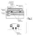
- the impedance difference can be increased considerably, but so doing introduces a large capacitance provided by the bottom electrode and the top metal layer of the mirror. As illustrated in Fig. 1, such capacitance degrades the performance of filters consisting of two or more resonators on a single substrate; the top metallic layer of the mirror creates a capacitance from each bottom electrode to all the other bottom electrodes in a filter, providing a parasitic capacitive coupling between the resonators.
- acoustic-mirror type of resonator in which the acoustic mirror consists of alternating metallic and dielectric layers so as to provide good reflectivity with a relatively small number of layers, but does not introduce capacitive coupling to other resonators formed on the same substrate and using the same acoustic mirror.
- the present invention provides a method of fabricating a multi-resonator bulk acoustic wave (BAW) filter and also a filter provided by such a method, the filter having a plurality of layers of materials serving as an acoustic mirror for a plurality of resonator sections, each resonator section including at least a top electrode and a bottom electrode sandwiching a piezolayer, the method including the steps of: choosing dielectric materials for some of the layers of ma-terials serving as the acoustic mirror and metallic materials for the others of the layers; and providing at least one of the metallic layers via a fabrication procedure in which the metallic layer is patterned into distinct portions by an etching process that removes enough of the metallic layer between where different resonator sections are to be placed as to provide electrical isolation between the portions of the layer beneath the different resonator sections; thereby providing a multi-resonator BAW filter with reduced capacitive coupling between resonators, compared to the capacitive coupling present in a multi-re
- all of the metallic layers are patterned into distinct portions so as to provide electrical isolation between the portions of the all of the layers beneath the different resonator sections.
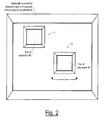
- an acoustic-mirror type multi-resonator BAW filter consists of resonator sections 11 12 situated on top of acoustic mirror layers 14, including metallic layers and dielectric layers, deposited on a substrate 15 so that no metallic mirror layer extends to beneath more than one resonator section.
- acoustic-mirror type multi-resonator BAW filter at least the metallic layers of the acoustic mirror are removed from between the resonator sections. Such selective removal of a deposited material is here called patterning the deposited material.
- a multi-resonator BAW filter including an acoustic mirror, having metallic layers and dielectric layers, in which at least the metallic layers are patterned.
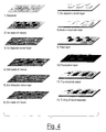
- one method is to deposit in turn the successive layers making up the acoustic mirror, and in so doing, after depositing each metallic layer, to selectively remove it from between each region where a resonator section will be built up before depositing the next dielectric layer.
- the deposition of the metals is usually done by sputtering.
- the dielectric layers can be grown for example by Chemical Vapor Deposition (CVD) or Plasma Enhanced CVD.
- the selective removal (called here patterning ) of the metallic layers can be done by either wet or dry etching.
- the resulting layer stack for one resonator is shown schematically in Fig. 3.
- the preferred materials are SiO2 or Si3N4, and the preferred materials for the metallic (high impedance) layers are W or Mo, although other materials can also be used.
- the piezolayer When the piezolayer is deposited, it extends across the entire face of the substrate (on top of the layers already deposited).
- the piezolayer can either be left unpatterned (not selectively removed), for example when fabricating a two-stage balanced filter (except for providing for vias, i.e. holes in a dielectric layer created by patterning the layer so that when a metal is then deposited on the dielectric layer it will fill the hole, thus providing a connection through the dielectric layer), or the piezolayer can be removed everywhere except on top of each mirror stack.
- the second method of fabricating a multi-resonator BAW filter with an acoustic mirror having patterned metallic layers is to first deposit all the mirror layers and then etch through all the layers to the substrate surface, thereby patterning (selectively removing) not only the metallic layers between each resonator section, but also the dielectric layers.
- the substrate between resonators is then left bare, and there is a large step from the substrate surface to the top of the mirror. Because of the large step, the entire structure of individual acoustic mirrors sitting on top of a bare substrate should be planarized, i.e.
- a thick layer of some dielectric material such as SiO2 or Si3N4 should be deposited over the structure and then polished by for example Chemical Mechanical Polishing (CMP) down to the top of the mirror stacks.
- CMP Chemical Mechanical Polishing
- the electrodes and the piezolayer are deposited on the polished structure, according to the location of each embedded acoustic mirror.
- the second method can be modified by etching and planarizing the mirror stack before depositing the last dielectric mirror layer.
- Such a modification makes it easier to determine when to stop polishing (which in such a modified procedure would be when the surface of the topmost metallic mirror layer is reached).
- the present invention also comprehends a multi-resonator BAW filter fabricated in such a way as to include a completely separate and distinct acoustic mirror beneath each resonator section (advantageously planarized as described above), as opposed to the construction indicated in Fig. 4, in which each dielectric layer in the acoustic mirror material beneath one resonator section is deposited over the entire face of the substrate so as to extend beneath every other resonator section.
- the inventors have discovered that by fabricating a multi-resonator BAW filter according to the invention, there is an improvement (reduced response) in the frequency response of the filter not only away from the center frequency, but there is also an improvement in the response at or near the center frequency.
- a filter according to the prior art will sometimes exhibit a response at or near the center frequency that is highly irregular (i.e. having a deep notch) as a result of the above-described parasitic capacitances
- the response of a filter according to the invention is that of a relatively well-behaved band-pass filter, with a response away from the center frequency that is as much as 6 dB below that of a filter according to the prior art.
- notching near the center frequency of an acoustic mirror type multi-resonator filter can be avoided by taking steps that do not include patterning the metallic layers of the acoustic mirror as in the invention, such steps often result in a reduced bandwidth for the filter. No such bandwidth reduction occurs in the case of fabricating a filter according to the present invention.
Landscapes
- Physics & Mathematics (AREA)
- Acoustics & Sound (AREA)
- Engineering & Computer Science (AREA)
- Manufacturing & Machinery (AREA)
- Chemical & Material Sciences (AREA)
- Crystallography & Structural Chemistry (AREA)
- Piezo-Electric Or Mechanical Vibrators, Or Delay Or Filter Circuits (AREA)
- Headphones And Earphones (AREA)
- Aerials With Secondary Devices (AREA)
Abstract
Description
Claims (8)
- A method of fabricating a multi-resonator bulk acoustic wave (BAW) filter having a plurality of layers of materials serving as an acoustic mirror for a plurality of resonator sections, each resonator section including at least a top electrode and a bottom electrode sandwiching a piezolayer, the method comprising the steps of:thereby providing a multi-resonator BAW filter with reduced capacitive coupling between resonators, compared to the capacitive coupling present in a multi-resonator BAW filter fashioned in a similar manner except excluding the step of etching to pattern any metallic layers of the similarly fashioned acoustic mirror.a) choosing dielectric materials for some of the layers of materials serving as the acoustic mirror and metallic materials for the others of the layers; andb) providing at least one of the metallic layers via a fabrication procedure in which the metallic layer is patterned into distinct portions by an etching process that removes enough of the metallic layer between where different resonator sections are to be placed as to provide electrical isolation between the portions of the layer beneath the different resonator sections;
- A method as in claim 1, wherein all of the metallic layers of the acoustic mirror are patterned into distinct portions by an etching process that removes enough of the metallic layers between where different resonator sections are to be placed as to provide electrical isolation between all of the portions of the layers beneath the different resonator sections.
- A method as in claim 1, wherein step (b) comprises the step of depositing consecutively the different layers of the acoustic mirror, with the dielectric layers alternating with the metallic layers and with the layer nearest the resonator being a dielectric, wherein each metallic layer is patterned as in step (b) before depositing the next dielectric layer.
- A method as in claim 1, wherein step (b) comprises the steps of:a) depositing consecutively all of the different layers of the acoustic mirror, beginning with a metallic layer, so that the dielectric layers alternate with the metallic layers;b) etching through all of the layers of the acoustic mirror, down to the substrate surface, so as to leave on the substrate a pillbox-type structure of the different layers of the acoustic mirror, thereby providing patterned metallic layers and dielectric layers; andc) depositing as a filler a dielectric material on the substrate to replace the material removed from the acoustic mirror layers, the depositing being sufficient in depth to allow polishing the filler down to the top layer of the acoustic mirror.
- A method as in claim 1, wherein step (b) comprises the steps of:a) depositing consecutively the different layers of the acoustic mirror, beginning with a metallic layer and continuing up to but not including the layer that is to be nearest the resonator, so that the dielectric layers alternate with the metallic layers;b) etching through all of the deposited layers of the acoustic mirror, down to the substrate surface, so as to leave on the substrate a pillbox-type structure of the different deposited layers of the acoustic mirror, thereby providing patterned metallic layers and patterned dielectric layers;c) depositing as a filler a dielectric material on the substrate to replace the material removed from the acoustic mirror layers, the depositing being sufficient in depth to allow polishing the filler down to the top deposited layer of the acoustic mirror; andd) depositing the top layer of the acoustic mirror so as to cover not only the already deposited, patterned layers of the acoustic material, but also the filler.
- A method as in claim 1, wherein at least one of the resonator sections is a stacked crystal structure including a top electrode, a middle electrode that is sometimes grounded, and a bottom electrode, and also including two piezolayers sandwiched between the three electrodes.
- A multi-resonator bulk acoustic wave (BAW) filter having a plurality of layers of materials serving as an acoustic mirror for a plurality of resonator sections, each resonator section including at least a top electrode and a bottom electrode sandwiching a piezolayer, wherein some of the layers of the acoustic mirror are fabricated from dielectric materials and others from metallic materials, and further wherein at least one of the metallic layers is patterned into distinct portions by an etching process that removes enough of the metallic layer between where different resonator sections are to be placed as to provide electrical isolation between the portions of the layer beneath the different resonator sections.
- A BAW filter as in claim 7, wherein all of the metallic layers are patterned into distinct portions by an etching process that removes enough of the metallic layers between where different resonator sections are to be placed as to provide electrical isolation between all of the portions of the layers beneath the different resonator sections.
Applications Claiming Priority (2)
| Application Number | Priority Date | Filing Date | Title |
|---|---|---|---|
| US753214 | 2001-01-02 | ||
| US09/753,214 US6496085B2 (en) | 2001-01-02 | 2001-01-02 | Solidly mounted multi-resonator bulk acoustic wave filter with a patterned acoustic mirror |
Publications (4)
| Publication Number | Publication Date |
|---|---|
| EP1227582A2 true EP1227582A2 (en) | 2002-07-31 |
| EP1227582A3 EP1227582A3 (en) | 2004-09-22 |
| EP1227582B1 EP1227582B1 (en) | 2008-07-02 |
| EP1227582B8 EP1227582B8 (en) | 2008-08-13 |
Family
ID=25029665
Family Applications (1)
| Application Number | Title | Priority Date | Filing Date |
|---|---|---|---|
| EP01310923A Expired - Lifetime EP1227582B8 (en) | 2001-01-02 | 2001-12-28 | Solidly mounted multiresonator bulk acoustic wave filter with a patterned acoustic mirror |
Country Status (6)
| Country | Link |
|---|---|
| US (1) | US6496085B2 (en) |
| EP (1) | EP1227582B8 (en) |
| JP (2) | JP4248177B2 (en) |
| CN (1) | CN1208898C (en) |
| AT (1) | ATE400084T1 (en) |
| DE (1) | DE60134621D1 (en) |
Cited By (3)
| Publication number | Priority date | Publication date | Assignee | Title |
|---|---|---|---|---|
| DE102006023165A1 (en) * | 2006-05-17 | 2007-11-22 | Infineon Technologies Ag | Method for producing an acoustic mirror from alternately arranged layers of high and low acoustic impedance |
| WO2009043370A1 (en) * | 2007-10-01 | 2009-04-09 | Telefonaktiebolaget Lm Ericsson (Publ) | A voltage controlled switching device |
| US7616079B2 (en) | 2002-10-08 | 2009-11-10 | Epcos Ag | Bulk acoustic wave resonator and circuit comprising same |
Families Citing this family (71)
| Publication number | Priority date | Publication date | Assignee | Title |
|---|---|---|---|---|
| JP3903848B2 (en) * | 2001-07-02 | 2007-04-11 | 株式会社村田製作所 | Piezoelectric resonator, method for manufacturing piezoelectric resonator, piezoelectric filter, method for manufacturing piezoelectric filter, duplexer, and electronic communication device |
| JP2003229743A (en) * | 2001-11-29 | 2003-08-15 | Murata Mfg Co Ltd | Piezoelectric filter, communication device, and method of manufacturing piezoelectric filter |
| US20100107389A1 (en) * | 2002-01-11 | 2010-05-06 | Avago Technologies Wireless Ip (Singapore) Pte. Ltd. | Method of fabricating an electrode for a bulk acoustic resonator |
| DE10200741A1 (en) * | 2002-01-11 | 2003-07-24 | Infineon Technologies Ag | Process for the production of a topology-optimized electrode for a resonator using thin-film technology |
| US20060043507A1 (en) * | 2002-09-12 | 2006-03-02 | Hans Lobl | Bulk acoustic wave resonator with means for suppression of pass-band ripple in bulk acoustic wave filters |
| DE10258422A1 (en) | 2002-12-13 | 2004-06-24 | Epcos Ag | Bulk acoustic wave device for filter in mobile telecommunications terminal, has resonators arranged on acoustic reflector and electrically connected so that coupling capacitance does not shunt them |
| DE10301261B4 (en) * | 2003-01-15 | 2018-03-22 | Snaptrack, Inc. | Bulk acoustic wave device and method of manufacture |
| US7275292B2 (en) * | 2003-03-07 | 2007-10-02 | Avago Technologies Wireless Ip (Singapore) Pte. Ltd. | Method for fabricating an acoustical resonator on a substrate |
| JP3945486B2 (en) * | 2004-02-18 | 2007-07-18 | ソニー株式会社 | Thin film bulk acoustic resonator and manufacturing method thereof |
| KR100622955B1 (en) * | 2004-04-06 | 2006-09-18 | 삼성전자주식회사 | Thin film bulk acoustic resonator and its manufacturing method |
| US7388454B2 (en) | 2004-10-01 | 2008-06-17 | Avago Technologies Wireless Ip Pte Ltd | Acoustic resonator performance enhancement using alternating frame structure |
| DE102004054895B4 (en) * | 2004-11-12 | 2007-04-19 | Infineon Technologies Ag | Thin-film BAW filter and method for producing a thin-film BAW filter |
| US8981876B2 (en) | 2004-11-15 | 2015-03-17 | Avago Technologies General Ip (Singapore) Pte. Ltd. | Piezoelectric resonator structures and electrical filters having frame elements |
| US7202560B2 (en) | 2004-12-15 | 2007-04-10 | Avago Technologies Wireless Ip (Singapore) Pte. Ltd. | Wafer bonding of micro-electro mechanical systems to active circuitry |
| US7791434B2 (en) | 2004-12-22 | 2010-09-07 | Avago Technologies Wireless Ip (Singapore) Pte. Ltd. | Acoustic resonator performance enhancement using selective metal etch and having a trench in the piezoelectric |
| US7369013B2 (en) | 2005-04-06 | 2008-05-06 | Avago Technologies Wireless Ip Pte Ltd | Acoustic resonator performance enhancement using filled recessed region |
| FR2889374A1 (en) * | 2005-07-29 | 2007-02-02 | Michelin Soc Tech | HYBRID RESONANT STRUCTURE FOR VERIFYING PARAMETERS OF A TIRE |
| US7675390B2 (en) | 2005-10-18 | 2010-03-09 | Avago Technologies Wireless Ip (Singapore) Pte. Ltd. | Acoustic galvanic isolator incorporating single decoupled stacked bulk acoustic resonator |
| US7737807B2 (en) | 2005-10-18 | 2010-06-15 | Avago Technologies Wireless Ip (Singapore) Pte. Ltd. | Acoustic galvanic isolator incorporating series-connected decoupled stacked bulk acoustic resonators |
| US7463499B2 (en) | 2005-10-31 | 2008-12-09 | Avago Technologies General Ip (Singapore) Pte Ltd. | AC-DC power converter |
| JP2007129391A (en) * | 2005-11-02 | 2007-05-24 | Matsushita Electric Ind Co Ltd | Acoustic resonator and filter |
| US7544612B1 (en) | 2006-01-20 | 2009-06-09 | Skyworks Solutions, Inc. | Method and structure for reducing the effect of vertical steps in patterned layers in semiconductor structures |
| US7612636B2 (en) | 2006-01-30 | 2009-11-03 | Avago Technologies Wireless Ip (Singapore) Pte. Ltd. | Impedance transforming bulk acoustic wave baluns |
| US7414350B1 (en) * | 2006-03-03 | 2008-08-19 | Skyworks Solutions, Inc. | Acoustic mirror structure for a bulk acoustic wave structure and method for fabricating same |
| US7746677B2 (en) | 2006-03-09 | 2010-06-29 | Avago Technologies Wireless Ip (Singapore) Pte. Ltd. | AC-DC converter circuit and power supply |
| US7479685B2 (en) | 2006-03-10 | 2009-01-20 | Avago Technologies General Ip (Singapore) Pte. Ltd. | Electronic device on substrate with cavity and mitigated parasitic leakage path |
| JP4525623B2 (en) * | 2006-03-23 | 2010-08-18 | エプソントヨコム株式会社 | Method for manufacturing piezoelectric vibrating piece |
| JP4846477B2 (en) * | 2006-07-26 | 2011-12-28 | パナソニック株式会社 | Method for manufacturing thin film acoustic resonator |
| JP5096695B2 (en) * | 2006-05-30 | 2012-12-12 | パナソニック株式会社 | Thin film acoustic resonator |
| JP2008172713A (en) * | 2007-01-15 | 2008-07-24 | Hitachi Media Electoronics Co Ltd | Piezoelectric thin film resonator, piezoelectric thin film resonator filter, and manufacturing method thereof |
| US8188548B2 (en) * | 2007-02-15 | 2012-05-29 | Infineon Technologies Ag | Device and method for reducing a voltage dependent capacitive coupling |
| WO2009008973A2 (en) * | 2007-07-11 | 2009-01-15 | Skyworks Solutions, Inc. | Method for forming an acoustic mirror with reduced metal layer roughness and related structure |
| US20090053401A1 (en) * | 2007-08-24 | 2009-02-26 | Maxim Integrated Products, Inc. | Piezoelectric deposition for BAW resonators |
| JP4930595B2 (en) * | 2007-09-06 | 2012-05-16 | 株式会社村田製作所 | Piezoelectric resonator |
| US7791435B2 (en) | 2007-09-28 | 2010-09-07 | Avago Technologies Wireless Ip (Singapore) Pte. Ltd. | Single stack coupled resonators having differential output |
| US8514033B2 (en) * | 2007-10-18 | 2013-08-20 | Avago Technologies General Ip (Singapore) Pte. Ltd. | BAW structure with reduced topographic steps and related method |
| US8512800B2 (en) * | 2007-12-04 | 2013-08-20 | Triquint Semiconductor, Inc. | Optimal acoustic impedance materials for polished substrate coating to suppress passband ripple in BAW resonators and filters |
| US7732977B2 (en) | 2008-04-30 | 2010-06-08 | Avago Technologies Wireless Ip (Singapore) | Transceiver circuit for film bulk acoustic resonator (FBAR) transducers |
| US7855618B2 (en) | 2008-04-30 | 2010-12-21 | Avago Technologies Wireless Ip (Singapore) Pte. Ltd. | Bulk acoustic resonator electrical impedance transformers |
| US7768364B2 (en) * | 2008-06-09 | 2010-08-03 | Maxim Integrated Products, Inc. | Bulk acoustic resonators with multi-layer electrodes |
| US8902023B2 (en) | 2009-06-24 | 2014-12-02 | Avago Technologies General Ip (Singapore) Pte. Ltd. | Acoustic resonator structure having an electrode with a cantilevered portion |
| US8248185B2 (en) | 2009-06-24 | 2012-08-21 | Avago Technologies Wireless Ip (Singapore) Pte. Ltd. | Acoustic resonator structure comprising a bridge |
| JP5113870B2 (en) * | 2009-08-27 | 2013-01-09 | 日本電波工業株式会社 | Manufacturing method of surface mount crystal unit |
| US8193877B2 (en) | 2009-11-30 | 2012-06-05 | Avago Technologies Wireless Ip (Singapore) Pte. Ltd. | Duplexer with negative phase shifting circuit |
| US8796904B2 (en) | 2011-10-31 | 2014-08-05 | Avago Technologies General Ip (Singapore) Pte. Ltd. | Bulk acoustic resonator comprising piezoelectric layer and inverse piezoelectric layer |
| US9243316B2 (en) | 2010-01-22 | 2016-01-26 | Avago Technologies General Ip (Singapore) Pte. Ltd. | Method of fabricating piezoelectric material with selected c-axis orientation |
| US8962443B2 (en) | 2011-01-31 | 2015-02-24 | Avago Technologies General Ip (Singapore) Pte. Ltd. | Semiconductor device having an airbridge and method of fabricating the same |
| US9203374B2 (en) | 2011-02-28 | 2015-12-01 | Avago Technologies General Ip (Singapore) Pte. Ltd. | Film bulk acoustic resonator comprising a bridge |
| US9148117B2 (en) | 2011-02-28 | 2015-09-29 | Avago Technologies General Ip (Singapore) Pte. Ltd. | Coupled resonator filter comprising a bridge and frame elements |
| US9425764B2 (en) | 2012-10-25 | 2016-08-23 | Avago Technologies General Ip (Singapore) Pte. Ltd. | Accoustic resonator having composite electrodes with integrated lateral features |
| US9154112B2 (en) | 2011-02-28 | 2015-10-06 | Avago Technologies General Ip (Singapore) Pte. Ltd. | Coupled resonator filter comprising a bridge |
| US9083302B2 (en) | 2011-02-28 | 2015-07-14 | Avago Technologies General Ip (Singapore) Pte. Ltd. | Stacked bulk acoustic resonator comprising a bridge and an acoustic reflector along a perimeter of the resonator |
| US9136818B2 (en) | 2011-02-28 | 2015-09-15 | Avago Technologies General Ip (Singapore) Pte. Ltd. | Stacked acoustic resonator comprising a bridge |
| US9048812B2 (en) | 2011-02-28 | 2015-06-02 | Avago Technologies General Ip (Singapore) Pte. Ltd. | Bulk acoustic wave resonator comprising bridge formed within piezoelectric layer |
| US8575820B2 (en) | 2011-03-29 | 2013-11-05 | Avago Technologies General Ip (Singapore) Pte. Ltd. | Stacked bulk acoustic resonator |
| US9444426B2 (en) | 2012-10-25 | 2016-09-13 | Avago Technologies General Ip (Singapore) Pte. Ltd. | Accoustic resonator having integrated lateral feature and temperature compensation feature |
| US8350445B1 (en) | 2011-06-16 | 2013-01-08 | Avago Technologies Wireless Ip (Singapore) Pte. Ltd. | Bulk acoustic resonator comprising non-piezoelectric layer and bridge |
| US8922302B2 (en) | 2011-08-24 | 2014-12-30 | Avago Technologies General Ip (Singapore) Pte. Ltd. | Acoustic resonator formed on a pedestal |
| WO2016147986A1 (en) * | 2015-03-16 | 2016-09-22 | 株式会社村田製作所 | Elastic wave device and production method for same |
| US9602076B1 (en) * | 2015-05-19 | 2017-03-21 | Qorvo Us, Inc. | Resonators with balancing capacitor |
| US10581403B2 (en) | 2016-07-11 | 2020-03-03 | Qorvo Us, Inc. | Device having a titanium-alloyed surface |
| US10361676B2 (en) * | 2017-09-29 | 2019-07-23 | Qorvo Us, Inc. | Baw filter structure with internal electrostatic shielding |
| KR102722507B1 (en) * | 2017-12-07 | 2024-10-29 | 인피니언 테크놀로지스 아게 | Acoustically coupled resonator notch and bandpass filters |
| US11757430B2 (en) | 2020-01-07 | 2023-09-12 | Qorvo Us, Inc. | Acoustic filter circuit for noise suppression outside resonance frequency |
| US11632097B2 (en) | 2020-11-04 | 2023-04-18 | Qorvo Us, Inc. | Coupled resonator filter device |
| US11575363B2 (en) | 2021-01-19 | 2023-02-07 | Qorvo Us, Inc. | Hybrid bulk acoustic wave filter |
| CN112953449B (en) * | 2021-03-04 | 2024-10-01 | 偲百创(深圳)科技有限公司 | Method for manufacturing an acoustic resonator with transversely excited shear mode |
| CN114285390B (en) * | 2021-03-15 | 2025-11-18 | 偲百创(深圳)科技有限公司 | Acoustic resonators with thickness-direction excitation shear mode |
| JP7794615B2 (en) * | 2021-11-29 | 2026-01-06 | 太陽誘電株式会社 | Piezoelectric thin film resonator and its manufacturing method |
| US12170515B2 (en) | 2022-01-31 | 2024-12-17 | Qorvo Us, Inc. | Reversed semilattice filter |
| US12587172B2 (en) | 2023-03-15 | 2026-03-24 | Qorvo Us, Inc. | Pin reconfigurable baw filters |
Family Cites Families (14)
| Publication number | Priority date | Publication date | Assignee | Title |
|---|---|---|---|---|
| JPH07114340B2 (en) * | 1987-01-19 | 1995-12-06 | 株式会社東芝 | Piezoelectric thin film resonator |
| JPS63187713A (en) * | 1987-01-29 | 1988-08-03 | Toshiba Corp | Integrated piezoelectric thin film function element |
| US5864261A (en) * | 1994-05-23 | 1999-01-26 | Iowa State University Research Foundation | Multiple layer acoustical structures for thin-film resonator based circuits and systems |
| JPH08186467A (en) * | 1994-12-29 | 1996-07-16 | Murata Mfg Co Ltd | Divergent oscillation type piezoelectric oscillator and its production |
| US5821833A (en) * | 1995-12-26 | 1998-10-13 | Tfr Technologies, Inc. | Stacked crystal filter device and method of making |
| US5714917A (en) | 1996-10-02 | 1998-02-03 | Nokia Mobile Phones Limited | Device incorporating a tunable thin film bulk acoustic resonator for performing amplitude and phase modulation |
| US5873154A (en) | 1996-10-17 | 1999-02-23 | Nokia Mobile Phones Limited | Method for fabricating a resonator having an acoustic mirror |
| US5872493A (en) * | 1997-03-13 | 1999-02-16 | Nokia Mobile Phones, Ltd. | Bulk acoustic wave (BAW) filter having a top portion that includes a protective acoustic mirror |
| AU2712597A (en) * | 1997-05-13 | 1998-12-08 | Mitsubishi Denki Kabushiki Kaisha | Piezoelectric thin film device |
| US5910756A (en) * | 1997-05-21 | 1999-06-08 | Nokia Mobile Phones Limited | Filters and duplexers utilizing thin film stacked crystal filter structures and thin film bulk acoustic wave resonators |
| FI108583B (en) * | 1998-06-02 | 2002-02-15 | Nokia Corp | resonator structures |
| US6060818A (en) | 1998-06-02 | 2000-05-09 | Hewlett-Packard Company | SBAR structures and method of fabrication of SBAR.FBAR film processing techniques for the manufacturing of SBAR/BAR filters |
| ATE284091T1 (en) * | 1998-09-11 | 2004-12-15 | Texas Instruments Inc | INTEGRATED ACOUSTIC THIN FILM RESONATOR |
| FI113211B (en) * | 1998-12-30 | 2004-03-15 | Nokia Corp | Balanced filter construction and telecommunication apparatus |
-
2001
- 2001-01-02 US US09/753,214 patent/US6496085B2/en not_active Expired - Lifetime
- 2001-12-20 JP JP2001388031A patent/JP4248177B2/en not_active Expired - Lifetime
- 2001-12-28 AT AT01310923T patent/ATE400084T1/en not_active IP Right Cessation
- 2001-12-28 EP EP01310923A patent/EP1227582B8/en not_active Expired - Lifetime
- 2001-12-28 DE DE60134621T patent/DE60134621D1/en not_active Expired - Lifetime
- 2001-12-31 CN CNB011395990A patent/CN1208898C/en not_active Expired - Lifetime
-
2008
- 2008-10-17 JP JP2008268710A patent/JP4838292B2/en not_active Expired - Fee Related
Cited By (6)
| Publication number | Priority date | Publication date | Assignee | Title |
|---|---|---|---|---|
| US7616079B2 (en) | 2002-10-08 | 2009-11-10 | Epcos Ag | Bulk acoustic wave resonator and circuit comprising same |
| DE102006023165A1 (en) * | 2006-05-17 | 2007-11-22 | Infineon Technologies Ag | Method for producing an acoustic mirror from alternately arranged layers of high and low acoustic impedance |
| DE102006023165B4 (en) * | 2006-05-17 | 2008-02-14 | Infineon Technologies Ag | Method for producing an acoustic mirror from alternately arranged layers of high and low acoustic impedance |
| US7669310B2 (en) | 2006-05-17 | 2010-03-02 | Avago Technologies Wireless Ip (Singapore) Pte. Ltd. | Method of manufacturing an acoustic mirror |
| US8256093B2 (en) | 2006-05-17 | 2012-09-04 | Avago Technologies Wireless Ip (Singapore) Pte. Ltd. | Method of manufacturing an acoustic mirror |
| WO2009043370A1 (en) * | 2007-10-01 | 2009-04-09 | Telefonaktiebolaget Lm Ericsson (Publ) | A voltage controlled switching device |
Also Published As
| Publication number | Publication date |
|---|---|
| US20020084873A1 (en) | 2002-07-04 |
| JP2002251190A (en) | 2002-09-06 |
| EP1227582B1 (en) | 2008-07-02 |
| ATE400084T1 (en) | 2008-07-15 |
| JP2009022052A (en) | 2009-01-29 |
| JP4838292B2 (en) | 2011-12-14 |
| DE60134621D1 (en) | 2008-08-14 |
| US6496085B2 (en) | 2002-12-17 |
| CN1208898C (en) | 2005-06-29 |
| CN1365186A (en) | 2002-08-21 |
| EP1227582A3 (en) | 2004-09-22 |
| EP1227582B8 (en) | 2008-08-13 |
| JP4248177B2 (en) | 2009-04-02 |
Similar Documents
| Publication | Publication Date | Title |
|---|---|---|
| US6496085B2 (en) | Solidly mounted multi-resonator bulk acoustic wave filter with a patterned acoustic mirror | |
| JP4113637B2 (en) | Acoustic resonator and manufacturing method | |
| US6601276B2 (en) | Method for self alignment of patterned layers in thin film acoustic devices | |
| US7128941B2 (en) | Method for fabricating film bulk acoustic resonator (FBAR) device | |
| EP1471637B1 (en) | Method for fabricating cantilevered type film bulk acoustic resonator and film bulk acoustic resonator fabricated by the same | |
| JP4318653B2 (en) | Bulk acoustic wave filter and method for removing unwanted sideband passband | |
| KR100398363B1 (en) | Film bulk acoustic resonator and method for fabrication thereof | |
| US6518860B2 (en) | BAW filters having different center frequencies on a single substrate and a method for providing same | |
| US6774746B2 (en) | Thin film bulk acoustic resonator filters with a piezoelectric layer of lead scandium tantalum oxide | |
| US7138889B2 (en) | Single-port multi-resonator acoustic resonator device | |
| US9450563B2 (en) | Acoustic wave bandpass filter comprising integrated acoustic guiding | |
| CN104716925B (en) | Piezoelectric thin film vibrator and its manufacture method, wave filter and duplexer | |
| JP2003505906A (en) | Resonator structure and filter having the resonator structure | |
| KR20110058704A (en) | Hybrid Bulk Acoustic Resonator and Manufacturing Method Thereof | |
| WO2007119643A1 (en) | Film bulk acoustic resonator, piezoelectric thin film device and method for manufacturing the piezoelectric thin film device | |
| JP2007028669A (en) | Method for manufacturing thin film acoustic resonator | |
| JP2008182543A (en) | Thin film piezoelectric resonator and thin film piezoelectric filter using the same | |
| US7046103B2 (en) | Electric filter comprising a plurality of thin film bulk acoustic resonators | |
| JP2005303573A (en) | Thin film piezoelectric resonator and manufacturing method thereof | |
| JP3918464B2 (en) | Thin film acoustic resonator and manufacturing method thereof | |
| CN121239178A (en) | Thin film bulk acoustic resonator and filter |
Legal Events
| Date | Code | Title | Description |
|---|---|---|---|
| PUAI | Public reference made under article 153(3) epc to a published international application that has entered the european phase |
Free format text: ORIGINAL CODE: 0009012 |
|
| AK | Designated contracting states |
Kind code of ref document: A2 Designated state(s): AT BE CH CY DE DK ES FI FR GB GR IE IT LI LU MC NL PT SE TR |
|
| AX | Request for extension of the european patent |
Free format text: AL;LT;LV;MK;RO;SI |
|
| PUAL | Search report despatched |
Free format text: ORIGINAL CODE: 0009013 |
|
| AK | Designated contracting states |
Kind code of ref document: A3 Designated state(s): AT BE CH CY DE DK ES FI FR GB GR IE IT LI LU MC NL PT SE TR |
|
| AX | Request for extension of the european patent |
Extension state: AL LT LV MK RO SI |
|
| 17P | Request for examination filed |
Effective date: 20050216 |
|
| AKX | Designation fees paid |
Designated state(s): AT BE CH CY DE DK ES FI FR GB GR IE IT LI LU MC NL PT SE TR |
|
| 17Q | First examination report despatched |
Effective date: 20070413 |
|
| GRAP | Despatch of communication of intention to grant a patent |
Free format text: ORIGINAL CODE: EPIDOSNIGR1 |
|
| GRAS | Grant fee paid |
Free format text: ORIGINAL CODE: EPIDOSNIGR3 |
|
| GRAA | (expected) grant |
Free format text: ORIGINAL CODE: 0009210 |
|
| AK | Designated contracting states |
Kind code of ref document: B1 Designated state(s): AT BE CH CY DE DK ES FI FR GB GR IE IT LI LU MC NL PT SE TR |
|
| REG | Reference to a national code |
Ref country code: GB Ref legal event code: FG4D |
|
| RAP2 | Party data changed (patent owner data changed or rights of a patent transferred) |
Owner name: AVAGO TECHNOLOGIES WIRELESS IP (SINGAPORE) PTE. LT |
|
| REG | Reference to a national code |
Ref country code: CH Ref legal event code: EP |
|
| REF | Corresponds to: |
Ref document number: 60134621 Country of ref document: DE Date of ref document: 20080814 Kind code of ref document: P |
|
| REG | Reference to a national code |
Ref country code: IE Ref legal event code: FG4D |
|
| NLT2 | Nl: modifications (of names), taken from the european patent patent bulletin |
Owner name: AVAGO TECHNOLOGIES WIRELESS IP Effective date: 20080730 |
|
| PG25 | Lapsed in a contracting state [announced via postgrant information from national office to epo] |
Ref country code: NL Free format text: LAPSE BECAUSE OF FAILURE TO SUBMIT A TRANSLATION OF THE DESCRIPTION OR TO PAY THE FEE WITHIN THE PRESCRIBED TIME-LIMIT Effective date: 20080702 |
|
| NLV1 | Nl: lapsed or annulled due to failure to fulfill the requirements of art. 29p and 29m of the patents act | ||
| PG25 | Lapsed in a contracting state [announced via postgrant information from national office to epo] |
Ref country code: PT Free format text: LAPSE BECAUSE OF FAILURE TO SUBMIT A TRANSLATION OF THE DESCRIPTION OR TO PAY THE FEE WITHIN THE PRESCRIBED TIME-LIMIT Effective date: 20081202 Ref country code: ES Free format text: LAPSE BECAUSE OF FAILURE TO SUBMIT A TRANSLATION OF THE DESCRIPTION OR TO PAY THE FEE WITHIN THE PRESCRIBED TIME-LIMIT Effective date: 20081013 |
|
| PG25 | Lapsed in a contracting state [announced via postgrant information from national office to epo] |
Ref country code: FI Free format text: LAPSE BECAUSE OF FAILURE TO SUBMIT A TRANSLATION OF THE DESCRIPTION OR TO PAY THE FEE WITHIN THE PRESCRIBED TIME-LIMIT Effective date: 20080702 Ref country code: AT Free format text: LAPSE BECAUSE OF FAILURE TO SUBMIT A TRANSLATION OF THE DESCRIPTION OR TO PAY THE FEE WITHIN THE PRESCRIBED TIME-LIMIT Effective date: 20080702 |
|
| PG25 | Lapsed in a contracting state [announced via postgrant information from national office to epo] |
Ref country code: BE Free format text: LAPSE BECAUSE OF FAILURE TO SUBMIT A TRANSLATION OF THE DESCRIPTION OR TO PAY THE FEE WITHIN THE PRESCRIBED TIME-LIMIT Effective date: 20080702 |
|
| PG25 | Lapsed in a contracting state [announced via postgrant information from national office to epo] |
Ref country code: DK Free format text: LAPSE BECAUSE OF FAILURE TO SUBMIT A TRANSLATION OF THE DESCRIPTION OR TO PAY THE FEE WITHIN THE PRESCRIBED TIME-LIMIT Effective date: 20080702 |
|
| PLBE | No opposition filed within time limit |
Free format text: ORIGINAL CODE: 0009261 |
|
| STAA | Information on the status of an ep patent application or granted ep patent |
Free format text: STATUS: NO OPPOSITION FILED WITHIN TIME LIMIT |
|
| 26N | No opposition filed |
Effective date: 20090403 |
|
| PG25 | Lapsed in a contracting state [announced via postgrant information from national office to epo] |
Ref country code: MC Free format text: LAPSE BECAUSE OF NON-PAYMENT OF DUE FEES Effective date: 20081231 |
|
| REG | Reference to a national code |
Ref country code: CH Ref legal event code: PL |
|
| GBPC | Gb: european patent ceased through non-payment of renewal fee |
Effective date: 20081228 |
|
| PG25 | Lapsed in a contracting state [announced via postgrant information from national office to epo] |
Ref country code: IT Free format text: LAPSE BECAUSE OF FAILURE TO SUBMIT A TRANSLATION OF THE DESCRIPTION OR TO PAY THE FEE WITHIN THE PRESCRIBED TIME-LIMIT Effective date: 20080702 |
|
| REG | Reference to a national code |
Ref country code: FR Ref legal event code: ST Effective date: 20090831 |
|
| REG | Reference to a national code |
Ref country code: IE Ref legal event code: MM4A |
|
| PG25 | Lapsed in a contracting state [announced via postgrant information from national office to epo] |
Ref country code: LI Free format text: LAPSE BECAUSE OF NON-PAYMENT OF DUE FEES Effective date: 20081231 Ref country code: CH Free format text: LAPSE BECAUSE OF NON-PAYMENT OF DUE FEES Effective date: 20081231 |
|
| PG25 | Lapsed in a contracting state [announced via postgrant information from national office to epo] |
Ref country code: GB Free format text: LAPSE BECAUSE OF NON-PAYMENT OF DUE FEES Effective date: 20081228 |
|
| PG25 | Lapsed in a contracting state [announced via postgrant information from national office to epo] |
Ref country code: SE Free format text: LAPSE BECAUSE OF FAILURE TO SUBMIT A TRANSLATION OF THE DESCRIPTION OR TO PAY THE FEE WITHIN THE PRESCRIBED TIME-LIMIT Effective date: 20081002 Ref country code: IE Free format text: LAPSE BECAUSE OF NON-PAYMENT OF DUE FEES Effective date: 20081228 |
|
| PG25 | Lapsed in a contracting state [announced via postgrant information from national office to epo] |
Ref country code: FR Free format text: LAPSE BECAUSE OF NON-PAYMENT OF DUE FEES Effective date: 20081231 |
|
| PG25 | Lapsed in a contracting state [announced via postgrant information from national office to epo] |
Ref country code: LU Free format text: LAPSE BECAUSE OF NON-PAYMENT OF DUE FEES Effective date: 20081228 Ref country code: CY Free format text: LAPSE BECAUSE OF FAILURE TO SUBMIT A TRANSLATION OF THE DESCRIPTION OR TO PAY THE FEE WITHIN THE PRESCRIBED TIME-LIMIT Effective date: 20080702 |
|
| PG25 | Lapsed in a contracting state [announced via postgrant information from national office to epo] |
Ref country code: TR Free format text: LAPSE BECAUSE OF FAILURE TO SUBMIT A TRANSLATION OF THE DESCRIPTION OR TO PAY THE FEE WITHIN THE PRESCRIBED TIME-LIMIT Effective date: 20080702 |
|
| PG25 | Lapsed in a contracting state [announced via postgrant information from national office to epo] |
Ref country code: GR Free format text: LAPSE BECAUSE OF FAILURE TO SUBMIT A TRANSLATION OF THE DESCRIPTION OR TO PAY THE FEE WITHIN THE PRESCRIBED TIME-LIMIT Effective date: 20081003 |
|
| REG | Reference to a national code |
Ref country code: DE Ref legal event code: R081 Ref document number: 60134621 Country of ref document: DE Owner name: AVAGO TECHNOLOGIES GENERAL IP (SINGAPORE) PTE., SG Free format text: FORMER OWNER: AVAGO TECHNOLOGIES WIRELESS IP (SINGAPORE) PTE. LTD., SINGAPORE, SG Effective date: 20130606 Ref country code: DE Ref legal event code: R082 Ref document number: 60134621 Country of ref document: DE Representative=s name: DILG HAEUSLER SCHINDELMANN PATENTANWALTSGESELL, DE Effective date: 20130606 |
|
| REG | Reference to a national code |
Ref country code: DE Ref legal event code: R081 Ref document number: 60134621 Country of ref document: DE Owner name: AVAGO TECHNOLOGIES INTERNATIONAL SALES PTE. LT, SG Free format text: FORMER OWNER: AVAGO TECHNOLOGIES GENERAL IP (SINGAPORE) PTE. LTD., SINGAPORE, SG Ref country code: DE Ref legal event code: R082 Ref document number: 60134621 Country of ref document: DE Representative=s name: DILG, HAEUSLER, SCHINDELMANN PATENTANWALTSGESE, DE Ref country code: DE Ref legal event code: R082 Ref document number: 60134621 Country of ref document: DE Representative=s name: DILG HAEUSLER SCHINDELMANN PATENTANWALTSGESELL, DE |
|
| PGFP | Annual fee paid to national office [announced via postgrant information from national office to epo] |
Ref country code: DE Payment date: 20201210 Year of fee payment: 20 |
|
| REG | Reference to a national code |
Ref country code: DE Ref legal event code: R071 Ref document number: 60134621 Country of ref document: DE |