EP1227361A2 - Semiconductor optical device having reduced parasitic capacitance - Google Patents
Semiconductor optical device having reduced parasitic capacitance Download PDFInfo
- Publication number
- EP1227361A2 EP1227361A2 EP01120900A EP01120900A EP1227361A2 EP 1227361 A2 EP1227361 A2 EP 1227361A2 EP 01120900 A EP01120900 A EP 01120900A EP 01120900 A EP01120900 A EP 01120900A EP 1227361 A2 EP1227361 A2 EP 1227361A2
- Authority
- EP
- European Patent Office
- Prior art keywords
- layer
- layers
- mesa stripe
- current blocking
- semiconductor
- Prior art date
- Legal status (The legal status is an assumption and is not a legal conclusion. Google has not performed a legal analysis and makes no representation as to the accuracy of the status listed.)
- Withdrawn
Links
Images


Classifications
-
- G—PHYSICS
- G02—OPTICS
- G02F—OPTICAL DEVICES OR ARRANGEMENTS FOR THE CONTROL OF LIGHT BY MODIFICATION OF THE OPTICAL PROPERTIES OF THE MEDIA OF THE ELEMENTS INVOLVED THEREIN; NON-LINEAR OPTICS; FREQUENCY-CHANGING OF LIGHT; OPTICAL LOGIC ELEMENTS; OPTICAL ANALOGUE/DIGITAL CONVERTERS
- G02F1/00—Devices or arrangements for the control of the intensity, colour, phase, polarisation or direction of light arriving from an independent light source, e.g. switching, gating or modulating; Non-linear optics
- G02F1/01—Devices or arrangements for the control of the intensity, colour, phase, polarisation or direction of light arriving from an independent light source, e.g. switching, gating or modulating; Non-linear optics for the control of the intensity, phase, polarisation or colour
- G02F1/015—Devices or arrangements for the control of the intensity, colour, phase, polarisation or direction of light arriving from an independent light source, e.g. switching, gating or modulating; Non-linear optics for the control of the intensity, phase, polarisation or colour based on semiconductor elements having potential barriers, e.g. having a PN or PIN junction
- G02F1/025—Devices or arrangements for the control of the intensity, colour, phase, polarisation or direction of light arriving from an independent light source, e.g. switching, gating or modulating; Non-linear optics for the control of the intensity, phase, polarisation or colour based on semiconductor elements having potential barriers, e.g. having a PN or PIN junction in an optical waveguide structure
-
- B—PERFORMING OPERATIONS; TRANSPORTING
- B82—NANOTECHNOLOGY
- B82Y—SPECIFIC USES OR APPLICATIONS OF NANOSTRUCTURES; MEASUREMENT OR ANALYSIS OF NANOSTRUCTURES; MANUFACTURE OR TREATMENT OF NANOSTRUCTURES
- B82Y20/00—Nanooptics, e.g. quantum optics or photonic crystals
-
- G—PHYSICS
- G02—OPTICS
- G02F—OPTICAL DEVICES OR ARRANGEMENTS FOR THE CONTROL OF LIGHT BY MODIFICATION OF THE OPTICAL PROPERTIES OF THE MEDIA OF THE ELEMENTS INVOLVED THEREIN; NON-LINEAR OPTICS; FREQUENCY-CHANGING OF LIGHT; OPTICAL LOGIC ELEMENTS; OPTICAL ANALOGUE/DIGITAL CONVERTERS
- G02F1/00—Devices or arrangements for the control of the intensity, colour, phase, polarisation or direction of light arriving from an independent light source, e.g. switching, gating or modulating; Non-linear optics
- G02F1/01—Devices or arrangements for the control of the intensity, colour, phase, polarisation or direction of light arriving from an independent light source, e.g. switching, gating or modulating; Non-linear optics for the control of the intensity, phase, polarisation or colour
- G02F1/015—Devices or arrangements for the control of the intensity, colour, phase, polarisation or direction of light arriving from an independent light source, e.g. switching, gating or modulating; Non-linear optics for the control of the intensity, phase, polarisation or colour based on semiconductor elements having potential barriers, e.g. having a PN or PIN junction
- G02F1/017—Structures with periodic or quasi periodic potential variation, e.g. superlattices, quantum wells
-
- G—PHYSICS
- G02—OPTICS
- G02F—OPTICAL DEVICES OR ARRANGEMENTS FOR THE CONTROL OF LIGHT BY MODIFICATION OF THE OPTICAL PROPERTIES OF THE MEDIA OF THE ELEMENTS INVOLVED THEREIN; NON-LINEAR OPTICS; FREQUENCY-CHANGING OF LIGHT; OPTICAL LOGIC ELEMENTS; OPTICAL ANALOGUE/DIGITAL CONVERTERS
- G02F2201/00—Constructional arrangements not provided for in groups G02F1/00 - G02F7/00
- G02F2201/06—Constructional arrangements not provided for in groups G02F1/00 - G02F7/00 integrated waveguide
- G02F2201/066—Constructional arrangements not provided for in groups G02F1/00 - G02F7/00 integrated waveguide channel; buried
-
- H—ELECTRICITY
- H01—ELECTRIC ELEMENTS
- H01S—DEVICES USING THE PROCESS OF LIGHT AMPLIFICATION BY STIMULATED EMISSION OF RADIATION [LASER] TO AMPLIFY OR GENERATE LIGHT; DEVICES USING STIMULATED EMISSION OF ELECTROMAGNETIC RADIATION IN WAVE RANGES OTHER THAN OPTICAL
- H01S5/00—Semiconductor lasers
- H01S5/02—Structural details or components not essential to laser action
- H01S5/026—Monolithically integrated components, e.g. waveguides, monitoring photo-detectors, drivers
- H01S5/0265—Intensity modulators
-
- H—ELECTRICITY
- H01—ELECTRIC ELEMENTS
- H01S—DEVICES USING THE PROCESS OF LIGHT AMPLIFICATION BY STIMULATED EMISSION OF RADIATION [LASER] TO AMPLIFY OR GENERATE LIGHT; DEVICES USING STIMULATED EMISSION OF ELECTROMAGNETIC RADIATION IN WAVE RANGES OTHER THAN OPTICAL
- H01S5/00—Semiconductor lasers
- H01S5/02—Structural details or components not essential to laser action
- H01S5/028—Coatings ; Treatment of the laser facets, e.g. etching, passivation layers or reflecting layers
- H01S5/0282—Passivation layers or treatments
-
- H—ELECTRICITY
- H01—ELECTRIC ELEMENTS
- H01S—DEVICES USING THE PROCESS OF LIGHT AMPLIFICATION BY STIMULATED EMISSION OF RADIATION [LASER] TO AMPLIFY OR GENERATE LIGHT; DEVICES USING STIMULATED EMISSION OF ELECTROMAGNETIC RADIATION IN WAVE RANGES OTHER THAN OPTICAL
- H01S5/00—Semiconductor lasers
- H01S5/20—Structure or shape of the semiconductor body to guide the optical wave ; Confining structures perpendicular to the optical axis, e.g. index or gain guiding, stripe geometry, broad area lasers, gain tailoring, transverse or lateral reflectors, special cladding structures, MQW barrier reflection layers
- H01S5/22—Structure or shape of the semiconductor body to guide the optical wave ; Confining structures perpendicular to the optical axis, e.g. index or gain guiding, stripe geometry, broad area lasers, gain tailoring, transverse or lateral reflectors, special cladding structures, MQW barrier reflection layers having a ridge or stripe structure
- H01S5/227—Buried mesa structure ; Striped active layer
- H01S5/2275—Buried mesa structure ; Striped active layer mesa created by etching
Definitions
- the present invention relates to a semiconductor optical device having a reduced parasitic capacitance and, more particularly, to a semiconductor optical device suited for use as a semiconductor optical modulator.
- the present invention also relates to a method for manufacturing the same.
- Semiconductor optical modulators are widely used in the field of optical communication for transmitting optical signals.
- the semiconductor optical modulator is used for optical intensity modulation or optical frequency modulation to transmit an optical signal light, which modulates a carrier light. It is generally important to reduce the parasitic capacitance in the semiconductor optical modulator for improvement of higher speed operation and for reliability in the device characteristics.
- the optical modulator has a waveguide structure wherein a mesa stripe including the active layer of the modulator is abutted and covered at both sides thereof by a pair of semi-insulating InP layers doped with iron (Fe).
- the optical modulator have a higher operational speed.
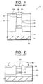
- a conventional optical modulator includes an n-type InP substrate (n-InP substrate) 12, and a layer structure including a 500-nm-thick n-InP lower cladding layer (buffer layer) 14 having a carrier density of 1x10 18 cm -3 , a GaInAsP-based multiple quantum well (MQW) structure or active layer structure 16, a 2000-nm-thick p-InP upper cladding layer 18 having a carrier density of 5x10 17 cm -3 , and a 500-nm-thick p-GaInAs contact layer 20 having a carrier density of 5x10 18 cm -3 , which are consecutively formed on the n-InP substrate 12.
- n-InP substrate n-InP substrate
- buffer layer buffer layer
- MQW multiple quantum well
- the contact layer 20, the p-InP upper cladding layer 18, the MQW structure 16 and the top portion of the n-InP lower cladding layer 14 are configured as a mesa stripe 22, which are abutted and covered by a pair of 2500-nm-thick semi-insulating InP current blocking layers 24 at both sides of the mesa stripe 22.
- the top of the contact layer 20 is exposed from an opening 26 to be in contact with an overlying p-side electrode 30.
- a pair of passivation layers made of SiN cover the InP current blocking layers 24.
- An n-side electrode 32 is formed on the bottom surface of the n-InP substrate 12.
- the conventional optical modulator 10 as described above uses a pair of semi-insulating current blocking layers 24 that abut and cover respective sides of the MQW structure 16. It is considered that this structure is advantageous in the reduction of the parasitic capacitance and improvement for the higher speed operation over another conventional optical modulator having a pair of current blocking layers, each implemented by a p-n junction such as p-InP/n-InP current blocking layers, which abut and cover respective sides of the MQW structure.
- Fig. 2 shows the defective structure we have found around the top electrode 30 in the conventional optical modulator
- Fig. 3 shows an ideal structure for the top electrode 30 of the conventional optical modulator.
- the passivation layer 28 is subjected to patterning for forming the opening 26 to expose the contact layer 20, which is to be connected to the top electrode through the opening 26.
- the margin used for patterning the passivation layer 28 causes the opening 26 to expose the semi-insulating current blocking layers 24 as well as the contact layer 20.
- the p-side electrode 30 made of AuZn for example, is liable to be in contact with the Fe-doped semi-insulating current blocking layers 24, as shown in Fig. 2.
- the top electrode 30 such as shown in Fig. 3, wherein the Fe-doped semi-insulating layers 24 are completely isolated from the top p-side electrode 30.
- This difficulty in fact limited the higher-speed operation of the optical modulator.
- the p-side electrode 30 includes Zn as a constituent element thereof and the Fe-doped current blocking layers include Fe, the Zn content in the p-side electrode 30 and the Fe content in the Fe-doped semi-insulating current blocking layers 24 diffuse mutually across the interface between the p-side electrode 30 and the semi-insulating current blocking layer 24. This mutual diffusion degrades the modulation characteristics of the optical modulator.
- the reduction of the parasitic capacitance around one of the electrodes may be achieved by conventional techniques using a reduced occupied area for the top electrode, and covering the area other than the contact area between the contact layer of the mesa stripe and the top electrode by using a passivation layer.
- these techniques can provide only limited advantages.
- the present invention provides, in one aspect thereof, a semiconductor optical device including: a semiconductor substrate; a layer structure formed as a mesa stripe having sides and overlying the semiconductor substrate; a pair of current blocking layers configured to abut and cover respective sides of the mesa stripe; a pair of Al-oxidized passivation layers formed to cover respective of the pair of current blocking layers, wherein a separation between the Al-oxidized passivation layers defines an opening that exposes a top of the layer structure; a first electrode in contact with the top of the layer structure and extending through the opening; and a second electrode formed on the semiconductor substrate.
- the present invention also provides, in another aspect thereof, a method for manufacturing a semiconductor optical device including the steps of: forming a mesa stripe having sides and a semiconductor layer structure overlying a semiconductor substrate; forming a selective growth mask on the mesa stripe; consecutively growing a pair of current blocking layers and a pair of Al-containing compound semiconductor layers at respective sides of the mesa stripe by using the selective growth mask; selectively oxidizing Al atoms in the Al-containing compound semiconductor layers to form Al-oxidized layers; removing the selective growth mask to form an opening that exposes a top of the mesa stripe; forming a first electrode in contact with the top of the mesa stripe through the opening; and forming a second electrode on the semiconductor substrate.
- the parasitic capacitance involved around the first electrode can be reduced and diffusion of the constituent elements between the first electrode and the current blocking layers can be suppressed.
- the semiconductor optical device has a higher-operational speed and a higher reliability in the device characteristics thereof.
- a semiconductor optical device is implemented as a semiconductor optical modulator of a "buried heterostructure type".
- the optical modulator generally designated by numeral 40, according to the present embodiment includes an n-type InP substrate (n-InP substrate) 12, and a layer structure including a 500-nm-thick n-InP lower cladding layer 14 having a carrier density of 1x10 18 cm -3 , a GaInAsP-based multiple quantum well structure (MQW) or active layer structure 16, a 2000-nm-thick p-InP upper cladding layer 18 having a carrier density of 5x10 17 cm -3 , and a 500-nm-thick p-GaInAs contact layer 20 having a carrier density of 5x10 18 cm -3 , which are consecutively formed on the n-InP substrate 12.
- MQW multiple quantum well structure
- the contact layer 20, the p-InP upper cladding layer 18, the MQW structure 16 and the top portion of the n-InP lower cladding layer 14 are configured as a mesa stripe 22, which are abutted and covered by a pair of 2500-nm-thick semi-insulating InP current blocking layers 24 at respective sides of the mesa stripe 22.
- the top of the contact layer 20 is exposed from an opening 46 to be in contact with an overlying p-side electrode 30.
- a pair of Al-oxidized layer 42 each having a higher electric resistance cover the InP current blocking layers 24.
- the Al-oxidized layer is obtained by selectively oxidizing the Al atoms in an AlInAs layer.
- An n-side electrode 32 is formed on the bottom surface of the n-InP substrate 12.
- the Al-oxidized layers 42 in the embodiment replace the passivation layers made of SiN in the conventional optical modulator.
- the Al-oxidized layer 42 has a specific resistance as high as 10 9 ⁇ -cm.
- the Al-oxidized layer 42 is obtained by selectively oxidizing the Al atoms in an Al-containing compound semiconductor layer, such as AlGaAs layer and AlInAs layer.
- the Al-containing layer such as AlGaAs layer and AlInAs layer, can be grown by a selective growth technique by using a selective growth mask.
- the top p-side electrode 30 which is in electric contact with the contact layer 20 is substantially completely isolated from the semi-insulating current blocking layers 24, thereby reducing the parasitic capacitance involved around the top p-side electrode 30.
- the process for forming the opening in a film by selectively growing the film while using a selective growth mask and removing the selective growth mask may be referred to as a self-alignment process in this text.
- the contact between the top electrode 30 and the Fe-doped current blocking layers 24 does not occur, the mutual diffusion of the Fe content in the current blocking layers 24 and the Zn content in the top electrode 30 can be removed.
- a 500-nm-thick n-InP lower cladding layer 14, a GaInAsP-based MQW structure 16, a 2000-nm-thick p-InP upper cladding layer 18, and a 500-nm-thick p-GaInAs contact layer 20 are consecutively formed on an n-InP substrate 12 as a layer structure.
- a stripe pattern mask 34 made of a dielectric substance such as SiN is formed on the layer structure, followed by etching the contact layer 20, upper cladding layer 18, the MQW structure 16 and a top portion of the lower cladding layer 14 to form a mesa stripe 22.
- a 500-nm-thick semi-insulating InP current blocking layer 24 is selective grown while being doped with Fe to abut and cover respective sides of the mesa stripe 22.
- a 200-nm-thick AlInAs layer 44 is then selectively grown on each of the semi-insulating, Fe-doped InP current blocking layers 24.
- the Al atoms in the AlInAs layer 44 is selectively oxidized at a high temperature in a steam ambient by using a known oxidizing process to form an Al-oxidized layer 42.
- the stripe pattern mask 34 is removed to form an opening 46 between the Al-oxidized layers 24 in a self alignment manner, thereby exposing the contact layer 20.
- a p-side electrode 30 is then formed which is in direct contact with the contact layer 20 through the opening 46.
- An n-side electrode 32 not shown is then formed on the bottom surface of the InP substrate 12, thereby obtaining the structure of Fig. 4.
- the Al-oxidized layer 42 cover the Fe-doped InP current blocking layers 24, thereby preventing the p-side electrode 30 from electrically contacting the Fe-doped InP current blocking layers 24. This improves the isolation between the p-side electrode 30 and the Fe-doped InP current blocking layers 24.
- the opening 46 is formed by removing the selective growth mask 34 in a self-alignment manner, which raises the production yield of the semiconductor optical modulator.
- Samples of the semiconductor optical modulator of the present embodiment were fabricated by the method as described above. The samples were subjected to measurements of the modulation speed, which exhibited an operational speed corresponding to an operational frequency of about 18 GHz.
- a sample of the conventional optical modulator was also fabricated which included a passivation layer made of SiN formed on the InP current blocking layers 24 instead of the Al-oxidized layer 42.
- the sample of the conventional optical modulator had a lower operational speed corresponding to an operational frequency of 15 GHz.
- the sample of the present embodiment exhibited an improvement of 20% in the operational speed.
- the semiconductor optical device and the method for fabricating the semiconductor optical device can be applied to another optical device such as a semiconductor laser device, and integrated optical devices such as a distributed feed-back (DFB) laser device having an EA modulator.
- another optical device such as a semiconductor laser device, and integrated optical devices such as a distributed feed-back (DFB) laser device having an EA modulator.
- DFB distributed feed-back
Landscapes
- Physics & Mathematics (AREA)
- Chemical & Material Sciences (AREA)
- Optics & Photonics (AREA)
- Nonlinear Science (AREA)
- Engineering & Computer Science (AREA)
- Nanotechnology (AREA)
- General Physics & Mathematics (AREA)
- Life Sciences & Earth Sciences (AREA)
- Biophysics (AREA)
- Crystallography & Structural Chemistry (AREA)
- Optical Modulation, Optical Deflection, Nonlinear Optics, Optical Demodulation, Optical Logic Elements (AREA)
- Semiconductor Lasers (AREA)
- Light Receiving Elements (AREA)
Abstract
Description
Claims (4)
- A semiconductor optical device comprising: a semiconductor substrate (12); a layer structure formed as a mesa stripe (22) having sides and overlying said semiconductor substrate (12), a pair of current blocking layers (24) configured to abut and cover respective sides of said mesa stripe; a pair of Al-oxidized passivation layer (42) formed to cover respective of said pair of current blocking layers, wherein a separation between said pair of Al-oxidized passivation layers (42) defines an opening (46) that exposes a top of said layer structure; a first electrode (30) in contact with said top of said layer structure and extending through said opening (46); and a second electrode (32) formed on said semiconductor substrate (12) characterized in that:said Al-oxidized passivation layer (42) is an Al-oxide layer wherein Al atoms in an Al-containing layer is selectively oxidized.
- The semiconductor optical device as defined in claim 1, wherein: each of said current blocking layers (24) is an Fe-doped semi-insulating layer; and said first electrode (30) contains Zn.
- The semiconductor optical device as defined in claim 1, wherein said semiconductor optical device is an optical modulator (40).
- A method for manufacturing a semiconductor optical device comprising the steps of:forming a mesa stripe (22) having sides and a semiconductor layer structure overlying a semiconductor substrate (12);forming a selective growth mask (34) on said mesa stripe (22);consecutively growing a pair of current blocking layers (24) and a pair of an Al-containing compound semiconductor layers (44) at respective sides of said mesa stripe (22) by using said selective growth mask (34);selectively oxidizing Al atoms in said Al-containing compound semiconductor layers (44) to form Al-oxidized layers (44);removing said selective growth mask (34) to form an opening that exposes said mesa stripe (22);forming a first electrode (30) in contact with said mesa stripe (22) through said opening (46); andforming a second electrode (32) on said semiconductor substrate (12).
Applications Claiming Priority (2)
| Application Number | Priority Date | Filing Date | Title |
|---|---|---|---|
| JP2001021708A JP2002228994A (en) | 2001-01-30 | 2001-01-30 | Semiconductor optical device and method of manufacturing the same |
| JP2001021708 | 2001-01-30 |
Publications (2)
| Publication Number | Publication Date |
|---|---|
| EP1227361A2 true EP1227361A2 (en) | 2002-07-31 |
| EP1227361A3 EP1227361A3 (en) | 2004-05-26 |
Family
ID=18887224
Family Applications (1)
| Application Number | Title | Priority Date | Filing Date |
|---|---|---|---|
| EP01120900A Withdrawn EP1227361A3 (en) | 2001-01-30 | 2001-08-30 | Semiconductor optical device having reduced parasitic capacitance |
Country Status (4)
| Country | Link |
|---|---|
| US (1) | US20020100911A1 (en) |
| EP (1) | EP1227361A3 (en) |
| JP (1) | JP2002228994A (en) |
| CA (1) | CA2356176A1 (en) |
Cited By (1)
| Publication number | Priority date | Publication date | Assignee | Title |
|---|---|---|---|---|
| WO2016078057A1 (en) * | 2014-11-20 | 2016-05-26 | 华为技术有限公司 | InP-BASED MODULATOR |
Families Citing this family (2)
| Publication number | Priority date | Publication date | Assignee | Title |
|---|---|---|---|---|
| KR200274179Y1 (en) * | 2002-01-11 | 2002-05-06 | 이광호 | Cushion with vibration motor |
| JP5534826B2 (en) * | 2010-01-19 | 2014-07-02 | 日本オクラロ株式会社 | Semiconductor optical device, optical transmission module, optical transmission / reception module, optical transmission device, and manufacturing method thereof |
Family Cites Families (7)
| Publication number | Priority date | Publication date | Assignee | Title |
|---|---|---|---|---|
| JPS61290790A (en) * | 1985-06-18 | 1986-12-20 | Fujitsu Ltd | Manufacture of light-emitting element |
| JPH05327123A (en) * | 1992-05-20 | 1993-12-10 | Furukawa Electric Co Ltd:The | Semiconductor laser element and its manufacture |
| JPH0918079A (en) * | 1995-06-27 | 1997-01-17 | Mitsubishi Electric Corp | Semiconductor device manufacturing method and semiconductor device |
| JPH0936484A (en) * | 1995-07-14 | 1997-02-07 | Oki Electric Ind Co Ltd | Semiconductor laser and manufacturing method thereof |
| JP3672062B2 (en) * | 1997-07-16 | 2005-07-13 | 三菱電機株式会社 | Semiconductor laser and manufacturing method thereof |
| JP2000216495A (en) * | 1999-01-26 | 2000-08-04 | Nec Corp | Method for manufacturing semiconductor optical device |
| JP2000244049A (en) * | 1999-02-19 | 2000-09-08 | Toshiba Corp | Semiconductor device and manufacturing method thereof |
-
2001
- 2001-01-30 JP JP2001021708A patent/JP2002228994A/en active Pending
- 2001-08-28 CA CA002356176A patent/CA2356176A1/en not_active Abandoned
- 2001-08-29 US US09/940,896 patent/US20020100911A1/en not_active Abandoned
- 2001-08-30 EP EP01120900A patent/EP1227361A3/en not_active Withdrawn
Cited By (1)
| Publication number | Priority date | Publication date | Assignee | Title |
|---|---|---|---|---|
| WO2016078057A1 (en) * | 2014-11-20 | 2016-05-26 | 华为技术有限公司 | InP-BASED MODULATOR |
Also Published As
| Publication number | Publication date |
|---|---|
| EP1227361A3 (en) | 2004-05-26 |
| JP2002228994A (en) | 2002-08-14 |
| CA2356176A1 (en) | 2002-07-30 |
| US20020100911A1 (en) | 2002-08-01 |
Similar Documents
| Publication | Publication Date | Title |
|---|---|---|
| US6798807B2 (en) | Semiconductor laser and semiconductor laser module | |
| US7593445B2 (en) | Semiconductor optical device and optical transmission module | |
| JP3540042B2 (en) | Manufacturing method of semiconductor device | |
| JP3941296B2 (en) | Modulator, semiconductor laser device with modulator, and manufacturing method thereof | |
| JPH07135369A (en) | Semiconductor laser and manufacturing method thereof | |
| US6995454B2 (en) | Semiconductor optical integrated device having a light emitting portion, a modulation section and a separation portion | |
| US6821798B2 (en) | Semiconductor optical device and method for fabricating same | |
| US5804840A (en) | Semiconductor device structure including InAlAs or InAlGaAs current blocking layers | |
| EP0672932B1 (en) | Semiconductor optical modulator | |
| US5179567A (en) | Semiconductor laser device, method of fabricating the same and optical system of utilizing the same | |
| US6931041B2 (en) | Integrated semiconductor laser device and method of manufacture thereof | |
| US6200826B1 (en) | Method of fabricating a reverse mesa ridge waveguide type laser diode | |
| US7288422B2 (en) | Photonic integrated device using reverse-mesa structure and method for fabricating the same | |
| US20020100911A1 (en) | Semiconductor optical device having reduced parasitic capacitance | |
| JP2002232080A (en) | Semiconductor device having current confinement structure and method of manufacturing the same | |
| JPH03263388A (en) | Optical semiconductor element and manufacture thereof | |
| US6031857A (en) | Semiconductor device having a current-constricting spaces and method of manufacturing the device | |
| KR100584332B1 (en) | Laser device with integrated field absorption modulator and manufacturing method thereof | |
| US6937632B2 (en) | Integrated semiconductor laser and waveguide device | |
| JP4164248B2 (en) | Semiconductor element, manufacturing method thereof, and semiconductor optical device | |
| JPH11121787A (en) | Integrated optical device and method of manufacturing the same | |
| US20250138347A1 (en) | Semiconductor optical integrated device | |
| US20220254940A1 (en) | Light-receiving device and method of manufacturing light-receiving device | |
| JPS63211788A (en) | Semiconductor laser and manufacture thereof | |
| JPH1124020A (en) | Embedded semiconductor optical function device |
Legal Events
| Date | Code | Title | Description |
|---|---|---|---|
| PUAI | Public reference made under article 153(3) epc to a published international application that has entered the european phase |
Free format text: ORIGINAL CODE: 0009012 |
|
| AK | Designated contracting states |
Kind code of ref document: A2 Designated state(s): AT BE CH CY DE DK ES FI FR GB GR IE IT LI LU MC NL PT SE TR |
|
| AX | Request for extension of the european patent |
Free format text: AL;LT;LV;MK;RO;SI |
|
| PUAL | Search report despatched |
Free format text: ORIGINAL CODE: 0009013 |
|
| AK | Designated contracting states |
Kind code of ref document: A3 Designated state(s): AT BE CH CY DE DK ES FI FR GB GR IE IT LI LU MC NL PT SE TR |
|
| AX | Request for extension of the european patent |
Extension state: AL LT LV MK RO SI |
|
| RIC1 | Information provided on ipc code assigned before grant |
Ipc: 7H 01S 5/026 B Ipc: 7G 02F 1/025 B Ipc: 7G 02F 1/1362 A |
|
| AKX | Designation fees paid | ||
| REG | Reference to a national code |
Ref country code: DE Ref legal event code: 8566 |
|
| STAA | Information on the status of an ep patent application or granted ep patent |
Free format text: STATUS: THE APPLICATION IS DEEMED TO BE WITHDRAWN |
|
| 18D | Application deemed to be withdrawn |
Effective date: 20041127 |