EP1227345A2 - Diffractive optical element - Google Patents
Diffractive optical element Download PDFInfo
- Publication number
- EP1227345A2 EP1227345A2 EP02001699A EP02001699A EP1227345A2 EP 1227345 A2 EP1227345 A2 EP 1227345A2 EP 02001699 A EP02001699 A EP 02001699A EP 02001699 A EP02001699 A EP 02001699A EP 1227345 A2 EP1227345 A2 EP 1227345A2
- Authority
- EP
- European Patent Office
- Prior art keywords
- substrate
- optical element
- film layer
- diffractive optical
- upper film
- Prior art date
- Legal status (The legal status is an assumption and is not a legal conclusion. Google has not performed a legal analysis and makes no representation as to the accuracy of the status listed.)
- Granted
Links
Images


Classifications
-
- G—PHYSICS
- G02—OPTICS
- G02B—OPTICAL ELEMENTS, SYSTEMS OR APPARATUS
- G02B5/00—Optical elements other than lenses
- G02B5/18—Diffraction gratings
- G02B5/1847—Manufacturing methods
- G02B5/1857—Manufacturing methods using exposure or etching means, e.g. holography, photolithography, exposure to electron or ion beams
Definitions
- the present invention relates to an improved diffraction optical element (DOE).
- DOE diffraction optical element
- the DOE having a smoothly etched surface substrate.
- the DOE utilizes optical diffraction and directly controls the optical phases, and therefore, a wide range of applications including, multi-spot beam splitters, for example, can be expected.
- the DOE can split one processing laser beam into multiple spots. Simultaneous processing at plural spots, shaping patterns such as marking, and non-circular-shape processing have been achieved with highspeed.
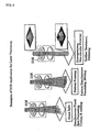
- Figure 4 shows an example wherein the DOE is utilized in drill processing using a carbon dioxide gas laser to split one processing laser beam into multiple spots and simultaneously drill a plurality of holes.
- the present invention provides an improved DOE which has a smoothly etched surface.
- the DOE of the present invention comprises a polycrystalline substrate which has an upper film layer having the same material as the substrate, and having finer polycrystalline grains than that of the substrate or having an amorphous phase laminated on the substrate.
- the DOE be provided with a polycrystalline substrate whose diameter of crystal grains at an etched surface is not more than1 ⁇ m.
- the DOE be provided with an amorphous phase at an etched surface of the substrate.
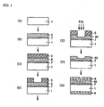
- Figure 1 is a diagram showing the general steps for manufacturing the DOE related to the preferred embodiment of the present invention.
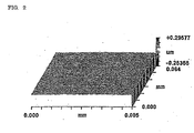
- Figure 2 shows a surface state of zinc selenide (ZnSe) vapor-deposited film after dry etching according to the present invention.
- Figure 3 shows a process flow chart of manufacturing a conventional DOE.
- Figure 4 shows an example of the DOE application to the laser drill processing.
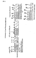
- Figure 5 shows three examples of the DOE application to other laser processing.
- Figure 6 is a schematic figure showing problems during manufacturing conventional DOE with the use of hydrocarbon gas.
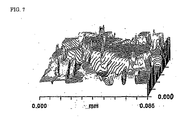
- Figure 7 shows the surface state of a ZnSe substrate after conventional direct etching.
- ZnSe having excellent transmittance at infrared optical wavelength, has been used as material of optical elements for a carbon dioxide gas laser (utilizing wavelength is 9.3 ⁇ m or 10.6 ⁇ m).
- a carbon dioxide gas laser utilizing wavelength is 9.3 ⁇ m or 10.6 ⁇ m.
- polycrystals have been used instead of a single crystal considering the cost aspect.
- CVD chemical vapor deposition
- RIE reactive ion etching
- Hydrocarbon-based gas which is commonly used for a single crystal, has been known as etching gas of the RIE method.
- etching gas of the RIE method Hydrocarbon-based gas
- the etching rate depends heavily on the crystal orientation of the polycrystalline grains.
- the surface of the ZnSe polycrystals becomes rough, deteriorating the optical characteristics of the DOE such as deviation of the diffracted optical intensity and focussed position accuracy.
- the present invention provides an improved DOE which has a smoothly etched surface.
- the DOE of the present invention comprises a polycrystalline substrate which has an upper film layer having the same material as the substrate, and having finer polycrystalline grains than that of the substrate or having an amorphous phase laminated on the substrate.
- the surface having finer polycrystalline grains or an amorphous phase can be easily obtained by laminating an upper film layer.
- the DOE of the present invention is preferably provided with a polycrystalline substrate whose sizes of crystal grains at an etched surface are not more than about 1 ⁇ m.
- the sizes of crystal grains at an etched surface are more desirably not more than about 0.5 ⁇ m, because smaller diameter of crystal grains improves the precision of the etched surface.
- the DOE of the present invention is also preferably provided with an amorphous phase substrate at an etched surface.
- the reason is that a more smoothly etched surface can be obtained because of the surface having no crystal grain.
- the surface having finer crystal grains or an amorphous phase can be obtained by selecting an appropriate laminating condition, or applying heat treatments, surface treatments and so on.
- the etching rate of the surface becomes more even than that of conventional polycrystalline substrates. This is because the finer polycrystalline layer or the amorphous phase layer is less affected by the etching rate dependency on the crystal orientation, compared with the conventional substrate having coarse polycrystalline grains. As a result, the surface of the DOE of the present invention is improved to become smooth and then the deviation of the optical diffraction intensity and/or optical irradiated position becomes small.
- a buffer layer between the upper film layer and the substrate is more suitably provided in order to prevent peeling-off of the upper film layer from the substrate.
- the buffer layer is preferably selected from materials suitable for transmitting a light at operating wavelength.
- Materials for the buffer layer are preferably to have an optical absorption coefficient not more than 10 cm -1 . Considering the buffer layer thickness to prevent peeling-off, an optical absorption coefficient is limited to the above-described value.
- ZnSe is more suitable for the polycrystalline substrate, especially for a carbon-dioxide-laser-DOE in the present invention.
- the substrate is formed by the CVD method, because a high purity substrate which is superior in the optical transmittance can be obtained.
- the buffer layer is preferably selected from one of the fluorine compounds such as barium di-fluoride (BaF 2 ), thorium tetra-fluoride (ThF 4 ) and ytterbium tri-fluoride (YbF 3 ) for the carbon-dioxide-laser-DOE.
- the fluorine compounds such as barium di-fluoride (BaF 2 ), thorium tetra-fluoride (ThF 4 ) and ytterbium tri-fluoride (YbF 3 ) for the carbon-dioxide-laser-DOE.
- the buffer layer be formed by a vapor phase growing method, because a high purity layer which is superior to the optical transmittance can be obtained for the same reason as in the substrate.
- the upper film layer and the buffer layer may be formed by one of the vapor deposition method (Electron Beam method, Ion Assist method, and Resistant Heat method). This is because the thickness of the film layer can be easily controlled by such methods.
- the etching method is preferably applied by a dry etching method, and more suitably a RIE method.
- the precision of an etched shape improves, because the etching direction has greater controllability compared with the plasma etching method
- Figure 1 is an example of a schematic sectional view in each step of manufacturing a semiconductor device for a DOE according to the present invention.
- Step A A ZnSe polycrystalline substrate 1 is prepared.
- Step B A ThF 4 film 7 is formed on the substrate 1.
- An upper film layer having the same material as the substrate and having finer polycrystalline grains than those of the substrate or an amorphous phase is laminated on the film 7.
- a ZnSe film layer 8 is laminated as the upper film layer.
- the thickness of at least 3 ⁇ m is necessary for the ZnSe upper film layer 8, because the etching depth of at least 3 ⁇ m is necessary in the upper film layer.
- the ThF 4 film layer 7 is to prevent peeling-off of the ZnSe upper film layer 8 from the polycrystalline substrate 1.
- the ThF 4 film layer 7 is unnecessary under the condition that the detachment of the ZnSe upper film layer 8 from the polycrystalline substrate 1 can be prevented.
- the ZnSe upper film layer 8 can be improved adhesion properties by applying a surface treatment in the dry or wet process in order to remove a surface layer which is changed quality during a surface polishing or contained impurities thereof. By applying the above treatment, such ThF 4 film layer 7 can be omitted.
- Step C A resist layer 2 is formed on the ZnSe upper film layer 8.
- Step D The resist layer 2 is selectively irradiated by means of a photomask (not shown) and formed a printed pattern thereon. Then, by developing the resist layer 2, a resist pattern 5 is formed.
- Step E The ZnSe upper film layer 8 is dry etched with RIE method by using the resist pattern 5 as a mask to form a patterned ZnSe upper film layer 80.
- the etching rate is not strongly affected by the crystal orientation.
- a surface layer having fine crystal grains or an amorphous phase has random crystal-oriented grains or no crystal grain, etching rate of the substrate is not dependent on the crystal orientation as a whole. That is the reason why the etched surface of the ZnSe upper film layer 80 does not become coarse.
- Step F The resist pattern 5 is removed.
- Step G After anti-reflection (AR) coating 6 has been formed on the ZnSe upper film layer 80 and a bottom surface of the polycrystalline substrate 1, DOE manufacturing is completed.
- AR anti-reflection
- a polycrystalline ZnSe with crystal grain sizes of about 60 ⁇ m, manufactured by the CVD method had been cut and polished to form a substrate having a diameter of 50 mm and a thickness of 5 mm (whose surface roughness (Ra) was 2 nm).
- a ThF 4 film layer of 0.2 ⁇ m thickness and a ZnSe upper film layer having a thickness of 6 ⁇ m were laminated on the polished substrate by the resistance-heat vapor deposition method.
- the ZnSe upper film layer had crystalline having crystal grains of about 0.06 ⁇ m width in a growth direction.
- the Ra of the ZnSe upper film layer was 2 nm, which is the same as the ZnSe substrate.
- the ZnSe upper film layer deposited on the ZnSe substrate was etched by the RIE method.
- the etching condition was as follows:
- Figure 2 shows a surface state of the etched ZnSe upper film layer in the present invention. It was confirmed that the surface was not rough. Etching depth was about 4 ⁇ m, and Ra was 3 nm.
- the DOE obtained by the example showed satisfactory optical characteristics for DOE.
- a DOE using polycrystalline ZnSe was manufactured by the following steps as shown in Fig. 3.
- Step A A polycrystalline ZnSe was synthesized from Zn and H 2 Se by the chemical reaction: Zn + H 2 Se ⁇ ZnSe + H 2 .
- Step B The polycrystalline ZnSe was cut and a ZnSe polycrystalline substrate 1 was formed, and the surface thereof was polished.
- Step C A resist layer 2 was formed on the ZnSe polycrystalline substrate 1.
- Step D Light 4 was selectively irradiated on the resist layer 2 by means of a photomask 3 to form a printed pattern thereon.
- Step E The resist layer 2 was developed to form a resist pattern 5.
- Step F RIE with the use of hydrocarbon gas, which had been normally used in single crystal processing, was performed on the ZnSe polycrystalline substrate 1 using the resist pattern 5 to form a patterned ZnSe polycrystalline substrate 10.
- Step G The resist pattern 5 was removed to form the patterned ZnSe polycrystalline substrate 10.
- Step H An anti-deflection (AR) coating layer 6 was formed on both surfaces of the patterned ZnSe polycrystalline substrate 10.
- Figure 7 shows a surface of the ZnSe substrate which has no vapor deposited film layer on the ZnSe polycrystalline substrate and directly etched on the same condition as mentioned above.
- the etching depth was about 4 ⁇ m, and the Ra was 80 nm.
- the surface state was not a mirror surface.
- the DOE obtained by the comparative example showed inferior optical characteristics compared with that obtained by the example.
Landscapes
- Physics & Mathematics (AREA)
- Engineering & Computer Science (AREA)
- Manufacturing & Machinery (AREA)
- General Physics & Mathematics (AREA)
- Optics & Photonics (AREA)
- Diffracting Gratings Or Hologram Optical Elements (AREA)
- Drying Of Semiconductors (AREA)
- Surface Treatment Of Optical Elements (AREA)
- Micromachines (AREA)
Abstract
Description
Claims (10)
- A diffractive optical element comprisinga polycrystalline substrate andan upper film layer which is laminated on the substrate, wherein the material of the upper film layer
is the same material as the substrate, and having finer crystal grains compared with crystal grains of
the substrate or having an amorphous phase, andthe upper film layer is dry etched. - A diffractive optical element according to claim 1, further comprising a buffer layer provided between the substrate and the upper film layer.
- A diffractive optical element according to claim 2, wherein the buffer layer is selected from the materials having an optical absorption coefficient of not more than 10 cm-1 at operating wavelength.
- A diffractive optical element according to any one of claims 1 to 3, wherein the substrate is made of ZnSe.
- A diffractive optical element according to claim 4, wherein the substrate is formed by a chemical vapor deposition method.
- A diffractive optical element according to claim 2, wherein the buffer layer is made of a fluorine compound.
- A diffractive optical element according to claim 2, wherein the upper film layer and the buffer layer are formed by a vapor phase growth method.
- A diffractive optical element according to claim 2, wherein the upper film layer and the buffer layer are formed by a vapor deposition method.
- A diffractive optical element according to claim 1, wherein the dry etching is performed by a reactive ion etching method.
- A diffractive optical element for carbon dioxide gas laser comprising a substrate having polycrystals whose crystal grain size is not more than about 1 µm, or having an amorphous phase at the dry-etched surface thereof.
Applications Claiming Priority (2)
| Application Number | Priority Date | Filing Date | Title |
|---|---|---|---|
| JP2001019432A JP3501127B2 (en) | 2001-01-29 | 2001-01-29 | Diffractive optical components |
| JP2001019432 | 2001-01-29 |
Publications (3)
| Publication Number | Publication Date |
|---|---|
| EP1227345A2 true EP1227345A2 (en) | 2002-07-31 |
| EP1227345A3 EP1227345A3 (en) | 2002-10-02 |
| EP1227345B1 EP1227345B1 (en) | 2004-03-31 |
Family
ID=18885308
Family Applications (1)
| Application Number | Title | Priority Date | Filing Date |
|---|---|---|---|
| EP02001699A Expired - Lifetime EP1227345B1 (en) | 2001-01-29 | 2002-01-24 | Diffractive optical element |
Country Status (5)
| Country | Link |
|---|---|
| US (1) | US6775066B2 (en) |
| EP (1) | EP1227345B1 (en) |
| JP (1) | JP3501127B2 (en) |
| CA (1) | CA2369063C (en) |
| DE (1) | DE60200300T2 (en) |
Families Citing this family (9)
| Publication number | Priority date | Publication date | Assignee | Title |
|---|---|---|---|---|
| US7327760B1 (en) | 2001-05-08 | 2008-02-05 | Cortina Systems, Inc. | Multi-service segmentation and reassembly device operable with either a cell-based or a packet-based switch fabric |
| US7256938B2 (en) * | 2004-03-17 | 2007-08-14 | General Atomics | Method for making large scale multilayer dielectric diffraction gratings on thick substrates using reactive ion etching |
| US7528073B2 (en) | 2004-11-04 | 2009-05-05 | Sumitomo Electric Industries, Ltd. | Dry etching method and diffractive optical element |
| US7321467B2 (en) * | 2005-05-26 | 2008-01-22 | Macronix International Co., Ltd. | Anti-reflection coating layer and design method thereof |
| US7821900B2 (en) * | 2008-05-15 | 2010-10-26 | Northrop Grumman Systems Corporation | Diffractive optical element and method of designing the same |
| JP5249064B2 (en) | 2009-01-19 | 2013-07-31 | 住友電気工業株式会社 | Method for manufacturing diffractive optical component |
| JP5424154B2 (en) | 2010-04-28 | 2014-02-26 | 公立大学法人大阪府立大学 | Optical components |
| JP2013186350A (en) | 2012-03-08 | 2013-09-19 | Canon Inc | Calculation method for structure data of diffraction optical element, program, and manufacturing method |
| CN109520621B (en) * | 2017-09-19 | 2026-05-15 | 睿励科学仪器(上海)有限公司 | Three-dimensional spatial light source system and related optical measurement equipment |
Family Cites Families (4)
| Publication number | Priority date | Publication date | Assignee | Title |
|---|---|---|---|---|
| DE4338969C2 (en) | 1993-06-18 | 1996-09-19 | Schott Glaswerke | Process for the production of inorganic diffractive elements and use thereof |
| JPH10300912A (en) | 1997-04-30 | 1998-11-13 | Shimadzu Corp | Substrate for diffraction grating |
| JP2000280225A (en) | 1999-04-02 | 2000-10-10 | Murata Mfg Co Ltd | Processing method and processing apparatus for ceramic green sheet |
| JP4148382B2 (en) | 1999-04-02 | 2008-09-10 | 株式会社村田製作所 | Processing method of ceramic green sheet |
-
2001
- 2001-01-29 JP JP2001019432A patent/JP3501127B2/en not_active Expired - Fee Related
-
2002
- 2002-01-22 US US10/051,023 patent/US6775066B2/en not_active Expired - Lifetime
- 2002-01-23 CA CA002369063A patent/CA2369063C/en not_active Expired - Fee Related
- 2002-01-24 DE DE60200300T patent/DE60200300T2/en not_active Expired - Lifetime
- 2002-01-24 EP EP02001699A patent/EP1227345B1/en not_active Expired - Lifetime
Also Published As
| Publication number | Publication date |
|---|---|
| DE60200300D1 (en) | 2004-05-06 |
| US20020101663A1 (en) | 2002-08-01 |
| EP1227345A3 (en) | 2002-10-02 |
| JP2002221614A (en) | 2002-08-09 |
| DE60200300T2 (en) | 2004-08-05 |
| CA2369063C (en) | 2005-04-05 |
| CA2369063A1 (en) | 2002-07-29 |
| US6775066B2 (en) | 2004-08-10 |
| EP1227345B1 (en) | 2004-03-31 |
| JP3501127B2 (en) | 2004-03-02 |
Similar Documents
| Publication | Publication Date | Title |
|---|---|---|
| US7115341B2 (en) | Halftone phase shift mask blank, halftone phase shift mask, and method of producing the same | |
| US5674356A (en) | Method for forming a semiconductor device in which an anti reflective layer is formed by varying the composition thereof | |
| JP5356516B2 (en) | Concave and convex pattern forming method | |
| EP3167476B1 (en) | Extreme ultraviolet reflective element with amorphous layers and method of manufacturing thereof | |
| US7415096B2 (en) | Curved X-ray reflector | |
| US7294438B2 (en) | Method of producing a reflective mask and method of producing a semiconductor device | |
| US20110206859A1 (en) | Engineered fluoride-coated elements for laser systems | |
| EP1227345B1 (en) | Diffractive optical element | |
| US20030162005A1 (en) | Reflective-type mask blank for exposure, method of producing the same, and reflective-type mask for exposure | |
| EP0788027B1 (en) | Phase shift mask blank and production method therefor | |
| US20090280415A1 (en) | Transparent substrate for mask blank and mask blank | |
| JP3818171B2 (en) | Phase shift mask blank and manufacturing method thereof | |
| US7842606B2 (en) | Method of depositing thin film and method of manufacturing semiconductor using the same | |
| JP2003249434A (en) | Exposure reflective mask blank and exposure reflective mask | |
| CN118742845A (en) | Ferroelectric device or structure and method for producing a ferroelectric device or structure | |
| US6603601B2 (en) | Infrared laser optical element and manufacturing method therefor | |
| US6998204B2 (en) | Alternating phase mask built by additive film deposition | |
| CN117631110A (en) | A buried reflective all-dielectric diffraction grating and its preparation method | |
| JP3473580B2 (en) | Method for manufacturing diffractive optical component of ZnSe polycrystal for carbon dioxide laser | |
| JP2000003029A (en) | Photomask and method of manufacturing photomask | |
| JPH10300912A (en) | Substrate for diffraction grating | |
| JP4073882B2 (en) | Halftone phase shift mask blank | |
| JP2025146050A (en) | Reflective mask blank, reflective mask, and method for manufacturing a reflective mask | |
| WO2025192373A1 (en) | Reflective mask blank, reflective mask, and method for manufacturing reflective mask | |
| EP1502970A1 (en) | Znse diffraction type optical component and method for fabricating the same |
Legal Events
| Date | Code | Title | Description |
|---|---|---|---|
| PUAI | Public reference made under article 153(3) epc to a published international application that has entered the european phase |
Free format text: ORIGINAL CODE: 0009012 |
|
| AK | Designated contracting states |
Kind code of ref document: A2 Designated state(s): AT BE CH CY DE DK ES FI FR GB GR IE IT LI LU MC NL PT SE TR |
|
| AX | Request for extension of the european patent |
Free format text: AL;LT;LV;MK;RO;SI |
|
| PUAL | Search report despatched |
Free format text: ORIGINAL CODE: 0009013 |
|
| AK | Designated contracting states |
Kind code of ref document: A3 Designated state(s): AT BE CH CY DE DK ES FI FR GB GR IE IT LI LU MC NL PT SE TR |
|
| AX | Request for extension of the european patent |
Free format text: AL;LT;LV;MK;RO;SI |
|
| 17P | Request for examination filed |
Effective date: 20020924 |
|
| GRAH | Despatch of communication of intention to grant a patent |
Free format text: ORIGINAL CODE: EPIDOS IGRA |
|
| RIN1 | Information on inventor provided before grant (corrected) |
Inventor name: FUSE, KEIJI,OSAKA WORKS OF SUMITOMO Inventor name: KURISU, KENICHI,OSAKA WORKS OF SUMITOMO |
|
| AKX | Designation fees paid |
Designated state(s): DE GB |
|
| GRAS | Grant fee paid |
Free format text: ORIGINAL CODE: EPIDOSNIGR3 |
|
| GRAA | (expected) grant |
Free format text: ORIGINAL CODE: 0009210 |
|
| AK | Designated contracting states |
Kind code of ref document: B1 Designated state(s): DE GB |
|
| REG | Reference to a national code |
Ref country code: GB Ref legal event code: FG4D |
|
| REG | Reference to a national code |
Ref country code: IE Ref legal event code: FG4D |
|
| REF | Corresponds to: |
Ref document number: 60200300 Country of ref document: DE Date of ref document: 20040506 Kind code of ref document: P |
|
| PLBE | No opposition filed within time limit |
Free format text: ORIGINAL CODE: 0009261 |
|
| STAA | Information on the status of an ep patent application or granted ep patent |
Free format text: STATUS: NO OPPOSITION FILED WITHIN TIME LIMIT |
|
| 26N | No opposition filed |
Effective date: 20050104 |
|
| PGFP | Annual fee paid to national office [announced via postgrant information from national office to epo] |
Ref country code: GB Payment date: 20190123 Year of fee payment: 18 |
|
| PGFP | Annual fee paid to national office [announced via postgrant information from national office to epo] |
Ref country code: DE Payment date: 20200114 Year of fee payment: 19 |
|
| GBPC | Gb: european patent ceased through non-payment of renewal fee |
Effective date: 20200124 |
|
| PG25 | Lapsed in a contracting state [announced via postgrant information from national office to epo] |
Ref country code: GB Free format text: LAPSE BECAUSE OF NON-PAYMENT OF DUE FEES Effective date: 20200124 |
|
| REG | Reference to a national code |
Ref country code: DE Ref legal event code: R119 Ref document number: 60200300 Country of ref document: DE |
|
| PG25 | Lapsed in a contracting state [announced via postgrant information from national office to epo] |
Ref country code: DE Free format text: LAPSE BECAUSE OF NON-PAYMENT OF DUE FEES Effective date: 20210803 |