EP1226951A2 - Power-saving thermal head - Google Patents
Power-saving thermal head Download PDFInfo
- Publication number
- EP1226951A2 EP1226951A2 EP02250258A EP02250258A EP1226951A2 EP 1226951 A2 EP1226951 A2 EP 1226951A2 EP 02250258 A EP02250258 A EP 02250258A EP 02250258 A EP02250258 A EP 02250258A EP 1226951 A2 EP1226951 A2 EP 1226951A2
- Authority
- EP
- European Patent Office
- Prior art keywords
- insulation layer
- thermal insulation
- heating resistor
- thermal
- resistor elements
- Prior art date
- Legal status (The legal status is an assumption and is not a legal conclusion. Google has not performed a legal analysis and makes no representation as to the accuracy of the status listed.)
- Withdrawn
Links
Images



Classifications
-
- B—PERFORMING OPERATIONS; TRANSPORTING
- B41—PRINTING; LINING MACHINES; TYPEWRITERS; STAMPS
- B41J—TYPEWRITERS; SELECTIVE PRINTING MECHANISMS, i.e. MECHANISMS PRINTING OTHERWISE THAN FROM A FORME; CORRECTION OF TYPOGRAPHICAL ERRORS
- B41J2/00—Typewriters or selective printing mechanisms characterised by the printing or marking process for which they are designed
- B41J2/315—Typewriters or selective printing mechanisms characterised by the printing or marking process for which they are designed characterised by selective application of heat to a heat sensitive printing or impression-transfer material
- B41J2/32—Typewriters or selective printing mechanisms characterised by the printing or marking process for which they are designed characterised by selective application of heat to a heat sensitive printing or impression-transfer material using thermal heads
- B41J2/335—Structure of thermal heads
- B41J2/33505—Constructional details
- B41J2/33525—Passivation layers
-
- B—PERFORMING OPERATIONS; TRANSPORTING
- B41—PRINTING; LINING MACHINES; TYPEWRITERS; STAMPS
- B41J—TYPEWRITERS; SELECTIVE PRINTING MECHANISMS, i.e. MECHANISMS PRINTING OTHERWISE THAN FROM A FORME; CORRECTION OF TYPOGRAPHICAL ERRORS
- B41J2/00—Typewriters or selective printing mechanisms characterised by the printing or marking process for which they are designed
- B41J2/315—Typewriters or selective printing mechanisms characterised by the printing or marking process for which they are designed characterised by selective application of heat to a heat sensitive printing or impression-transfer material
- B41J2/32—Typewriters or selective printing mechanisms characterised by the printing or marking process for which they are designed characterised by selective application of heat to a heat sensitive printing or impression-transfer material using thermal heads
- B41J2/335—Structure of thermal heads
- B41J2/33505—Constructional details
- B41J2/3353—Protective layers
-
- B—PERFORMING OPERATIONS; TRANSPORTING
- B41—PRINTING; LINING MACHINES; TYPEWRITERS; STAMPS
- B41J—TYPEWRITERS; SELECTIVE PRINTING MECHANISMS, i.e. MECHANISMS PRINTING OTHERWISE THAN FROM A FORME; CORRECTION OF TYPOGRAPHICAL ERRORS
- B41J2/00—Typewriters or selective printing mechanisms characterised by the printing or marking process for which they are designed
- B41J2/315—Typewriters or selective printing mechanisms characterised by the printing or marking process for which they are designed characterised by selective application of heat to a heat sensitive printing or impression-transfer material
- B41J2/32—Typewriters or selective printing mechanisms characterised by the printing or marking process for which they are designed characterised by selective application of heat to a heat sensitive printing or impression-transfer material using thermal heads
- B41J2/335—Structure of thermal heads
- B41J2/33545—Structure of thermal heads characterised by dimensions
-
- B—PERFORMING OPERATIONS; TRANSPORTING
- B41—PRINTING; LINING MACHINES; TYPEWRITERS; STAMPS
- B41J—TYPEWRITERS; SELECTIVE PRINTING MECHANISMS, i.e. MECHANISMS PRINTING OTHERWISE THAN FROM A FORME; CORRECTION OF TYPOGRAPHICAL ERRORS
- B41J2/00—Typewriters or selective printing mechanisms characterised by the printing or marking process for which they are designed
- B41J2/315—Typewriters or selective printing mechanisms characterised by the printing or marking process for which they are designed characterised by selective application of heat to a heat sensitive printing or impression-transfer material
- B41J2/32—Typewriters or selective printing mechanisms characterised by the printing or marking process for which they are designed characterised by selective application of heat to a heat sensitive printing or impression-transfer material using thermal heads
- B41J2/335—Structure of thermal heads
- B41J2/3355—Structure of thermal heads characterised by materials
-
- B—PERFORMING OPERATIONS; TRANSPORTING
- B41—PRINTING; LINING MACHINES; TYPEWRITERS; STAMPS
- B41J—TYPEWRITERS; SELECTIVE PRINTING MECHANISMS, i.e. MECHANISMS PRINTING OTHERWISE THAN FROM A FORME; CORRECTION OF TYPOGRAPHICAL ERRORS
- B41J2/00—Typewriters or selective printing mechanisms characterised by the printing or marking process for which they are designed
- B41J2/315—Typewriters or selective printing mechanisms characterised by the printing or marking process for which they are designed characterised by selective application of heat to a heat sensitive printing or impression-transfer material
- B41J2/32—Typewriters or selective printing mechanisms characterised by the printing or marking process for which they are designed characterised by selective application of heat to a heat sensitive printing or impression-transfer material using thermal heads
- B41J2/335—Structure of thermal heads
- B41J2/33555—Structure of thermal heads characterised by type
- B41J2/3357—Surface type resistors
-
- B—PERFORMING OPERATIONS; TRANSPORTING
- B41—PRINTING; LINING MACHINES; TYPEWRITERS; STAMPS
- B41J—TYPEWRITERS; SELECTIVE PRINTING MECHANISMS, i.e. MECHANISMS PRINTING OTHERWISE THAN FROM A FORME; CORRECTION OF TYPOGRAPHICAL ERRORS
- B41J2/00—Typewriters or selective printing mechanisms characterised by the printing or marking process for which they are designed
- B41J2/315—Typewriters or selective printing mechanisms characterised by the printing or marking process for which they are designed characterised by selective application of heat to a heat sensitive printing or impression-transfer material
- B41J2/32—Typewriters or selective printing mechanisms characterised by the printing or marking process for which they are designed characterised by selective application of heat to a heat sensitive printing or impression-transfer material using thermal heads
- B41J2/335—Structure of thermal heads
- B41J2/3358—Cooling arrangements
Definitions
- This invention relates to a high efficiency thermal head to be used for a thermal printer and a method for manufacture of the thermal head.
- a conventional thermal head is provided with a glaze thermal insulation layer 102 formed of alumina having a thickness of approximately 80 ⁇ m formed on the top face of a radiative substrate 101 and a convex 102a having a height of approximately 5 ⁇ m formed by means of the photolithographic technique on the top face of the glaze insulation layer 102.
- a heating resistor 103 formed of Ta-SiO 2 is formed on the top face of the glaze thermal insulation layer 102 by means of the sputtering technique and photolithographic technique so as to form a pattern. Furthermore, a part of the heating resistor 103 functions as a heating element 103a arranged at an equal intervals on the space between a common electrode 104a and an individual electrode 104b, which will be described hereinafter.
- a heating resistor that has been subjected to high temperature stabilization heat treatment at 500 to 800 °C after film forming is used as the heating resistor 103.
- the high temperature stabilization heat treatment of the heating resistor 103 brings about the improved characteristic of the heating resistor 103 so that heating in printing does not result in increased resistance loss, and so that a heating head prints without irregular printing density.
- a power supplier 104 that functions to supply electric energy to the heating resistor 103 having a thickness of approximately 2 ⁇ m consisting of a metal material such as Al, Cu, or Au is formed by means of sputtering, and the common electrode 104a, the individual electrode 104b, and outside-connection terminals (not shown in the drawing) of the electrodes 104a and 104b are formed by means of the photolithographic technique.
- a protection layer 105 that functions to prevent wearing and oxidation of the heating resistor 103 and the electrodes 104a and 104b is formed.
- the protection layer 105 is formed of a layer having a thickness of approximately 5 to 10 ⁇ m consisting of hard ceramic such as Si-O-N or Si-Al-O-N formed by means of sputtering.
- a current is supplied selectively to the common electrode 104a and individual electrode 104b to heat the heating element 103a so as to transfer ink of an ink ribbon onto plain paper and so as to print a desired character or a desired image. Otherwise, a desired character or a desired image is printed directly on heat sensitive paper.
- a thermal printer having a conventional thermal head as described hereinabove that is portable and driven by use of a battery has been available commercially.
- the thermal head of the portable printer as described hereinabove is the biggest power consumer, and it particularly causes the short life of a battery.
- a power-saving thermal head has been expected to be developed.
- the film thickness of the glaze should be thick.
- forming of a glaze thermal insulation layer 102 having a thickness thicker than current 80 ⁇ m is difficult technically and the thickness is limited on the film forming technique reason. As the result, no power-saving thermal head has been developed.
- the high temperature stabilization heat treatment at a temperature of 500 to 800 °C is required to obtain a conventional thermal head after a heating resistor 103 is molded, and the thermal treatment results in a complex manufacturing process and the thermal treatment requires calcination equipment, which results in the high cost.
- the present invention has been accomplished in view of the abovementioned problem, and provides a thermal head and a method for manufacture of the same that is capable of saving power and bringing about the low cost.
- the first means is characterized in that a thermal head is provided with a thermal insulation layer formed on a radiative substrate, a plurality of heating resistor elements formed on a top face of the thermal insulation layer, a power supplier comprising an individual electrode and a common electrode connected to the heating resistor elements to supply power to the heating resistor, and a protection layer that covers surfaces of at least the heating resistor elements and the power supplier, wherein the thermal insulation layer is formed by laminating an inorganic thermal insulation layer consisting of ceramic mainly containing Si, transition metal, and oxygen and/or nitrogen on an organic thermal insulation layer consisting of polyimide resin.
- the second means is characterized in that a thermal head is provided with a thermal insulation layer formed on a radiative substrate, a plurality of heating resistor elements formed on a top face of the thermal insulation layer, a power supplier comprising an individual electrode and a common electrode connected to the heating resistor elements to supply power to the heating resistor, and a protection layer that covers surfaces of at least the heating resistor elements and the power supplier, wherein the thermal insulation layer is formed by laminating an inorganic thermal insulation layer consisting of ceramic mainly containing Si, transition metal, and oxygen and/or nitrogen on an organic thermal insulation layer consisting of polyimide resin, an inorganic protection layer consisting of oxide of Si or Al, or nitride, or carbide is additionally formed on a top face of the inorganic thermal insulation layer, and the heating elements are formed on a top face of the inorganic protection layer.
- the third means is characterized in that a thermal head is provided with a thermal insulation layer formed on a radiative substrate, a plurality of heating resistor elements formed on a top face of the thermal insulation layer, a power supplier comprising an individual electrode and a common electrode connected to the heating resistor elements to supply power to the heating resistor, and a protection layer that covers surfaces of at least the heating resistor elements and the power supplier, wherein the thermal insulation layer is formed by laminating an inorganic thermal insulation layer consisting of ceramic mainly containing Si, transition metal, and oxygen and/or nitrogen on the organic thermal insulation layer consisting of polyimide resin, and the protection layer is formed with a ceramic film consisting of the same material as that of the inorganic thermal insulation layer.
- the fourth means is characterized in that a thermal head is provided with a thermal insulation layer formed on a radiative substrate, a plurality of heating resistor elements formed on a top face of the thermal insulation layer, a power supplier comprising an individual electrode and a common electrode connected to the heating resistor elements to supply power to the heating resistor, and a protection layer that covers surfaces of at least the heating resistor elements and the power supplier, wherein the thermal insulation layer comprises an organic thermal insulation layer consisting of polyimide resin and a thermal diffusion layer is formed on a top face of the heating resistor elements with interposition of an electric insulation film.
- the fifth means is characterized in that a thermal head is provided with a thermal insulation layer formed on a radiative substrate, a plurality of heating resistor elements formed on a top face of the thermal insulation layer, a power supplier comprising an individual electrode and a common electrode connected to the heating resistor elements to supply power to the heating resistor, and a protection layer that covers surfaces of at least the heating resistor elements and the power supplier, wherein the thermal insulation layer comprises an organic thermal insulation layer consisting of polyimide resin and a thermal diffusion layer is formed on bottom faces of the heating resistor elements with interposition of an electric insulation film.
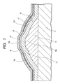
- FIG. 1 is a partial cross sectional schematic view in accordance with the first embodiment of the present invention
- FIG. 2 is a partial cross sectional schematic view for describing the second embodiment of the present invention
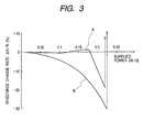
- FIG. 3 is a diagram showing the resistance value change characteristic of a heat resistor in the case of with and without thermal insulation layer in accordance with the present invention
- a thermal head of the first embodiment of the present invention is provided with a glaze layer 12 having an approximately semicircle cross section comprising a glass glaze with the film thickness of 30 to 80 ⁇ m formed on the top face of a radiative substrate 11 consisting of alumina as shown in FIG. 1.
- a convex 12a having an approximately trapezoidal cross section having a height of approximately 5 ⁇ m is formed by means of the photolithographic technique.
- a thermal insulation layer 13 comprising an organic thermal insulation layer 14 and an inorganic high thermal insulation layer 15 is formed.
- the organic thermal insulation layer 14 having a film thickness of 10 to 30 ⁇ m consists of polyimide resin deposited by means of evaporation deposition technique.
- the thermal diffusivity of the organic thermal insulation layer 14 is very small as approximately 0.11 mm 2 /sec, that is, approximately 1/4 in comparison with the glaze layer 12 having a thermal diffusivity of approximately 0.45 mm 2 /sec.
- the material is the best material for thermal insulation currently. However, the highest serviceable temperature of the organic thermal insulation layer 14 is approximately 500 °C.
- the inorganic high thermal insulation layer 15 having a thickness of 5 to 20 ⁇ m formed on the top face of the organic insulation layer 14 consists of complex oxide ceramic containing Si, a plurality of transition metals, and oxygen.
- a plurality of several transition metals are selected from among the plurality of transition metals including, for example, Ta, W, Cr, Ti, Zr, Mo, Nb, Hf, V, Fe, Ni, and Co.
- the inorganic high thermal insulation layer 15 may consist of complex nitride ceramic formed of Si, a plurality of transition metals, and nitrogen.
- thermal diffusivity of such inorganic high thermal insulation layer 15 ranges from 0.3 to 0.5 mm 2 /sec.
- a resistor layer consisting of high melting point cermet such as Ta-SiO 2 having a thickness of approximately 0.3 ⁇ m is formed on the top face of the insulation layer 13 comprising the organic thermal insulation layer 14 and the inorganic high thermal insulation layer 15 by means of sputtering, and 'the resistor layer is patterned by means of the photolithographic technique to form a plurality of heating resistors 16.
- a heating element 16a of the heating resistor 16 is formed between a common electrode 17a and an individual electrode 17b, which will be described hereinafter.
- the temperature of the heating element 16a rises to 400 to 500 °C during printing, which temperature is close to the limit of thermally endurable temperature of the organic thermal insulation layer 14. At that time, the temperature of the organic thermal insulation layer 14 is thermally protected by the inorganic high thermal insulation layer 15 and the temperature rising is suppressed, and the polyimide resin of the organic thermal insulation layer 14 will not be damaged.
- the power supplier 17 comprising the common electrode 17a and individual electrode 17b formed by patterning electrode material consisting of aluminum, copper, or gold deposited so as to have a thickness of 1 to 2 ⁇ m by means of the photolithographic technique is provided on the top face of the heating resistor 16.
- an outside-connection terminal (not shown in the drawing) is formed on the electrodes 17a and 17b so as to supply electric energy to the electrodes 17a and 17b to heat the heating element 16a.
- an oxidation resistant and wear resistant protection layer 18 consisting of Si-Al-O-N covers the respective top faces of the heating resistor 16 and the electrodes 17a and 17b.
- the glaze layer 12 is formed on the radiative substrate 11 by means of sputtering so as to form the convex 12a having a thickness of approximately 5 ⁇ m projectingly by means of the photolithographic technique in the first process.
- the thermal insulation layer 13 is formed on the radiative substrate 11 in the first step.
- the organic thermal insulation layer 14 having a film thickness of 10 to 30 ⁇ m consisting of polyimide is formed by means of evaporation polymerization technique on the radiative substrate 11 including the glaze layer 12 in the state that the radiative substrate 11 is being heated to a temperature of approximately 200 °C.
- the organic thermal insulation layer 14 is subjected to heat treatment at a temperature of 400 to 500 °C, that is a temperature near the thermally damaging temperature to stabilize the film quality of the organic thermal insulation layer 14 and to increase the adhesion between the radiative substrate 11 and the glaze layer 12.
- the top face of the heat-treated organic thermal insulation layer 14 is subjected to oxygen or nitrogen reactive sputtering by use of a sputtering target comprising a sintered material consisting of Si and a plurality of transition metals or silicide under the condition in which the sputtering film forming pressure is set as high range as 1.0 Pa to 3.0 Pa.
- a sputtering target comprising a sintered material consisting of Si and a plurality of transition metals or silicide under the condition in which the sputtering film forming pressure is set as high range as 1.0 Pa to 3.0 Pa.
- the inorganic high thermal insulation layer 15 comprising columnar crystals having a thickness of 1 to 10 ⁇ m consisting of complex oxide ceramic or complex nitride ceramic is laminated, and the first process is brought to an end.
- the high melting point cermet heating resistor 16 having a film thickness of approximately 0.3 ⁇ m consisting of Ta-SiO 2 formed by means of sputtering in a temperature range from 100 to 300 °C is formed on the top face of the thermal insulation layer 13.
- the common electrode 17a and the individual electrode 17b of the power supplier 17 are formed on the top face of the heating resistor 16 by means of sputtering and photolithographic technique respectively.
- the protection layer 18 for covering the surface of the heating resistor 16 and the power supplier 17 is formed.
- a current is supplied to the individual electrode 17b of the thermal head as described hereinabove selectively based on the printing information to thereby heat the heating element 16a of the heating resistor 16 selectively, and to thereby color thermosensitive paper or transfer ink of an ink ribbon onto plain paper. As the result, a desired high quality character or desired high quality image is printed.
- a high temperature heat treatment process applied at a temperature of 500 to 800 °C to stabilize the heating resistor 16 as described in the related art is omitted in the method for manufacture of a thermal head of the present invention.
- the element contained in the inorganic high thermal insulation layer 15, for example, Si, oxygen, or nitrogen diffuses into the heating resistor 16 when the heating resistor 16 is heated, and functions to increase the resistance ratio of the heating resistor 16 because the underlayer of the heating resistor 16 comprises the inorganic high thermal insulation layer 15.
- the stabilization heat treatment process to be applied to the heating resistor 16 can be omitted in the case of the method for manufacture of a thermal head in accordance with the present invention.
- the relation between the supplied power and the resistance change rate of the heating resistor 16 that has been manufactured without the stabilization heat treatment process is obtained by means of the step stress test (SST), and the obtained result is shown in FIG. 3.
- the curve B shown in FIG. 3 is obtained by applying the SST in the case where the heating resistor 16 is formed (not shown in the drawing) directly on the top face of the glaze layer 12, and it is found that the resistance change rate changes toward the negative side sharply and the resistance value drops sharply concomitantly with the supplied power increase (the heating temperature rises) .
- the increased resistance change rate as shown in the case of the curve B causes increased resistance value drop of the heating resistor 16 and lowered temperature of the heater 16a when the heating density of the printing is high, and results in the low printing density.
- the resistance value drop of the heating element 16a decreases and the temperature of the heater 16a increases to result in the high printing density when the heating density for printing is low.
- the printing density changes irregularly depending on the magnitude of the printing density, and the irregular printing density change results in poor printing quality.
- the curve A shown in FIG. 3 is obtained.
- the resistance value will not drop even though the supplied power is increased in the range lower than 0.15 W/d, namely practically used supplied power range, and the temperature of the heating resistor 16 is increased.
- the curve A shows the flat mode that is equivalent to the curve obtained in the case of a conventional thermal head that has been subjected to high temperature stabilization heat treatment.
- the thermal head manufactured according to the method of the present invention does not cause the problem though the high temperature heat treatment of the heating resistor 16 is omitted.
- the glaze layer 12 is not formed and the thermal insulation layer 13 having a convex on a part of the thermal insulation layer 13 is formed directly on the substrate 11.
- FIG. 2 shows the second embodiment of the present invention.
- a convex 21a is monolithically formed directly to form the top face of a radiative substrate 21 comprising a single crystal silicon wafer or metal plate by means of photolithographic technique, polishing technique, or pressing technique.
- a thermal insulation layer 23 comprising an organic thermal insulation layer 24 and an inorganic high thermal insulation layer 25, which are the same as used in the first embodiment, is formed on the radiative substrate 21, and a heating resistor 26, a power supplier 27, and a protection layer 28 are laminated on the top face of the thermal insulation layer 23. These components forms the thermal head in accordance with the second embodiment.
- the method for manufacture of the thermal head in accordance with the second embodiment will be described hereunder.
- the same manufacture method for manufacturing the thermal head in accordance with the first embodiment is used in the second embodiment excepting that the glaze layer 12 is not formed but the convex 21a is formed monolithically on the radiative substrate 21.
- the description of the manufacture process is omitted excepting the different point.
- the glaze layer 12 described in the first embodiment is unnecessary, and the manufacture process is simplified.
- FIG. 4 is a partial cross sectional view of the third embodiment of the present invention
- FIG. 5 is a partial cross sectional view of the fourth embodiment of the present invention
- FIG.8 is a view of thermal characteristics of the thermal head of the third and fourth embodiments of the present invention.
- a thermal head in accordance with the third embodiment is provided with a glaze thermal insulation layer 32 having a thickness of 30 to 80 ⁇ m consisting of glass formed on the entire or partial top face of a radiative substrate 31 consisting of alumina as shown in FIG. 4.
- a convex 32a having the cross section in the form of trapezoid ridge having a height of 5 to 15 ⁇ m is formed projectingly on the top face of the glaze thermal insulation layer 32.
- An organic thermal insulation layer 33 that functions as a thermal insulation layer consisting of heat resistant polyimide resin having a thickness of 10 to 30 ⁇ m is formed on the entire top face of the radiative substrate 31 including the convex 32a of the of the glaze thermal insulation layer 32.
- the organic thermal insulation layer 33 is formed by means of vacuum evaporation polymerization technique.
- the radiative substrate 31 is heated to a temperature of approximately 200 °C with exhaustion of the internal of a vacuum chamber, and gasified two component monomers used to form polyimide resin is then introduced to cause chemical reaction in the vacuum chamber.
- the organic thermal insulation layer 33 having the even thickness is formed as a laminate so as to have the same configuration as that of the top face of the radiative substrate 31.
- the laminate film is subjected to heat treatment at a temperature of 400 to 600 °C to complete the reaction of un-reacted components or to remove un-reacted components.
- a high heat resistant organic thermal insulation layer 33 containing less residual gas to be degassed is formed.
- a polyimide film having a thickness of 10 to 30 ⁇ m as the organic thermal insulation layer 33 with using several tens gram of raw material monomer by applying evaporation polymerization technique.
- a polyimide film to be used as the organic thermal insulation layer 33 can be formed at a reduced material cost.
- the thermal diffusivity of the organic thermal insulation layer 33 is as low as approximately 0.11 mm 2 /sec in comparison with the thermal diffusivity of the glaze thermal insulation layer 32 of approximately 0. 45 mm 2 /sec, namely approximately 1/4 of the glaze thermal insulation layer 32.
- the heat generated from the heating element 36a that will be described hereinafter, is accumulated in the organic thermal insulation layer 33, and the heat transfer to the radiative substrate 31 can be suppressed. As the result, the temperature drop of the heating element 36a is reduced during printing and the high quality printing is realized.
- an inorganic thermal insulation layer 34 having a thickness of 5 to 20 ⁇ m consisting of the combination of Si, transition metal, and oxygen, or complex oxide of nitrogen, or nitride ceramic is formed to thermally reinforce the polyimide resin.
- the thermal diffusivity of the inorganic thermal insulation layer 34 is as low as 0.3 to 0.5 mm 2 /sec that is excellent in thermal insulation.
- the inorganic thermal insulation layer 34 is a ceramic layer that contains free active transition metal and adheres firmly on the underlayer.
- a high insulating inorganic protection layer 35 having a thickness of 0.1 to 1 ⁇ m consisting of SiO 2 , SiC, Si-Al-O, Al 2 O 3 , or AlN is formed to protect the inorganic thermal insulation layer 34 mechanically and chemically.
- a plurality of heating resistors 36 consisting of high melting point cermet such as Ta-SiO 2 is formed in the form of pattern.
- the heating resistor 36 is subjected to stabilization anneal treatment at a temperature of at least 400 °C or higher.
- a power supplier 37 which comprises an common electrode 37a and individual electrode 37b, having a thickness of approximately 1 to 2 ⁇ m consisting of metal such as Al, Cu, or Au is formed to supply the electric power to the heating resistor 36.
- the heating element 36a is formed in the dot fashion.
- a wear resistance layer 38 having a thickness of approximately 5 ⁇ m consisting of Si-O-N or Si-Al-O-N is laminated to cover the respective underlayers. As the result, a high efficiency thermal head is manufactured.
- the thermal head having the structure as described hereinabove is excellent in heat accumulation performance because the four layers including the inorganic thermal insulation layer comprising the glaze thermal insulation layer 32, the organic thermal insulation layer 33 consisting of polyimide resin, the inorganic thermal insulation layer 34, and the inorganic protection layer 35 are formed to form a laminate in the order from the bottom between the radiative substrate 31 and the heating resistor 36.
- the temperature drop of the heating element 36a is reduced during printing, and the high quality printing is realized.
- the electric energy to be supplied to the heating resistor 36 can be reduced, and it is possible to realize a power-saving portable type thermal printer provided with a thermal head of the present invention, and the long battery life is realized.
- the radiative substrate 31 consisting of alumina is described in the third embodiment of the present invention, but in the fourth embodiment of the present invention, a thermal head may be provided with a radiative substrate 31 formed of single crystal Si or a metal plate, which is highly heat radiative, having no glaze thermal insulation layer 32 as shown in FIG. 5.
- the radiative substrate 31 is formed of single crystal Si or a metal plate, it is possible to form a convex 31a directly on the radiative substrate 31 by means of photolithographic technique, polishing technique, or pressing technique as shown in FIG. 5.
- the thermal head of other embodiments of the present invention can be manufactured easily, and the time required for manufacture of the thermal head is shortened.
- the thermal head described in the fourth embodiment of the present invention is excellent in heat accumulation performance because the three layers comprising the organic thermal insulation layer 33 consisting of polyimide resin, the inorganic thermal insulation layer 34, and the inorganic protection layer 35 are formed to form a laminate in the order from the bottom between the radiative substrate 31 and the heating resistor 36.
- FIG. 6 is a partial cross sectional view showing the structure of the thermal head in accordance with the fifth embodiment of the present invention
- FIG. 7 is a plan view of the thermal head.
- 41 denotes a substrate consisting of alumina or single crystal silicon
- a glaze thermal insulation layer 42 having a thickness of 40 to 70 ⁇ m consisting of glass is formed on the top face of the substrate 41.
- the glaze thermal insulation layer 42 may have a cross section in the form of approximately trapezoidal convex having a height of 30 to 80 ⁇ m as in the case of the thermal head described in the first and third embodiments.
- a heating resistor 44 consisting of Ta-SiO 2 is formed on the top face of the organic thermal insulation layer 43.
- the heating element 44a formed on a part of the heating resistor 44 is formed with a forming pitch A between adjacent heating elements 44a of 99.2 ⁇ m for obtaining 256 dpi resolution so that small dots are printed as shown in, for example, FIG. 8, and the size B in the arranging direction of the heating elements 44a is formed with a forming pitch B of 42 ⁇ m (42 % of the forming pitch A) for obtaining 600 dpi resolution.
- the size B of the heating resistor 44 is formed with the forming pitch of 31.75 ⁇ m (32 % of the forming pitch A).
- the size C in the direction that is orthogonal to the arrangement of the heating elements 44a is formed so that the aspect ratio is in the range from 0.8 to 1.5 with respect to the size B in the arrangement direction to print clear dots.
- a thermal diffusion layer 48 having a thickness of 0.1 to 1.0 ⁇ m consisting of high melting point metal such as Ti is formed.
- the thermal diffusion layer 48 has a width slightly wider than the size C of the heating element 44a and is laminated in the longitudinal direction of the arrangement of the heating elements 44a on the top face of the area on which the heating resistor 44 is formed as shown with chain double-dashed lines in FIG. 8.
- a protection layer 49 having a thickness of 5 to 10 ⁇ m consisting of Si-O-N or Si-Al-O-N is laminated to prevent oxidation and wearing of the heating resistor 44, the individual electrode 45, and the common electrode 46.
- the thermal head having the structure as described hereinabove, because the heat generated from the heating element 44a when a current is supplied to the individual electrode 45 and the common electrode 46 is dissipated quickly in the areal direction (horizontal direction) through the thermal diffusion layer 48, it is possible to print a signal dot surely even in the initial stage at the starting of printing, and a high resolution print image can be obtained.
- the thermal head having the heating element 44a with a small forming size can retain sufficient thermal energy between adjacent heating elements 44a and 44a when a suitable electric energy is supplied to the heating element 44a, the dot diameter of a dot that is printed is widen, the space between dots is covered with printing, and the sufficient printing density is obtained as a whole.
- FIG. 9 is a partial cross sectional view showing the structure.
- the sixth embodiment is different from the abovementioned fifth embodiment in that the positional relation of the heating resistor 44 and the thermal diffusion layer 48 is different each other.
- the thermal diffusion layer 48 is formed on the top face of the organic thermal insulation layer 33, and the heating resistor 44, the common electrode 45, and the individual electrode 46 are formed on the top face of the thermal diffusion layer 48 with interposition of the electric insulation layer 47.
- the thermal head of the sixth embodiment having the structure as described hereinabove can provide the same effect as provided by the thermal head in accordance with the fifth embodiment.
- the thermal head of the present invention is manufactured according to a method in which heat resistant resin is used as the material of the thermal insulation layer, many heating resistors are formed on the top face of the organic thermal insulation layer, and the thermal diffusion layer is formed on the top face of the heating resistor with interposition of the electric insulation film, or the thermal diffusion layer is formed on the bottom face of the heating resistor with interposition of the electric insulation layer.
- the energy saving thermal head is realized, and the heat generated from the heating resistor by supplying a current to the individual electrode and the common electrode is dissipated quickly in the areal direction (horizontal direction) through the thermal diffusion layer.
- the dot diameter of a dot to be printed is widen by supplying a suitable amount of electric energy to the heating resistor as required and the space between dots is covered with printing, and the sufficient printing density is obtained as a whole by use of the thermal head having the heating resistor with a small forming size to obtain a high resolution printed image. As the result, the high quality printed image can be obtained.
Landscapes
- Electronic Switches (AREA)
Abstract
Description
Claims (10)
- A thermal head provided with a thermal insulation layer formed on a radiative substrate, a plurality of heating resistor elements formed on a top face of the thermal insulation layer, a power supplier comprising an individual electrode and a common electrode connected to the heating resistor elements to supply power to the heating resistor, and a protection layer that covers surfaces of at least the heating resistor elements and the power supplier, wherein the thermal insulation layer is formed by laminating an inorganic thermal insulation layer consisting of ceramic mainly containing Si, transition metal, and oxygen and/or nitrogen on an organic thermal insulation layer consisting of polyimide resin.
- A thermal head provided with a thermal insulation layer formed on a radiative substrate, a plurality of heating resistor elements formed on the top face of the thermal insulation layer, a power supplier comprising an individual electrode and a common electrode connected to the heating resistor elements to supply power to the heating resistor, and a protection layer that covers surfaces of at least the heating resistor elements and the power supplier, wherein the thermal insulation layer is formed by laminating an inorganic thermal insulation layer consisting of ceramic mainly containing Si, transition metal, and oxygen and/or nitrogen on an organic thermal insulation layer consisting of polyimide, wherein an inorganic protection layer consisting of oxide of Si or Al, or nitride, or carbide is additionally formed on a top face of the inorganic thermal insulation layer, and wherein the heating elements are formed on a top face of the inorganic protection layer.
- The thermal head according to claim 1 or 2, wherein an organic thermal insulation layer consisting of glaze is additionally formed on a bottom face of the organic thermal insulation layer.
- The thermal head according to claim 1 or 2, wherein a film thickness of the organic thermal insulation layer is in a range from 10 to 30 µm.
- The thermal head according to claim 2, wherein a film thickness of the inorganic high insulation thermal protection layer is in a range from 5 to 20 µm.
- A thermal head provided with a thermal insulation layer formed on a radiative substrate, a plurality of heating resistor elements formed on a top face of the thermal insulation layer, a power supplier comprising an individual electrode and a common electrode connected to the heating resistor elements to supply power to the heating resistor, and a protection layer that covers surfaces of at least the heating resistor elements and the power supplier, wherein the thermal insulation layer is formed by laminating an inorganic thermal insulation layer consisting of ceramic mainly containing Si, transition metal, and oxygen and/or nitrogen on an organic thermal insulation layer consisting of polyimide resin, and wherein the protection layer is formed with a ceramic film consisting of the same material as that of the inorganic thermal insulation layer.
- The thermal head according to claim 6, wherein a film thickness of the inorganic thermal insulation layer is in a range from 5 to 20 µm, and a film thickness of the protection layer is in a range from 1 to 3 µm.
- A thermal head provided with a thermal insulation layer formed on a radiative substrate, a plurality of heating resistor elements formed on a top face of the thermal insulation layer, a power supplier comprising an individual electrode and a common electrode connected to the heating resistor elements to supply power to the heating resistor, and a protection layer that covers surfaces of at least the heating resistor elements and the power supplier, wherein the thermal insulation layer comprises an organic thermal insulation layer consisting of polyimide resin, and wherein a thermal diffusion layer is formed on a top face of the heating resistor elements with interposition of an electric insulation film.
- A thermal head provided with a thermal insulation layer formed on a radiative substrate, a plurality of heating resistor elements formed on a top face of the thermal insulation layer, a power supplier comprising an individual electrode and a common electrode connected to the heating resistor elements to supply power to the heating resistor, and a protection layer that covers surfaces of at least the heating resistor elements and the power supplier, wherein the thermal insulation layer comprises an organic thermal insulation layer consisting of polyimide resin, and wherein a thermal diffusion layer is formed on the bottom faces of the heating resistor elements with interposition of an electric insulation film.
- The thermal head according to claim 8 or 9, wherein the thermal diffusion layer consists of high melting point metal.
Applications Claiming Priority (6)
| Application Number | Priority Date | Filing Date | Title |
|---|---|---|---|
| JP2001019940A JP2002225323A (en) | 2001-01-29 | 2001-01-29 | Thermal head and its manufacturing method |
| JP2001019940 | 2001-01-29 | ||
| JP2001089453 | 2001-03-27 | ||
| JP2001089453A JP2002283603A (en) | 2001-03-27 | 2001-03-27 | Thermal head |
| JP2001117205A JP2002307732A (en) | 2001-04-16 | 2001-04-16 | Thermal head |
| JP2001117205 | 2001-04-16 |
Publications (2)
| Publication Number | Publication Date |
|---|---|
| EP1226951A2 true EP1226951A2 (en) | 2002-07-31 |
| EP1226951A3 EP1226951A3 (en) | 2003-03-12 |
Family
ID=27345835
Family Applications (1)
| Application Number | Title | Priority Date | Filing Date |
|---|---|---|---|
| EP02250258A Withdrawn EP1226951A3 (en) | 2001-01-29 | 2002-01-15 | Power-saving thermal head |
Country Status (2)
| Country | Link |
|---|---|
| US (1) | US7046265B2 (en) |
| EP (1) | EP1226951A3 (en) |
Families Citing this family (8)
| Publication number | Priority date | Publication date | Assignee | Title |
|---|---|---|---|---|
| JP2005254506A (en) * | 2004-03-09 | 2005-09-22 | Fuji Photo Film Co Ltd | Thermal head and thermal printer |
| JP2008126512A (en) * | 2006-11-20 | 2008-06-05 | Sony Corp | Thermal head and method for manufacturing thermal head |
| CN102076502B (en) * | 2008-06-26 | 2014-04-23 | 京瓷株式会社 | Recording head and recording apparatus provided with said recording head |
| JP5210090B2 (en) * | 2008-08-29 | 2013-06-12 | キヤノン株式会社 | Thermal head and thermal printer |
| JP5825778B2 (en) * | 2010-12-10 | 2015-12-02 | ローム株式会社 | Thermal print head |
| JP7541434B2 (en) * | 2019-06-14 | 2024-08-28 | ローム株式会社 | Thermal printhead and method for manufacturing the same |
| JP7269802B2 (en) | 2019-06-25 | 2023-05-09 | ローム株式会社 | Thermal print head and manufacturing method thereof |
| JP7297564B2 (en) * | 2019-07-03 | 2023-06-26 | ローム株式会社 | Thermal print head and manufacturing method thereof |
Family Cites Families (14)
| Publication number | Priority date | Publication date | Assignee | Title |
|---|---|---|---|---|
| US4096510A (en) * | 1974-08-19 | 1978-06-20 | Matsushita Electric Industrial Co., Ltd. | Thermal printing head |
| JPS52100245A (en) | 1976-02-19 | 1977-08-23 | Oki Electric Ind Co Ltd | Thermal head of high heat efficiency |
| JPS59225971A (en) * | 1983-06-06 | 1984-12-19 | Hitachi Ltd | Thermal recording head |
| JPH0649375B2 (en) * | 1985-06-27 | 1994-06-29 | 京セラ株式会社 | Thermal head and method for producing the same |
| EP0251036B1 (en) * | 1986-06-25 | 1991-05-08 | Kabushiki Kaisha Toshiba | Thermal head |
| US5157107A (en) * | 1987-01-31 | 1992-10-20 | Kabushiki Kaisha Toshiba | Heat-resistant insulating coating material and thermal head making use thereof |
| US4963893A (en) * | 1988-03-28 | 1990-10-16 | Kabushiki Kaisha Toshiba | Heat-resistant insulating substrate, thermal printing head, and thermographic apparatus |
| JPH0626914B2 (en) * | 1988-10-31 | 1994-04-13 | 株式会社東芝 | Thermal head |
| US5157414A (en) * | 1989-09-08 | 1992-10-20 | Hitachi, Ltd. | Thick film type thermal head and thermal recording device |
| JP2862637B2 (en) * | 1990-06-01 | 1999-03-03 | 株式会社東芝 | Manufacturing method of thermal head |
| JPH06238933A (en) * | 1992-07-03 | 1994-08-30 | Hitachi Koki Co Ltd | Thermal print head and thermal printer |
| WO1995035213A1 (en) * | 1994-06-21 | 1995-12-28 | Rohm Co., Ltd. | Thermal printing head, substrate used therefor and method for producing the substrate |
| JPH08267806A (en) | 1995-03-31 | 1996-10-15 | Kyocera Corp | Thermal head |
| JPH09309218A (en) * | 1996-05-22 | 1997-12-02 | Tdk Corp | Thermal head |
-
2002
- 2002-01-15 EP EP02250258A patent/EP1226951A3/en not_active Withdrawn
- 2002-01-28 US US10/058,815 patent/US7046265B2/en not_active Expired - Fee Related
Also Published As
| Publication number | Publication date |
|---|---|
| US7046265B2 (en) | 2006-05-16 |
| US20020158959A1 (en) | 2002-10-31 |
| EP1226951A3 (en) | 2003-03-12 |
Similar Documents
| Publication | Publication Date | Title |
|---|---|---|
| JP3069247B2 (en) | Thermal head | |
| KR100225259B1 (en) | Thermal printing head substrate used therefor and method for producing the substrate | |
| US7046265B2 (en) | Power-saving thermal head | |
| US8256099B2 (en) | Manufacturing method for a thermal head | |
| US6529224B2 (en) | Thermal head enabling continuous printing without print quality deterioration | |
| JP4336593B2 (en) | Thermal head | |
| EP2327554B1 (en) | Thermal head, manufacturing method therefor, and printer | |
| US6812944B2 (en) | Thermal head | |
| US6501497B2 (en) | Thermal head with small size of steps of protective layer formed on heating portion and manufacturing method thereof | |
| KR100237588B1 (en) | Thermal head and manufacturing method of the same | |
| US5477266A (en) | Thermal head, manufacturing method, and thermal printer using the thermal head | |
| US6201558B1 (en) | Thermal head | |
| US20090207229A1 (en) | Thermal print head and method for manufacturing same | |
| US20050052501A1 (en) | Heater for inkjet printer head and method for production thereof | |
| JPH10100460A (en) | Thermal head and production thereof | |
| JP2004155160A (en) | Thermal head and its manufacturing process | |
| US6330014B1 (en) | Thermal head manufactured by sequentially laminating conductive layer, layer insulating layer and heater element on heat insulating layer | |
| JP3298794B2 (en) | Thermal head and method of manufacturing the same | |
| JP4668637B2 (en) | Thermal head and manufacturing method thereof | |
| JP2002225323A (en) | Thermal head and its manufacturing method | |
| US7692676B1 (en) | Thermal head | |
| JPH07205465A (en) | Thermal head and manufacture thereof | |
| JPH06135030A (en) | Thermal head | |
| JP2010179551A (en) | Thermal head and method for manufacturing the same | |
| JPH0890809A (en) | Thermal head and manufacture thereof |
Legal Events
| Date | Code | Title | Description |
|---|---|---|---|
| PUAI | Public reference made under article 153(3) epc to a published international application that has entered the european phase |
Free format text: ORIGINAL CODE: 0009012 |
|
| AK | Designated contracting states |
Kind code of ref document: A2 Designated state(s): AT BE CH CY DE DK ES FI FR GB GR IE IT LI LU MC NL PT SE TR |
|
| AX | Request for extension of the european patent |
Free format text: AL;LT;LV;MK;RO;SI |
|
| 17P | Request for examination filed |
Effective date: 20020605 |
|
| PUAL | Search report despatched |
Free format text: ORIGINAL CODE: 0009013 |
|
| AK | Designated contracting states |
Kind code of ref document: A3 Designated state(s): AT BE CH CY DE DK ES FI FR GB GR IE IT LI LU MC NL PT SE TR Designated state(s): AT BE CH CY DE DK ES FI FR GB GR IE IT LI LU MC NL PT SE TR |
|
| AX | Request for extension of the european patent |
Extension state: AL LT LV MK RO SI |
|
| STAA | Information on the status of an ep patent application or granted ep patent |
Free format text: STATUS: THE APPLICATION HAS BEEN WITHDRAWN |
|
| 18W | Application withdrawn |
Effective date: 20030429 |