EP1225621A1 - Method of etching - Google Patents
Method of etching Download PDFInfo
- Publication number
- EP1225621A1 EP1225621A1 EP00954910A EP00954910A EP1225621A1 EP 1225621 A1 EP1225621 A1 EP 1225621A1 EP 00954910 A EP00954910 A EP 00954910A EP 00954910 A EP00954910 A EP 00954910A EP 1225621 A1 EP1225621 A1 EP 1225621A1
- Authority
- EP
- European Patent Office
- Prior art keywords
- etching
- process chamber
- gas
- wafer
- mtorr
- Prior art date
- Legal status (The legal status is an assumption and is not a legal conclusion. Google has not performed a legal analysis and makes no representation as to the accuracy of the status listed.)
- Granted
Links
Images


Classifications
-
- H—ELECTRICITY
- H10—SEMICONDUCTOR DEVICES; ELECTRIC SOLID-STATE DEVICES NOT OTHERWISE PROVIDED FOR
- H10P—GENERIC PROCESSES OR APPARATUS FOR THE MANUFACTURE OR TREATMENT OF DEVICES COVERED BY CLASS H10
- H10P50/00—Etching of wafers, substrates or parts of devices
- H10P50/20—Dry etching; Plasma etching; Reactive-ion etching
- H10P50/24—Dry etching; Plasma etching; Reactive-ion etching of semiconductor materials
- H10P50/242—Dry etching; Plasma etching; Reactive-ion etching of semiconductor materials of Group IV materials
-
- H—ELECTRICITY
- H10—SEMICONDUCTOR DEVICES; ELECTRIC SOLID-STATE DEVICES NOT OTHERWISE PROVIDED FOR
- H10W—GENERIC PACKAGES, INTERCONNECTIONS, CONNECTORS OR OTHER CONSTRUCTIONAL DETAILS OF DEVICES COVERED BY CLASS H10
- H10W20/00—Interconnections in chips, wafers or substrates
- H10W20/01—Manufacture or treatment
- H10W20/071—Manufacture or treatment of dielectric parts thereof
- H10W20/081—Manufacture or treatment of dielectric parts thereof by forming openings in the dielectric parts
-
- H—ELECTRICITY
- H10—SEMICONDUCTOR DEVICES; ELECTRIC SOLID-STATE DEVICES NOT OTHERWISE PROVIDED FOR
- H10P—GENERIC PROCESSES OR APPARATUS FOR THE MANUFACTURE OR TREATMENT OF DEVICES COVERED BY CLASS H10
- H10P50/00—Etching of wafers, substrates or parts of devices
- H10P50/20—Dry etching; Plasma etching; Reactive-ion etching
- H10P50/28—Dry etching; Plasma etching; Reactive-ion etching of insulating materials
- H10P50/286—Dry etching; Plasma etching; Reactive-ion etching of insulating materials of organic materials
- H10P50/287—Dry etching; Plasma etching; Reactive-ion etching of insulating materials of organic materials by chemical means
-
- H—ELECTRICITY
- H10—SEMICONDUCTOR DEVICES; ELECTRIC SOLID-STATE DEVICES NOT OTHERWISE PROVIDED FOR
- H10P—GENERIC PROCESSES OR APPARATUS FOR THE MANUFACTURE OR TREATMENT OF DEVICES COVERED BY CLASS H10
- H10P14/00—Formation of materials, e.g. in the shape of layers or pillars
- H10P14/60—Formation of materials, e.g. in the shape of layers or pillars of insulating materials
- H10P14/68—Organic materials, e.g. photoresists
- H10P14/683—Organic materials, e.g. photoresists carbon-based polymeric organic materials, e.g. polyimides, poly cyclobutene or PVC
-
- H—ELECTRICITY
- H10—SEMICONDUCTOR DEVICES; ELECTRIC SOLID-STATE DEVICES NOT OTHERWISE PROVIDED FOR
- H10P—GENERIC PROCESSES OR APPARATUS FOR THE MANUFACTURE OR TREATMENT OF DEVICES COVERED BY CLASS H10
- H10P14/00—Formation of materials, e.g. in the shape of layers or pillars
- H10P14/60—Formation of materials, e.g. in the shape of layers or pillars of insulating materials
- H10P14/68—Organic materials, e.g. photoresists
- H10P14/683—Organic materials, e.g. photoresists carbon-based polymeric organic materials, e.g. polyimides, poly cyclobutene or PVC
- H10P14/687—Organic materials, e.g. photoresists carbon-based polymeric organic materials, e.g. polyimides, poly cyclobutene or PVC the materials being fluorocarbon compounds, e.g. (CHxFy) n or polytetrafluoroethylene
-
- H—ELECTRICITY
- H10—SEMICONDUCTOR DEVICES; ELECTRIC SOLID-STATE DEVICES NOT OTHERWISE PROVIDED FOR
- H10P—GENERIC PROCESSES OR APPARATUS FOR THE MANUFACTURE OR TREATMENT OF DEVICES COVERED BY CLASS H10
- H10P14/00—Formation of materials, e.g. in the shape of layers or pillars
- H10P14/60—Formation of materials, e.g. in the shape of layers or pillars of insulating materials
- H10P14/69—Inorganic materials
- H10P14/692—Inorganic materials composed of oxides, glassy oxides or oxide-based glasses
- H10P14/6921—Inorganic materials composed of oxides, glassy oxides or oxide-based glasses containing silicon
- H10P14/6922—Inorganic materials composed of oxides, glassy oxides or oxide-based glasses containing silicon the material containing Si, O and at least one of H, N, C, F or other non-metal elements, e.g. SiOC, SiOC:H or SiONC
Definitions
- the present invention relates to a method of etching.
- the wiring pattern is formed by depositing the Al alloy by spattering on a layer insulating film and then by etching.
- the pressure in a process chamber is generally several to 100 mTorr. According to JP60-170238, the maximum etching speed can be achieved at 50-100 mTorr.
- damascene process is a method for forming the groove of wiring pattern on the layer insulating film and embedding the wiring material in the groove.
- the specific resistance becomes halved and the etching speed can be easily high by changing the wiring material from Al alloy to Cu. Since flattening can be easily achieved by Chemical Mechanical Polishing (CMP) recently, the damascene process has become easy to be utilized.
- CMP Chemical Mechanical Polishing
- the dual damascene is a technology of forming a wiring and a via hole at the same time by forming an inverted convex groove on which the wiring and the via hole are formed in the later step and by embedding metal substance for wiring in the groove.
- the inverted convex groove for the dual damascene it is necessary to control so that the bottom of the formed groove may be made flat when the etching is stopped before the etching goes through the layer insulating film.
- etch stop a layer as a ground (hereafter, referred to as an "etch stop") is formed at a desired depth.
- the etch stop has a high dielectric constant, a capacitor is formed between the wirings.
- the present invention has been achieved in views of aforementioned problems.
- the first object of the present invention is to provide a novel and improved method of etching capable of preventing micro trenching without using an etch stop.
- the second object of the present invention is to provide a novel and improved method of etching capable of improving mask selectivity.
- a method of etching for etching an organic film on a workpiece placed in a hermetically sealed process chamber filled with process gas wherein: the process gas includes at least nitrogen atoms and hydrogen atoms; and a pressure in the process chamber is substantially higher than 500 mTorr.
- the organic film is made from a low-dielectric constant material with the relative dielectric constant less than 3.5.
- the pressure in the process chamber is substantially 500-800 mTorr.
- the process gas includes at least nitrogen atoms and hydrogen atoms and a pressure in the process chamber is set substantially higher than 500 mTorr, micro trenching can be prevented without using an etch stop and mask selectivity can be improved. Therefore, the effect can be achieved especially in the process with the necessity to stop etching before the etching goes through the organic film, for example, dual damascene process and the like.
- N 2 can be adopted as the gas including nitrogen atoms and H 2 as hydrogen atoms. If N 2 and H 2 are adopted as the component of the process gas as this, the process gas can be easily treated and will not easily cause greenhouse warming even if the process gas is released to atmosphere. Furthermore, since N 2 and H 2 are cheap, the cost for process will not increase.
- the control of the groove shape can be facilitated.
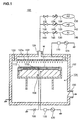
- a process chamber 104 is formed, and inside the process chamber 104, a lower electrode 106 constituting a susceptor capable of moving up and down freely is provided.
- an electrostatic chuck 110 connected to a high-voltage DC source 108 is provided, and a workpiece such as a semiconductor wafer (hereafter referred to as a "wafer") W is placed on the upper surface of the electrostatic chuck 110.
- a focus ring 112 achieving an insulating property is provided around the wafer W placed on the lower electrode 106.
- a high-frequency source 120 is connected to the lower electrode 106 via a matcher 118.
- an upper electrode 122 having numerous gas outlet holes 122a is provided.
- An insulator 123 is provided between the upper electrode 122 and the process container 102.
- a high-frequency source 121 that outputs plasma generating high-frequency power is connected to the upper electrode 122 via a matcher 119.
- a gas supply pipe 124 is connected to the gas outlet holes 122a, and in the example shown in the figure, first ⁇ third branch pipes 126, 128 and 130 are connected to the gas supply pipe 124.
- a gas supply source 136 that supplies N 2 is connected to the first branch pipe 126 via an open/close valve 132 and a flow-rate regulating valve 134.
- a gas supply source 142 that supplies H 2 is connected to the second branch pipe 128 via an open/close valve 138 and a flow-rate regulating valve 140.
- a gas supply source 148 that supplies Ar is connected to the third branch pipe 130 via an open/close valve 144 and a flow-rate regulating valve 146.
- the inert gas added into the process gas is not limited to Ar in the example above and any inert gas including He and Kr may be used instead, as long as it can be utilized to adjust the plasma excited inside the process chamber 104.
- a gas discharge pipe 150 which communicates with a vacuum drawing mechanism (not shown) is connected, and through the function of the vacuum drawing mechanism, the atmosphere inside the process chamber 104 is sustained at a specific reduced pressure.
- the wafer W used in the implementation example has a layer insulating film to undergo the etching process formed on a Cu layer.
- the layer insulating film is made from an organic material with low-dielectric constant much lower than a conventional SiO 2 film in the relative dielectric constant such as polyorganosiloxane-bridged benzocyclobutene resin (hereafter, referred to as "BCB"), DowChemical-made SiLK (trade name) and FLARE (trade name) which has the following structure.
- BCB polyorganosiloxane-bridged benzocyclobutene resin
- FLARE trade name
- an etching mask having a specific pattern is formed on the layer insulating film.
- This etching mask may be constituted of a photoresist film layer, or SiO 2 film and a photoresist film for instance.
- the wafer W is placed on the lower electrode 106 the temperature of which has been preset to a specific level, and the temperature of the wafer W is sustained at approximately 20°C ⁇ 60°C in conformance to particular requirements of the process.
- the process gas in the implementation example i.e., the process gas achieved by mixing N 2 , H 2 and Ar, is induced into the process chamber 104 while adjusting the flow rates of the individual gases through the flow-rate regulating valves 134, 140 and 146 inserted at the gas supply pipe 124.
- vacuum drawing is implemented inside the process chamber 104 to achieve a specific pressure level for the atmosphere inside the process chamber 104, which will correspond the requirements of the process, substantially at higher than 500mTorr, more preferably 500-800 mTorr.
- high-frequency power with a frequency of 2 MHz and a power level of 600-1400 W, for instance, is applied to the lower electrode 106.
- high-frequency power with a frequency of 60 MHz and a power level of 600-1400 W, for instance, is applied to the upper electrode 122.
- high density plasma is generated inside the process container 102 and contact holes achieving a specific shape are formed at the layer insulating film of wafer W constituting of an organic material with low-dielectric constant with the plasma.
- This implementation example is configured as described above. Since the process gas includes at least nitrogen atoms and hydrogen atoms under a pressure substantially higher than 500 mTorr in the process chamber, micro trenching can be prevented without using an etch stop. Mask selectivity is also improved.
- N 2 and H 2 are adopted as the component of the process gas, the process gas can be easily treated and will not easily cause greenhouse warming even if the process gas is released to atmosphere. Further, since N 2 and H 2 are cheap, the cost for process will not increase. Also, since the process gas includes Ar, the control of the groove shape can be facilitated as the etching condition can be easily controlled. Furthermore, since a specific etching process can be achieved without adding O 2 into the process gas, the oxidization of the Cu layer can be prevented during the process. Consequently, it is not necessary to form an oxidization-prevention film on the Cu film, and workpiece can be relatively thinner.
- the etching process was performed by basing on the condition as in the following table to form contact holes at the layer insulating film of the wafer W described earlier. (Table 1)
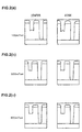
- the central part of wafer W is designated as center, the end part of wafer W as edge and the part in the middle of central and end parts as middle in the table and the drawing.
- trenching is the ratio of the depth of etching at the end part of contact holes to the depth of etching at the roughly central part of contact holes. The more the ratio becomes, the more degree of micro trenching Implement ation example Flowrate of process gas (sccm) Pressure level for atmosphere in process chamber (mTorr) Etching rate ( /m) Trenching (%) Sectional shape of contact N 2 H 2 A r center edge center edge hole 2 (a) 400 400 0 100 3063 3146 157 153 Fig.
- contact holes with good shapes can be formed without lowering the etching rate, as shown in table 1 and FIGS. 2(b) and (c).
- micro trenching is formed on the contact holes.
- implementation examples 2(a)-(c) achieved by changing the pressure level for the atmosphere inside the process chamber 104 are explained.
- the width of formed contact hole is changed under the same condition as in the implementation (Table 2) example 1.
- the etching process was performed by basing on the condition as in the following table to form contact holes at the layer insulating film of the wafer W described earlier.
- contact holes with good shapes can be formed without lowering the etching rate, as shown in table 2 and FIGS. 3(b) and (c).
- micro trenching is formed on the contact holes. Judging from the result in this implementation example, if the pressure inside the process chamber is set at a specific level, contact holes with good shapes can be formed even when the width of contact hole is changed.
- etching apparatus 200 that may adopt the method of etching in the implementation example is explained.
- a process chamber 204 is formed, and inside the process chamber 204, a lower electrode 206 constituting a susceptor capable of moving up and down freely is provided.
- an electrostatic chuck 210 connected to a high-voltage DC source 208 is provided, and a wafer W is placed on the upper surface of the electrostatic chuck 210.
- a focus ring 212 achieving an insulating property is provided around the wafer W placed on the lower electrode 206.
- a high-frequency source 220 outputting plasma generating high-frequency power is connected to the lower electrode 206 via a matcher 220.
- an upper electrode 222 having numerous gas outlet holes 222a is provided at the ceiling of the process chamber 204 facing opposite the mounting surface of the lower electrode 206.
- the upper electrode 222 composes a part of the process container 202.
- a gas supply pipe 224 is connected to the gas outlet holes 222a as the etching apparatus 100, and in the example shown in the figure, first and second branch pipes 224 and 228 are connected to the gas supply pipe 224.
- a gas supply source 236 that supplies N 2 is connected to the first branch pipe 226 via an open/close valve 232 and a flow-rate regulating valve 234.
- a gas supply source 242 that supplies H 2 is connected to the second branch pipe 228 via an open/close valve 238 and a flow-rate regulating valve 240.
- a third branch pipe may be provided to supply (Table 3) inert gas such as Ar as in the etching apparatus 100.
- a gas discharge pipe 150 as in the etching apparatus 100 is connected.
- a magnet 238 is arranged covering the outside-wall of the process container 202 outside the process chamber 204.
- a gyromagnetic field is formed in the plasma region located between the upper electrode 222 and the lower electrode 206.
- the temperature of the wafer W is sustained approximately at 20°C ⁇ 80°C.
- high-frequency power with a frequency of 13.56 MHz and a power level of 500-1500 W, for instance, is applied to the lower electrode 206
- example 3(a)-(d) the etching process was performed by basing on the condition as in the following table to form contact holes
- Implement ation example Flowrate of process gas (sccm) Etching width ( ⁇ m) Pressure level for atmosphere in process chamber (mTorr) Etching rate ( /m) Sectional shape of contact hole N 2 H 2 center middle edge 3 (a) 200 200 0.35 500 4500/ 5125 4750/ 5250 5250/ 5750 Fig. 5 (a) 3(b) 200 200 0.30 500 4875/ 5250 5000/ 5375 5000/ 5500 Fig. 5 (b) 3(c) 100 100 0.35 500 5000/ 5625 4875/ 5500 5000/ 5625 Fig. 5(c) 3(d) 100 100 0.30 500 4750/ 5250 5000/ 5625 5125/ 5500 Fig.5 (d) at the layer insulating film of the wafer W described earlier.
- contact holes with good shapes can be formed at any flow rate, as shown in table 3 and FIG. 5. Judging from the result in this implementation example, if the pressure inside the process chamber is set at a specific - level for the atmosphere, contact holes with good shapes can be formed even when the flow rate of N 2 and H 2 is changed.
- the present invention is not limited to this example.
- the present invention may be implemented by adding various kinds of gasses such as O 2 and an inert gas in the process gas constituted by mixing N 2 , H 2 and Ar.
- the present invention can be implemented using any process gas containing at least nitrogen atoms and hydrogen atoms.
- the present invention is not limited to this example and it may be adopted when performing any type of etching process on a layer insulating film formed at a workpiece.
- micro trenching can be prevented without using an etch stop.
- Mask selectivity is also improved.
- the process gas can be easily treated and will not easily cause greenhouse warming even if the process gas is released to atmosphere.
- the cost for process will not increase.
- the control of the groove shape can be facilitated as the etching condition can be easily controlled.
- the present invention may be adopted a method of etching and, in particular, it is ideal in a method of etching in which there is needed to prevent micro trenching and improve mask selectivity.
Landscapes
- Drying Of Semiconductors (AREA)
- ing And Chemical Polishing (AREA)
Abstract
Description

| Implement ation example | Flowrate of process gas (sccm) | Pressure level for atmospher e in process chamber (mTorr) | Etching rate ( /m) | Trenching (%) | Sectional shape of contact hole | ||||
| N2 | H2 | Ar | center | edge | center | edge | |||
| 1 (a) | 400 | 400 | 0 | 100 | 3958 | 4000 | 117 | 120 | Fig. 2 (a) |
| 1(b) | 400 | 400 | 0 | 500 | 3792 | 3354 | 100 | 112 | Fig. 2 (b) |
| 1(c) | 400 | 400 | 500 | 800 | 4043 | 3532 | 87 | 104 | Fig. 2(c) |
(Table 1)
| Implement ation example | Flowrate of process gas (sccm) | Pressure level for atmosphere in process chamber (mTorr) | Etching rate ( /m) | Trenching (%) | Sectional shape of contact | ||||
| N2 | H2 | Ar | center | edge | center | edge | hole | ||
| 2 (a) | 400 | 400 | 0 | 100 | 3063 | 3146 | 157 | 153 | Fig. 3 (a) |
| 2(b) | 400 | 400 | 0 | 500 | 3521 | 3146 | 114 | 126 | Fig. 3 (b) |
| 2(c) | 400 | 400 | 500 | 800 | 3638 | 3426 | 89 | 106 | Fig. 3(c) |
(Table 2)
example 1.
(Table 3)
inert gas such as Ar as in the
| Implement ation example | Flowrate of process gas (sccm) | Etching width (µm) | Pressure level for atmosphere in process chamber (mTorr) | Etching rate ( /m) | Sectional shape of contact hole | |||
| N2 | H2 | center | middle | edge | ||||
| 3 (a) | 200 | 200 | 0.35 | 500 | 4500/ 5125 | 4750/ 5250 | 5250/ 5750 | Fig. 5 (a) |
| 3(b) | 200 | 200 | 0.30 | 500 | 4875/ 5250 | 5000/ 5375 | 5000/ 5500 | Fig. 5 (b) |
| 3(c) | 100 | 100 | 0.35 | 500 | 5000/ 5625 | 4875/ 5500 | 5000/ 5625 | Fig. 5(c) |
| 3(d) | 100 | 100 | 0.30 | 500 | 4750/ 5250 | 5000/ 5625 | 5125/ 5500 | Fig.5 (d) |
- 100
- etching apparatus
- 102
- process container
- 104
- process chamber
- 106
- lower electrode
- 108
- high-voltage DC source
- 110
- electrostatic chuck
- 112
- focus ring
- 118
- matcher
- 119
- matcher
- 120
- high-frequency source
- 121
- high-frequency source
- 122
- upper electrode
- 122a
- gas outlet holes
- 123
- insulator
- 124
- gas supply pipe
- 126, 128, 130
- branch pipe (first branch pipe, second branch pipe, third branch pipe)
- 132, 138, 144
- open/close valve
- 134, 140, 146
- flow-rate regulating valve
- 136, 142, 148
- gas supply source
- 150
- gas discharge pipe
- W
- wafer
Claims (5)
- A method of etching for etching an organic film on a workpiece placed in a hermetically sealed process chamber filled with process gas wherein: the process gas includes at least nitrogen atoms and hydrogen atoms; and
a pressure in the process chamber is substantially higher than 500 mTorr. - A method of etching according to claim 1 wherein the pressure in the process chamber is substantially higher than 500 mTorr.
- A method of etching according to claim 1 wherein the nitrogen atoms constitute N2 and the hydrogen atoms constitute H2.
- A method of etching according to claim 1 wherein the process gas further includes Ar.
- A method of etching according to claim 1 wherein the etching on the organic film is stopped before the etching goes through the organic film.
Applications Claiming Priority (3)
| Application Number | Priority Date | Filing Date | Title |
|---|---|---|---|
| JP23519199 | 1999-08-23 | ||
| JP23519199A JP3844413B2 (en) | 1999-08-23 | 1999-08-23 | Etching method |
| PCT/JP2000/005623 WO2001015213A1 (en) | 1999-08-23 | 2000-08-23 | Method of etching |
Publications (3)
| Publication Number | Publication Date |
|---|---|
| EP1225621A1 true EP1225621A1 (en) | 2002-07-24 |
| EP1225621A4 EP1225621A4 (en) | 2007-03-28 |
| EP1225621B1 EP1225621B1 (en) | 2011-07-13 |
Family
ID=16982437
Family Applications (1)
| Application Number | Title | Priority Date | Filing Date |
|---|---|---|---|
| EP00954910A Expired - Lifetime EP1225621B1 (en) | 1999-08-23 | 2000-08-23 | Method of etching |
Country Status (5)
| Country | Link |
|---|---|
| EP (1) | EP1225621B1 (en) |
| JP (1) | JP3844413B2 (en) |
| KR (1) | KR100709817B1 (en) |
| TW (1) | TW469488B (en) |
| WO (1) | WO2001015213A1 (en) |
Cited By (2)
| Publication number | Priority date | Publication date | Assignee | Title |
|---|---|---|---|---|
| CN101866846B (en) * | 2009-04-14 | 2012-04-18 | 中芯国际集成电路制造(北京)有限公司 | Method for etching groove |
| US12622241B2 (en) * | 2023-01-18 | 2026-05-05 | Taiwan Semiconductor Manufacturing Company, Ltd. | Structures with convex cavity bottoms |
Families Citing this family (4)
| Publication number | Priority date | Publication date | Assignee | Title |
|---|---|---|---|---|
| JP3739325B2 (en) * | 2001-09-20 | 2006-01-25 | 株式会社日立製作所 | Etching method of organic insulating film |
| JP2004214336A (en) | 2002-12-27 | 2004-07-29 | Tokyo Electron Ltd | Plasma etching method and plasma etching apparatus |
| JP2004342873A (en) | 2003-05-16 | 2004-12-02 | Tokyo Electron Ltd | Semiconductor device and method of manufacturing the same |
| US7344993B2 (en) * | 2005-01-11 | 2008-03-18 | Tokyo Electron Limited, Inc. | Low-pressure removal of photoresist and etch residue |
Family Cites Families (10)
| Publication number | Priority date | Publication date | Assignee | Title |
|---|---|---|---|---|
| US4529860A (en) | 1982-08-02 | 1985-07-16 | Motorola, Inc. | Plasma etching of organic materials |
| JPS60170238A (en) * | 1984-02-15 | 1985-09-03 | Toyota Central Res & Dev Lab Inc | Dry etching method |
| JPH10150101A (en) * | 1996-11-15 | 1998-06-02 | Nippon Steel Corp | Semiconductor device and manufacturing method thereof |
| JPH10209118A (en) * | 1997-01-28 | 1998-08-07 | Sony Corp | Ashing method |
| US6379576B2 (en) * | 1997-11-17 | 2002-04-30 | Mattson Technology, Inc. | Systems and methods for variable mode plasma enhanced processing of semiconductor wafers |
| JPH11150101A (en) * | 1997-11-18 | 1999-06-02 | Nec Corp | Method for manufacturing semiconductor device |
| US6080680A (en) * | 1997-12-19 | 2000-06-27 | Lam Research Corporation | Method and composition for dry etching in semiconductor fabrication |
| JP2000036484A (en) * | 1998-05-11 | 2000-02-02 | Tokyo Electron Ltd | Plasma processing method |
| FR2789804B1 (en) * | 1999-02-17 | 2002-08-23 | France Telecom | ANISOTROPIC GASEOUS PLASMA ENGRAVING PROCESS OF AN ORGANIC DIELECTRIC POLYMERIC MATERIAL AND APPLICATION TO MICROELECTRONICS |
| JP4207303B2 (en) * | 1999-04-07 | 2009-01-14 | ソニー株式会社 | Semiconductor device and manufacturing method thereof |
-
1999
- 1999-08-23 JP JP23519199A patent/JP3844413B2/en not_active Expired - Fee Related
-
2000
- 2000-08-22 TW TW089116981A patent/TW469488B/en active
- 2000-08-23 EP EP00954910A patent/EP1225621B1/en not_active Expired - Lifetime
- 2000-08-23 WO PCT/JP2000/005623 patent/WO2001015213A1/en not_active Ceased
- 2000-08-23 KR KR1020027002261A patent/KR100709817B1/en not_active Expired - Fee Related
Cited By (2)
| Publication number | Priority date | Publication date | Assignee | Title |
|---|---|---|---|---|
| CN101866846B (en) * | 2009-04-14 | 2012-04-18 | 中芯国际集成电路制造(北京)有限公司 | Method for etching groove |
| US12622241B2 (en) * | 2023-01-18 | 2026-05-05 | Taiwan Semiconductor Manufacturing Company, Ltd. | Structures with convex cavity bottoms |
Also Published As
| Publication number | Publication date |
|---|---|
| EP1225621B1 (en) | 2011-07-13 |
| JP3844413B2 (en) | 2006-11-15 |
| JP2001060582A (en) | 2001-03-06 |
| KR100709817B1 (en) | 2007-04-23 |
| TW469488B (en) | 2001-12-21 |
| EP1225621A4 (en) | 2007-03-28 |
| KR20020027567A (en) | 2002-04-13 |
| WO2001015213A1 (en) | 2001-03-01 |
Similar Documents
| Publication | Publication Date | Title |
|---|---|---|
| EP1033745B1 (en) | Method for forming a barrier layer for use in a copper interconnect | |
| US6489248B2 (en) | Method and apparatus for etch passivating and etching a substrate | |
| US6465359B2 (en) | Etchant for use in a semiconductor processing method and system | |
| US6489245B1 (en) | Methods for reducing mask erosion during plasma etching | |
| EP1100119A1 (en) | Plasma processing method | |
| US20020142610A1 (en) | Plasma etching of dielectric layer with selectivity to stop layer | |
| WO2002080230A2 (en) | Method of plasma etching low-k organosilicate materials | |
| EP1374288A2 (en) | Method of plasma etching organic antireflective coating | |
| US20040106293A1 (en) | Method for etching organic insulating film and dual damasene process | |
| EP1010203B1 (en) | Method for etching a conductive layer | |
| US6488863B2 (en) | Plasma etching method | |
| EP1041613A1 (en) | Etching process | |
| US7030027B1 (en) | Etching methods and apparatus for producing semiconductor devices | |
| US6756314B2 (en) | Method for etching a hard mask layer and a metal layer | |
| EP1225621A1 (en) | Method of etching | |
| JP4388645B2 (en) | Plasma etching method | |
| JP3987637B2 (en) | Etching method | |
| US7582220B1 (en) | Etching method | |
| EP1207550B1 (en) | Method of etching and method of plasma treatment | |
| TWI894174B (en) | Method of depositing layers | |
| JP2003086568A (en) | Etching method | |
| US6461962B1 (en) | Etching method | |
| JP4550981B2 (en) | Etching method |
Legal Events
| Date | Code | Title | Description |
|---|---|---|---|
| PUAI | Public reference made under article 153(3) epc to a published international application that has entered the european phase |
Free format text: ORIGINAL CODE: 0009012 |
|
| 17P | Request for examination filed |
Effective date: 20020204 |
|
| AK | Designated contracting states |
Kind code of ref document: A1 Designated state(s): AT BE CH CY DE DK ES FI FR GB GR IE IT LI LU MC NL PT SE |
|
| RBV | Designated contracting states (corrected) |
Designated state(s): AT BE CH CY DE FR GB IT LI NL |
|
| A4 | Supplementary search report drawn up and despatched |
Effective date: 20070223 |
|
| 17Q | First examination report despatched |
Effective date: 20080116 |
|
| GRAP | Despatch of communication of intention to grant a patent |
Free format text: ORIGINAL CODE: EPIDOSNIGR1 |
|
| GRAS | Grant fee paid |
Free format text: ORIGINAL CODE: EPIDOSNIGR3 |
|
| GRAA | (expected) grant |
Free format text: ORIGINAL CODE: 0009210 |
|
| AK | Designated contracting states |
Kind code of ref document: B1 Designated state(s): DE FR GB IT NL |
|
| REG | Reference to a national code |
Ref country code: GB Ref legal event code: FG4D |
|
| REG | Reference to a national code |
Ref country code: DE Ref legal event code: R096 Ref document number: 60046212 Country of ref document: DE Effective date: 20110901 |
|
| REG | Reference to a national code |
Ref country code: NL Ref legal event code: VDEP Effective date: 20110713 |
|
| PG25 | Lapsed in a contracting state [announced via postgrant information from national office to epo] |
Ref country code: NL Free format text: LAPSE BECAUSE OF FAILURE TO SUBMIT A TRANSLATION OF THE DESCRIPTION OR TO PAY THE FEE WITHIN THE PRESCRIBED TIME-LIMIT Effective date: 20110713 |
|
| PLBE | No opposition filed within time limit |
Free format text: ORIGINAL CODE: 0009261 |
|
| REG | Reference to a national code |
Ref country code: FR Ref legal event code: ST Effective date: 20120430 |
|
| STAA | Information on the status of an ep patent application or granted ep patent |
Free format text: STATUS: NO OPPOSITION FILED WITHIN TIME LIMIT |
|
| PG25 | Lapsed in a contracting state [announced via postgrant information from national office to epo] |
Ref country code: IT Free format text: LAPSE BECAUSE OF FAILURE TO SUBMIT A TRANSLATION OF THE DESCRIPTION OR TO PAY THE FEE WITHIN THE PRESCRIBED TIME-LIMIT Effective date: 20110713 |
|
| 26N | No opposition filed |
Effective date: 20120416 |
|
| GBPC | Gb: european patent ceased through non-payment of renewal fee |
Effective date: 20111013 |
|
| REG | Reference to a national code |
Ref country code: DE Ref legal event code: R097 Ref document number: 60046212 Country of ref document: DE Effective date: 20120416 |
|
| PG25 | Lapsed in a contracting state [announced via postgrant information from national office to epo] |
Ref country code: FR Free format text: LAPSE BECAUSE OF NON-PAYMENT OF DUE FEES Effective date: 20110913 Ref country code: GB Free format text: LAPSE BECAUSE OF NON-PAYMENT OF DUE FEES Effective date: 20111013 |
|
| PGFP | Annual fee paid to national office [announced via postgrant information from national office to epo] |
Ref country code: DE Payment date: 20120816 Year of fee payment: 13 |
|
| PG25 | Lapsed in a contracting state [announced via postgrant information from national office to epo] |
Ref country code: DE Free format text: LAPSE BECAUSE OF NON-PAYMENT OF DUE FEES Effective date: 20140301 |
|
| REG | Reference to a national code |
Ref country code: DE Ref legal event code: R119 Ref document number: 60046212 Country of ref document: DE Effective date: 20140301 |