JP2004214336A - Method and apparatus for plasma etching - Google Patents
Method and apparatus for plasma etching Download PDFInfo
- Publication number
- JP2004214336A JP2004214336A JP2002380558A JP2002380558A JP2004214336A JP 2004214336 A JP2004214336 A JP 2004214336A JP 2002380558 A JP2002380558 A JP 2002380558A JP 2002380558 A JP2002380558 A JP 2002380558A JP 2004214336 A JP2004214336 A JP 2004214336A
- Authority
- JP
- Japan
- Prior art keywords
- frequency power
- plasma
- plasma etching
- processed
- material film
- Prior art date
- Legal status (The legal status is an assumption and is not a legal conclusion. Google has not performed a legal analysis and makes no representation as to the accuracy of the status listed.)
- Pending
Links
Images


Classifications
-
- H—ELECTRICITY
- H01—ELECTRIC ELEMENTS
- H01L—SEMICONDUCTOR DEVICES NOT COVERED BY CLASS H10
- H01L21/00—Processes or apparatus adapted for the manufacture or treatment of semiconductor or solid state devices or of parts thereof
- H01L21/02—Manufacture or treatment of semiconductor devices or of parts thereof
- H01L21/04—Manufacture or treatment of semiconductor devices or of parts thereof the devices having at least one potential-jump barrier or surface barrier, e.g. PN junction, depletion layer or carrier concentration layer
- H01L21/18—Manufacture or treatment of semiconductor devices or of parts thereof the devices having at least one potential-jump barrier or surface barrier, e.g. PN junction, depletion layer or carrier concentration layer the devices having semiconductor bodies comprising elements of Group IV of the Periodic System or AIIIBV compounds with or without impurities, e.g. doping materials
- H01L21/30—Treatment of semiconductor bodies using processes or apparatus not provided for in groups H01L21/20 - H01L21/26
- H01L21/31—Treatment of semiconductor bodies using processes or apparatus not provided for in groups H01L21/20 - H01L21/26 to form insulating layers thereon, e.g. for masking or by using photolithographic techniques; After treatment of these layers; Selection of materials for these layers
- H01L21/3105—After-treatment
- H01L21/311—Etching the insulating layers by chemical or physical means
- H01L21/31127—Etching organic layers
- H01L21/31133—Etching organic layers by chemical means
- H01L21/31138—Etching organic layers by chemical means by dry-etching
-
- H—ELECTRICITY
- H01—ELECTRIC ELEMENTS
- H01J—ELECTRIC DISCHARGE TUBES OR DISCHARGE LAMPS
- H01J37/00—Discharge tubes with provision for introducing objects or material to be exposed to the discharge, e.g. for the purpose of examination or processing thereof
- H01J37/32—Gas-filled discharge tubes
- H01J37/32431—Constructional details of the reactor
- H01J37/32458—Vessel
- H01J37/32522—Temperature
-
- H—ELECTRICITY
- H01—ELECTRIC ELEMENTS
- H01J—ELECTRIC DISCHARGE TUBES OR DISCHARGE LAMPS
- H01J37/00—Discharge tubes with provision for introducing objects or material to be exposed to the discharge, e.g. for the purpose of examination or processing thereof
- H01J37/32—Gas-filled discharge tubes
- H01J37/32431—Constructional details of the reactor
- H01J37/32623—Mechanical discharge control means
- H01J37/32633—Baffles
-
- H—ELECTRICITY
- H01—ELECTRIC ELEMENTS
- H01J—ELECTRIC DISCHARGE TUBES OR DISCHARGE LAMPS
- H01J37/00—Discharge tubes with provision for introducing objects or material to be exposed to the discharge, e.g. for the purpose of examination or processing thereof
- H01J37/32—Gas-filled discharge tubes
- H01J37/32431—Constructional details of the reactor
- H01J37/32623—Mechanical discharge control means
- H01J37/32642—Focus rings
-
- H—ELECTRICITY
- H01—ELECTRIC ELEMENTS
- H01J—ELECTRIC DISCHARGE TUBES OR DISCHARGE LAMPS
- H01J37/00—Discharge tubes with provision for introducing objects or material to be exposed to the discharge, e.g. for the purpose of examination or processing thereof
- H01J37/32—Gas-filled discharge tubes
- H01J37/32431—Constructional details of the reactor
- H01J37/3266—Magnetic control means
- H01J37/32688—Multi-cusp fields
-
- H—ELECTRICITY
- H01—ELECTRIC ELEMENTS
- H01J—ELECTRIC DISCHARGE TUBES OR DISCHARGE LAMPS
- H01J2237/00—Discharge tubes exposing object to beam, e.g. for analysis treatment, etching, imaging
- H01J2237/32—Processing objects by plasma generation
- H01J2237/33—Processing objects by plasma generation characterised by the type of processing
- H01J2237/334—Etching
- H01J2237/3341—Reactive etching
Abstract
Description
【0001】
【発明の属する技術分野】
本発明は、低誘電率膜(low−k膜)等の有機系材料膜が形成された半導体ウエハ等の被処理基板において、その有機系材料膜をプラズマエッチングするプラズマエッチング方法に関する。
【0002】
【従来の技術】
半導体デバイスの配線工程では、配線層間には層間絶縁膜が形成されており、配線層を導通させるために層間絶縁膜をエッチングする。この層間絶縁膜としては、近時、半導体デバイスのさらなる高速化の要求から、より低誘電率の膜が求められており、このような低誘電率膜としては有機系材料膜が用いられつつある。
【0003】
このような有機系材料膜のエッチングは、酸化シリコン等の無機系材料膜をマスクとしてプラズマエッチングにより行っている。具体的には、チャンバー内に上下に対向する一対の対向電極を設けた平行平板型のプラズマエッチング装置を用い、下部電極に半導体ウエハ(以下、単にウエハと記載する)を載置して、下部電極に周波数13.56MHzの高周波電力を供給し、処理ガスとして、N2、H2、Ar等が用いられている(特許文献1,2)。
【0004】
【特許文献1】
特開2001−60582公報(特許請求の範囲、段落0022〜0024等)
【特許文献2】
特開2001−118825公報(特許請求の範囲、段落0015、0022等)
【0005】
【発明が解決しようとする課題】
しかしながら、上記特許文献1,2に示すような従来のエッチング条件で有機系材料膜をエッチングする場合には、高エッチングレートを得るためにプラズマ密度を上げると自己バイアス電圧も同時に上昇するため、引き込まれたイオンにより例えばマスクとして有機系材料膜に隣接して設けられた無機系材料膜の肩落ちが激しくなり、無機系材料膜に対する有機系材料膜のエッチング選択比が低下してしまい、高エッチングレートと高エッチング選択比を両立することができない。
【0006】
また、このような肩落ちを防止して高選択比で有機系材料膜をエッチングするために、エッチング作用の強い(スパッタ作用の強い)Arガスのような原子ガスを除いて分子性の単ガスまたは混合ガスを用いると、電界強度分布に対応して、電子密度(プラズマ密度)が、中央で高くエッジで低いといった均一性の極めて悪いものとなってしまう。したがって、得られるエッチングの均一性も悪いものとならざるを得ない。特に、ウエハが300mmと大口径化すると、このような電子密度(プラズマ密度)の不均一が一層顕著なものとなる。
【0007】
本発明はかかる事情に鑑みてなされたものであって、有機系材料膜をエッチングする際に、隣接する無機系材料膜に対して選択性が高く、かつ電子密度ないしはプラズマ密度の均一性を高くしてエッチングすることができるプラズマエッチング方法およびその方法を実現するプラズマエッチング装置を提供することを目的とする。
【0008】
【課題を解決するための手段】
本発明者らの検討結果によれば、有機系材料膜のエッチングはプラズマ密度が支配的であり、イオンエネルギーの寄与が小さいのに対し、無機系材料膜のエッチングではプラズマ密度とイオンエネルギーの両方が必要であり、したがって、有機系材料膜のエッチングレートを低下させずに無機系材料膜に対するエッチング選択比を高くするためには、プラズマ密度を低下させずにイオンエネルギーを低くする必要があることが見出された。この場合に、プラズマのイオンエネルギーは、エッチングの際における電極の自己バイアス電圧で間接的に把握することができるから、有機系材料膜をエッチングレートを低下させることなく高エッチング選択比でエッチングするためには、結局、プラズマ密度を低下させずに低バイアスの条件でエッチングすることが必要となる。本発明者らのさらなる検討結果によれば、電極に印加する高周波電力の周波数が高くなれば、プラズマ密度を低下させることなく自己バイアス電圧が小さい状態を形成することができることが判明した。
【0009】
また、このようにプラズマ形成用の高周波電力の周波数が高くなって40MHz以上となれば、自己バイアス電圧が小さいのでArのような原子ガスを処理ガスとして用いても、無機材料膜をエッチングする能力はあまり高くなく、むしろ、Arのように、低いエネルギーで電離するガス、電離断面積が大きいガスを用いることにより電子密度すなわちプラズマ密度を均一化することが可能であることが見出された。
【0010】
すなわち、本発明の第1の観点では、平行平板型のプラズマエッチング装置を用いて被処理体上の有機系材料膜をプラズマエッチングするプラズマエッチング方法であって、プラズマを形成するための高周波電力の周波数を40MHz以上とし、基底状態からの電離エネルギーもしくは準安定状態からの電離エネルギーが10eV以下、かつ最大電離断面積が2×1016cm2以上のガスを含む処理ガスを用いて前記有機系材料膜をプラズマエッチングすることを特徴とするプラズマエッチング方法を提供する。
【0011】
本発明の第2の観点では、平行平板型のプラズマエッチング装置を用いて被処理体上の有機系材料膜をプラズマエッチングするプラズマエッチング方法であって、チャンバー内に配置された一対の平行平板電極の一方に被処理体を支持させた状態で、その被処理体を支持した電極にプラズマを形成するための40MHz以上の高周波電力を印加し、基底状態からの電離エネルギーもしくは準安定状態からの電離エネルギーが10eV以下、かつ最大電離断面積が2×1016cm2以上のガスを含む処理ガスを用いて前記有機系材料膜をプラズマエッチングすることを特徴とするプラズマエッチング方法を提供する。
【0012】
本発明の第3の観点では、平行平板型のプラズマエッチング装置を用いて被処理体上の有機系材料膜をプラズマエッチングするプラズマエッチング方法であって、チャンバー内に配置された一対の平行平板電極の一方に被処理体を支持させた状態で、その被処理体を支持させた電極にプラズマを形成するための40MHz以上の高周波電力を印加し、さらにその電極にその自己バイアス電圧の絶対値が500V以下になるようにイオン引き込みのための500kHz〜27MHzの高周波電力を重畳して印加し、基底状態からの電離エネルギーもしくは準安定状態からの電離エネルギーが10eV以下、かつ最大電離断面積が2×1016cm2以上のガスを含む処理ガスを用いて前記有機系材料膜をプラズマエッチングすることを特徴とするプラズマエッチング方法を提供する。
【0013】
本発明の第4の観点では、平行平板型のプラズマエッチング装置を用いて被処理体上の有機系材料膜をプラズマエッチングするプラズマエッチング方法であって、チャンバー内に配置された一対の平行平板電極の一方に被処理体を支持させた状態で、他方の電極にプラズマを形成するための40MHz以上の高周波電力を印加し、被処理体を支持した電極にその自己バイアス電圧の絶対値が500V以下になるようにイオン引き込みのための500kHz〜27MHzの高周波電力を印加し、基底状態からの電離エネルギーもしくは準安定状態からの電離エネルギーが10eV以下、かつ最大電離断面積が2×1016cm2以上のガスを含む処理ガスを用いて前記有機系材料膜をプラズマエッチングすることを特徴とするプラズマエッチング方法を提供する。
【0014】
本発明の第5の観点では、被処理基板の有機系材料膜をプラズマエッチングするプラズマエッチング装置であって、前記被処理基板を収容するチャンバーと、前記チャンバー内に設けられ、その一方に前記被処理基板が支持される一対の平行平板電極と、前記チャンバー内に処理ガスを供給する処理ガス供給系と、前記チャンバー内を排気する排気系と、前記被処理基板が支持される電極にプラズマ形成用の高周波電力を供給する高周波電源とを具備し、前記高周波電源から供給される高周波電力の周波数が40MHz以上であり、前記処理ガス供給系は、基底状態からの電離エネルギーもしくは準安定状態からの電離エネルギーが10eV以下、かつ最大電離断面積が2×1016cm2以上のガスを含む処理ガスを供給することを特徴とするプラズマエッチング装置を提供する。
【0015】
本発明の第6の観点では、被処理基板の有機系材料膜をプラズマエッチングするプラズマエッチング装置であって、前記被処理基板を収容するチャンバーと、前記チャンバー内に設けられ、その一方に前記被処理基板が支持される一対の平行平板電極と、前記チャンバー内に処理ガスを供給する処理ガス供給系と、前記チャンバー内を排気する排気系と、前記被処理基板が支持される電極にプラズマ形成用の高周波電力を供給する第1の高周波電源と、前記被処理基板が支持される電極に重畳してイオン引き込みのための高周波電力を供給する第2の高周波電源とを具備し、前記第1の高周波電源から前記被処理基板が支持される電極に供給される高周波電力の周波数が40MHz以上であり、前記第2の高周波電源から前記被処理基板が支持される電極に供給される高周波電力は、その周波数が500kHz〜27MHzの範囲で、その電極の自己バイアス電圧の絶対値が500V以下になるように印加され、前記処理ガス供給系は、基底状態からの電離エネルギーもしくは準安定状態からの電離エネルギーが10eV以下、かつ最大電離断面積が2×1016cm2以上のガスを含む処理ガスを供給することを特徴とするプラズマエッチング装置を提供する。
【0016】
本発明の第7の観点では、被処理基板の有機系材料膜をプラズマエッチングするプラズマエッチング装置であって、前記被処理基板を収容するチャンバーと、前記チャンバー内に設けられ、その一方に前記被処理基板が支持される一対の平行平板電極と、前記チャンバー内に処理ガスを供給する処理ガス供給系と、前記チャンバー内を排気する排気系と、前記一対の平行平板電極のうち被処理基板が支持されない電極にプラズマ形成用の高周波電力を供給する第1の高周波電源と、前記被処理基板が支持される電極にイオン引き込みのための高周波電力を供給する第2の高周波電源とを具備し、前記第1の高周波電源から前記被処理基板が支持されない電極に供給される高周波電力の周波数が40MHz以上であり、前記第2の高周波電源から前記被処理基板が支持される電極に供給される高周波電力は、その周波数が500kHz〜27MHzの範囲で、その電極の自己バイアス電圧の絶対値が500V以下になるように印加され、前記処理ガス供給系は、基底状態からの電離エネルギーもしくは準安定状態からの電離エネルギーが10eV以下、かつ最大電離断面積が2×1016cm2以上のガスを含む処理ガスを供給することを特徴とするプラズマエッチング装置を提供する。
【0017】
本発明の第1の観点によれば、プラズマ形成用として電極に印加する高周波電力の周波数を40MHz以上と従来よりも高くすることにより、有機系材料膜のエッチングに必要なプラズマ密度を確保しつつ低い自己バイアス電圧を実現することができ、有機系材料膜を無機系材料膜に対して高エッチング選択比でエッチングすることができるとともに、Ar、Xe、Krに代表される基底状態からの電離エネルギーもしくは準安定状態からの電離エネルギーが10eV以下、かつ最大電離断面積が2×1016cm2以上のガスを含む処理ガスを用いることにより、プラズマ密度(電子密度)を低下させることなく、その分布を大幅に改善することができる。つまり、基底状態からの電離エネルギーもしくは準安定状態からの電離エネルギーが10eV以下、かつ最大電離断面積が2×1016cm2以上のガスは電離しやすいため、これを添加することにより処理ガスの電離が促進される。これにより、電界強度が低い被処理体の端部近傍部分においても処理ガスを十分に電離させることができ、全体的に均一に電離される結果、電子密度すなわちプラズマ密度が均一になるのである。
【0018】
具体的には、本発明の第2の観点および第5の観点のように、被処理体を支持した電極にプラズマを形成するための40MHz以上の高周波電力を印加することにより、自己バイアス電圧が低い状態で無機系材料膜へのダメージの少ないエッチングを行うことができる。また、第3の観点および第6の観点のように、被処理体を支持した電極の自己バイアス電圧の絶対値が500V以下の範囲であれば、被処理体を支持した電極に500kHz〜27MHzの範囲で高周波電力を印加して無機系材料膜へのダメージの少ない範囲でイオンを引き込んでエッチング性を高めることもできる。さらに第4の観点および第7の観点のように、被処理体を支持した電極に対向する電極にプラズマを形成するための40MHz以上の高周波電力を印加する場合には、被処理体にイオンを引き込むために500kHz〜27MHzの範囲の高周波電力を被処理体を支持した電極に印加することが必要であり、その際にも無機系材料膜へのダメージを少なくするために被処理体を支持した電極の自己バイアス電圧の絶対値を500V以下とする。
【0019】
前記基底状態からの電離エネルギーもしくは準安定状態からの電離エネルギーが10eV以下、および最大電離断面積が2×1016cm2以上のガスとして、Ar、Xe、Krのいずれかを用いることが好ましい。特にArは、準安定状態が存在し、そこから約4eVで電離状態に遷移することができ、最大電離断面積も大きく、かつこれらの中では安価なことから最も有効である。Xe、Krも準安定状態が存在し、そこから比較的低エネルギーで電離状態に遷移することができ、最大電離断面積も大きい。具体的な処理ガスの成分としては、ArとN2とH2とを有するものを用いることができ、さらにはArとNH3とを有するものを用いることができる。
【0020】
前記プラズマ形成用の高周波電力の周波数としては40MHz以上であればよいが、100MHzを好適に用いることができる。
【0021】
前記一対の平行平板電極の電極間距離が40mm以下であることが好ましい。これは以下の理由による。パッシェンの法則(Paschen’s law)より、放電開始電圧Vsは、ガス圧力pと電極間距離dの積pdがある値の時に極小値(パッシェン最小値)をとり、パッシェン最小値をとるpdの値は高周波電力の周波数が大きいほど小さくなることから、本発明のように高周波電力の周波数が大きい場合に放電開始電圧Vsを小さくして放電を容易にし、安定させるためには、ガス圧力pが一定であれば電極間距離dを小さくする必要があり、そのため本発明では電極間距離を40mm以下とすることが好ましい。また、電極間距離を40mm以下とすることで、チャンバー内でのガスのレジデンスタイムを短くすることができるので反応生成物が効率的に排出され、エッチングストップを低減することができるという効果も得られる。
【0022】
【発明の実施の形態】
以下、添付図面を参照して本発明の実施の形態について説明する。
図1は、本発明の実施に用いられるプラズマエッチング装置を示す断面図である。このエッチング装置は、気密に構成され、略円筒状をなし、壁部が例えば表面が酸化処理されたアルミニウム製のチャンバー1を有している。このチャンバー1は接地されている。
【0023】
このチャンバー1内には、被処理基板であるウエハWを水平に支持するとともに下部電極として機能する支持テーブル2が設けられている。支持テーブル2は例えば表面が酸化処理されたアルミニウムで構成されており、チャンバー1の低壁から突出する支持部3上に絶縁部材4を介して支持されている。また、支持テーブル2の上方の外周には導電性材料または絶縁性材料で形成されたフォーカスリング5が設けられている。このフォーカスリング5としては、ウエハWの直径が300mmφの場合に340〜380mmφの直径のものが採用される。フォーカスリング5の外側にはバッフル板14が設けられている。また、支持テーブル2とチャンバー1の底壁との間には空洞部7が形成されている。
【0024】
支持テーブル2の表面上にはウエハWを静電吸着するための静電チャック6が設けられている。この静電チャック6は絶縁体6bの間に電極6aが介在されて構成されており、電極6aには直流電源13が接続されている。そして電極6aに電源13から電圧が印加されることにより、例えばクーロン力によって半導体ウエハWが吸着される。
【0025】
支持テーブル2内には冷媒流路8aが設けられ、この冷媒流路8aには冷媒配管8bが接続されており、冷媒制御装置8により、適宜の冷媒がこの冷媒配管8bを介して冷媒流路8aに供給され、循環されるようになっている。これにより、支持テーブル2が適宜の温度に制御可能となっている。また、静電チャック6の表面とウエハWの裏面との間に熱伝達用の伝熱ガス、例えばHeガスを供給するための伝熱ガス配管9aが設けられ、伝熱ガス供給装置9からこの伝熱ガス配管9aを介してウエハW裏面に伝熱ガスが供給されるようになっている。これにより、チャンバー1内が排気されて真空に保持されていても、冷媒流路8aに循環される冷媒の冷熱をウエハWに効率良く伝達させることができ、ウエハWの温度制御性を高めることができる。
【0026】
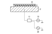
支持テーブル2のほぼ中央には、高周波電力を供給するための給電線12が接続されており、この給電線12には整合器11および高周波電源10が接続されている。高周波電源10からは所定の周波数の高周波電力が支持テーブル2に供給されるようになっている。一方、下部電極として機能する支持テーブル2に対向してその上方には後述するシャワーヘッド16が互いに平行に設けられており、このシャワーヘッド16はチャンバーを介して接地されている。したがって、シャワーヘッド16は上部電極として機能して、支持テーブル2とともに一対の平行平板電極を構成している。
【0027】
これらの電極間距離は40mm以下に設定されることが好ましい。これは、パッシェンの法則(Paschen’s law)より、放電開始電圧Vsは、ガス圧力pと電極間距離dの積pdがある値の時に極小値(パッシェン最小値)をとり、パッシェン最小値をとるpdの値は高周波電力の周波数が大きいほど小さくなることから、本実施形態のように高周波電力の周波数が大きい場合に放電開始電圧Vsを小さくして放電を容易にし、安定させるためには、ガス圧力pが一定であれば電極間距離dを小さくする必要があるからである。また、電極間距離を40mm以下とすることで、チャンバー内でのガスのレジデンスタイムを短くすることができるので反応生成物が効率的に排出され、エッチングストップを低減することができるという効果も得られる。
【0028】
上記シャワーヘッド16は、チャンバー1の天壁部分に嵌め込まれている。このシャワーヘッド16は、シャワーヘッド本体16aと、その下面に交換可能に設けられた電極板18とを有している。シャワーヘッド本体16aの下部および電極板18を貫通するように多数のガス吐出孔17が設けられており、シャワーヘッド本体16aの上部にガス導入部16bを有し、内部には空間16cが形成されている。ガス導入部16bにはガス供給配管15aが接続されており、このガス供給配管15aの他端には、エッチング用の処理ガスを供給する処理ガス供給装置15が接続されている。
【0029】
エッチングのための処理ガスとしては、N2、H2、O2、CO、NH3、CxHy(ただし、x、yは自然数である)で表されるガス等の分子性ガスに、基底状態からの電離エネルギーもしくは準安定状態からの電離エネルギーが10eV以下、かつ最大電離断面積が2×1016cm2以上のガス(以下、電離促進ガスと呼ぶ)を添加したものを用いる。このような電離促進ガスを添加することにより、プラズマ密度(電子密度)を低下させることなく、その分布を大幅に改善することができる。
【0030】
このような電離促進ガスとしては、Ar、Xe、Krが好適である。その中でも特にArが好適である。Arの基底状態からの電離エネルギーは15.8eVであり、N2やH2等の分子性ガスと大差はないが、Arには5秒程度保持可能な準安定状態が基底状態から11.55eV、11.72eVのエネルギーレベルの部分に存在し、その準安定状態からは、約4eVで電離状態に遷移することができる。また、図3に示すように、Arは最大電離断面積が3×1016cm2程度であり、N2やH2等の分子性ガスよりも大きい。したがって、処理ガスにArを添加することにより、処理ガスの電離を著しく促進する。Xe、Krも準安定状態が存在し、比較的低いエネルギーで電離状態に遷移することができ、また、図4に示すようにArよりも最大電離断面積が大きい。同じ希ガスでもHeやNeは図4に示すように最大電離断面積が小さい。また、He、Neは電離エネルギーが大きい。例えばHeでは基底状態からの電離エネルギーが24.6eVである。
【0031】
上記分子性ガスとしては、N2とH2との組み合わせ、NH3、これらとO2との組み合わせ、N2とO2との組み合わせ、CH4またはC2H6とO2との組み合わせ等を挙げることができる。これらの中では、N2とH2との組み合わせ、およびNH3が好ましい。したがって、処理ガスの組み合わせとしては、ArとN2とH2との組み合わせ、ArとNH3との組み合わせが好適である。処理ガス中の分子性ガスに対する電離促進ガスの流量比は0.5以上の範囲が好ましい。
【0032】
このような処理ガスが、処理ガス供給装置15からガス供給配管15a、ガス導入部16bを介してシャワーヘッド本体16a内の空間16cに至り、ガス吐出孔17から吐出され、ウエハWに形成された膜のエッチングに供される。
【0033】
チャンバー1の底壁には、排気管19接続されており、この排気管19には真空ポンプ等を含む排気装置20が接続されている。そして排気装置20の真空ポンプを作動させることによりチャンバー1内を所定の真空度まで減圧することができるようになっている。一方、チャンバー1の側壁上側には、ウエハWの搬入出口23を開閉するゲートバルブ24が設けられている。
【0034】
一方、チャンバー1の搬入出口23の上下にチャンバー1を周回するように、同心状に、2つのリング磁石21a,21bが配置されており、支持テーブル2とシャワーヘッド16との間の処理空間の周囲に磁界を形成するようになっている。このリング磁石21a,21bは、図示しない回転機構により回転可能に設けられている。
【0035】
リング磁石21a,21bは、図2の水平断面図に示すように、永久磁石からなる複数のセグメント磁石22が図示しない支持部材により支持された状態でリング状に配置されて構成されている。この例では、16個のセグメント磁石22がリング状(同心円状)にマルチポール状態で配置されている。すなわち、リング磁石21a,21bにおいては、隣接する複数のセグメント磁石22同士の磁極の向きが互いに逆向きになるように配置されており、したがって、磁力線が図示のように隣接するセグメント磁石22間に形成され、処理空間の周辺部のみに例えば0.02〜0.2T(200〜2000Gauss)、好ましくは0.03〜0.045T(300〜450Gauss)の磁場が形成され、ウエハ配置部分は実質的に無磁場状態となる。このように磁場強度が規定されるのは、磁場が強すぎると洩れ磁場の原因となり、弱すぎるとプラズマ閉じこめ効果が得られなくなるためである。ただし、適正な磁場強度は装置構造等にも依存するため、その範囲は装置によって異なるものである。
【0036】
また、処理空間の周辺部にこのような磁場が形成された場合に、フォーカスリング5上の磁場強度が0.001T(10Gauss)以上となることが望ましい。これにより、フォーカスリング上に電子のドリフト運動(E×Bドリフト)を生じさせてウエハ周辺部のプラズマ密度が上昇してプラズマ密度が均一化される。一方、ウエハWのチャージアップダメージを防止する観点から、ウエハWの存在部分の磁場強度は0.001T(10Gauss)以下となることが望ましい。
【0037】
ウエハ配置部分における実質的に無磁場状態とは、完全に磁場が存在しない場合のみならず、ウエハ配置部分にエッチング処理に影響を与える磁場が形成されず、実質的にウエハ処理に影響を与えない磁場が存在する場合も含む。
【0038】
このようなマルチポール状態のリング磁石によって磁場を形成すると、チャンバー1の壁部の磁極に対応する部分(例えば図2のPで示す部分)が局部的に削られる現象が生じるおそれがあるが、図示しない回転機構によりリング磁石21a,21bをチャンバーの円周方向に沿って回転させることにより、チャンバー壁に対して局部的に磁極が当接することが回避され、チャンバー壁が局部的に削られることが防止される。
【0039】
上記各セグメント磁石22は、図示しないセグメント磁石回転機構により垂直方向の軸を中心に回転自在に構成されている。このようにセグメント磁石22を回転させることにより、実質的にマルチポール磁場が形成される状態とマルチポール磁場が形成されない状態との間で切替可能となっている。条件によってはウエハ処理にマルチポール磁場が有効に作用する場合と、作用しない場合とがあるから、このようにマルチポール磁場を形成した状態と形成しない状態とを切替可能とすることにより、条件に応じて適切なほうを選択することができる。
【0040】
磁場の状態はセグメント磁石の配置に応じて変化するから、セグメント磁石の配置を種々変化させることにより種々の磁場強度プロファイルを形成することができる。したがって、必要な磁場強度プロファイルが得られるように、セグメント磁石を配置することが好ましい。
【0041】
なお、セグメント磁石の数はこの例に限定されるものではない。また、その断面形状もこの例のように長方形に限らず、円、正方形、台形等、任意の形状を採用することができる。セグメント磁石22を構成する磁石材料も特に限定されるものではなく、例えば、希土類系磁石、フェライト系磁石、アルニコ磁石等、公知の磁石材料を適用することができる。
【0042】
プラズマ密度およびイオン引き込み作用を調整するために、プラズマ生成用の高周波電力とプラズマ中のイオンを引き込むための高周波電力とを重畳させてもよい。具体的には、図5に示すように、プラズマ生成用の高周波電源10の他にイオン引き込み用の高周波電源26を整合器11に接続し、これらを重畳させる。この場合に、イオン引き込み用の高周波電源26としては、周波数が500KHz〜27MHzが好ましい。これにより、イオンエネルギーを制御して有機系材料膜のエッチングレートをより上昇させることができる。この場合に、このイオン引き込み用の高周波電源26からの高周波電力の供給は、下部電極としての支持テーブル2の自己バイアス電圧Vdcの絶対値が500V以下になるようにして行う。より好ましくはVdcの絶対値が200V以下である。
【0043】
また、図6に示すように、上部電極であるシャワーヘッド16にプラズマ形成用の高周波電源10′を整合器11′を介して接続し、下部電極である支持テーブル2にイオン引き込み用の高周波電源26のみを整合器11を介して接続するようにしてもよい。この場合には支持テーブル2にバイアスをかけないとエッチングが進行しないため、イオン引き込み用の高周波電源26は必須である。この場合にも、このイオン引き込み用の高周波電源26からの高周波電力の供給は、下部電極としての支持テーブル2の自己バイアス電圧Vdcの絶対値が500V以下になるようにして行う。より好ましくはVdcの絶対値が200V以下である。
【0044】
なお、高周波電源10、整合器11、直流電源13、処理ガス供給装置15、冷媒制御装置8、伝熱ガス供給装置9、排気装置20等は、制御部25により制御される。
【0045】
次に、このように構成されるプラズマエッチング装置によって、無機系材料をマスクとして、有機系材料膜である低誘電率膜(low−k膜)をエッチングする際の処理動作について説明する。
【0046】
エッチング前のウエハWは、図7の(a)に示すように、シリコン基板41の上に層間絶縁層としてlow−k膜である有機系材料膜42が形成され、その上にハードマスクとして所定のパターンの無機系材料膜43が形成され、さらにその上にBARC層44が形成され、その上に所定パターンのレジスト膜45が形成されて構成されている。
【0047】
無機系材料膜43は、一般的なハードマスクとして用いられる材料で構成されており、シリコン酸化物、シリコン窒化物、シリコン酸窒化物を好適な例として挙げることができる。
【0048】
エッチング対象膜である有機系材料膜42は、上述のように層間絶縁膜として用いられるlow−k膜であり、比誘電率が従来の層間絶縁層材料であるシリコン酸化物よりも極めて小さい。このような有機系材料系low−k膜としては、例えば、ビスベンゾシクロブテン樹脂(BCB)やDowChemical社製のSiLK(商品名)やFLARE(商品名)等のポリアリーレンエーテル樹脂(PAE)、メチルシルセスキオキサン(MSQ)等の有機ポリシロキサン樹脂等がある。ここで、有機ポリシロキサンとは、以下に示すように、シリコン酸化膜の結合構造中にC、Hを含む官能基を含む構造を有するものをいう。以下に示す構造中、Rはメチル基、エチル基、プロピル基等のアルキル基もしくはその誘導体、またはフェニル基等のアリール基もしくはその誘導体を示す。
【0049】
【化1】

このような構造のウエハWについては、まず、レジスト膜45をマスクとしてBARC層44および無機系材料膜43をエッチングして図7の(b)に示す構造とする。この際に、レジスト膜45はエッチングにより厚さが減少している。
【0051】
次に、このような構造のウエハWの有機系材料膜42をレジスト膜45および無機系材料膜43をマスクとしてエッチングを行う。この際には、図1の装置のゲートバルブ24を開にして搬送アームにて図7の(b)の構造のウエハWをチャンバー1内に搬入し、支持テーブル2上に載置した後、搬送アームを退避させてゲートバルブ24を閉にし、排気装置20の真空ポンプにより排気管19を介してチャンバー1内を所定の真空度にする。
【0052】
その後、チャンバー1内に処理ガス供給装置15から処理ガスとして、上述したように所定の分子性ガスと電離促進ガスとを所定の流量比で導入する。例えばN2およびH2およびArをそれぞれ180mL/min、180mL/min、360mL/minの流量で導入し、チャンバー1内を所定の圧力、例えば1.33〜133.3Pa(10〜1000mTorr)程度に維持する。このように所定の圧力に保持した状態で高周波電源10から支持テーブル2に、周波数が40MHz以上、例えば100MHzの高周波電力を供給する。このとき、直流電源13から静電チャック6の電極6aに所定の電圧が印加され、ウエハWは例えばクーロン力により吸着される。
【0053】
このようにして下部電極である支持テーブル2に高周波電力が印加されることにより、上部電極であるシャワーヘッド16と下部電極である支持テーブル2との間の処理空間には高周波電界が形成され、これにより処理空間に供給された処理ガスがプラズマ化されて、そのプラズマにより有機系材料膜42がエッチングされる。このエッチングの際に、途中まではレジスト膜45がマスクとして機能するが、エッチング中にレジスト膜45およびBARC層44がエッチングされて消滅し、その後は、無機系材料膜43のみをマスクとして有機系材料膜42のエッチングが続行される。
【0054】
このエッチングの際に、マルチポール状態のリング磁石21a,21bにより、処理空間の周囲に図2に示すような磁場を形成することにより、プラズマ閉じこめ効果が発揮され、本実施形態のようにプラズマの不均一が生じやすい高周波数の場合でも、ウエハWのエッチングレートを均一化することができる。また、膜によってはこのような磁場の効果がない場合もあるが、その場合には、セグメント磁石22を回転させて処理空間の周囲に実質的に磁場を形成しないようにして処理を行えばよい。
【0055】
上記磁場を形成した場合には、支持テーブル2上のウエハWの周囲に設けられた導電性または絶縁性のフォーカスリング5によりプラズマ処理の均一化効果を一層高めることができる。すなわち、フォーカスリング5がシリコンやSiC等の導電性材料で形成されている場合、フォーカスリング領域までが下部電極として機能するため、プラズマ形成領域がフォーカスリング5上まで広がり、ウエハWの周辺部におけるプラズマ処理が促進されエッチングレートの均一性が向上する。またフォーカスリング5が石英等の絶縁性材料の場合、フォーカスリング5とプラズマ中の電子やイオンとの間で電荷の授受を行えないので、プラズマを閉じこめる作用を増大させることができエッチングレートの均一性が向上する。
【0056】
このようなエッチングにおいて、有機系材料のエッチングはプラズマ密度が支配的であってイオンエネルギーの寄与が小さいのに対し、無機系材料のエッチングではプラズマ密度とイオンエネルギーの両方が必要である。したがって、このような無機系材料膜43をマスクとする有機系材料膜42のエッチングにおいては、有機系材料膜42のエッチングレートを低下させずに、無機系材料膜43に対するエッチング選択比を高くしてエッチングするためには、プラズマ密度を低下させずにイオンエネルギーを低くすることが必要である。つまり、有機系材料のエッチングに支配的なプラズマ密度を低下させずに無機系材料のエッチングに必要なイオンエネルギーを低くすれば、Arのような原子ガスが含まれていても有機系材料膜42のみが選択的に高エッチングレートでエッチングされることとなる。ここで、プラズマのイオンエネルギーは、エッチングの際における電極の自己バイアス電圧で間接的に把握することができるから、有機系材料膜42のエッチングレートを低下させずに高エッチング選択比でエッチングするためには、結局、プラズマ密度を低下させずに自己バイアス電圧を低くしてエッチングすることが必要となる。具体的には、プラズマ密度を1×1011cm−3程度に維持しつつ、自己バイアス電圧Vdcの絶対値を500V以下とすることが必要となる。
【0057】
図8は、横軸に自己バイアス電圧Vdcをとり、縦軸にプラズマ密度をとって、高周波電力の周波数が40MHz、100MHzにおけるこれらの関係を示す図であり、プラズマガスとして評価用のArを用いた結果を示すものである。なお、各周波数において、印加する高周波パワーを変化させることによりプラズマ密度Neおよび自己バイアス電圧Vdcの値を変化させた。つまり、各周波数とも印加する高周波パワーが大きくなるほどプラズマ密度Neおよび自己バイアス電圧Vdcがともに大きくなる。また、プラズマ密度は、マイクロ波干渉計により測定した。この図8に示すように、高周波電力の周波数が40MHzの場合に、有機系材料膜を実用的なエッチングレートを実現可能なプラズマ密度1×1011cm−3において自己バイアス電圧Vdcが300Vと低い値を示し、周波数が100MHzの場合には、プラズマ密度1×1011cm−3において自己バイアス電圧Vdcが100V以下とさらに低下する。したがって、プラズマ形成用の高周波電力の周波数を40MHz以上にすれば、有機系材料膜のエッチングに実用的なプラズマ密度1×1011cm−3付近においてVdcが500V以下と無機系材料膜43へのダメージの小さいエッチングを行うことができる。図8に示すように、プラズマ形成用の高周波電力の周波数が上昇するほど、プラズマ密度の上昇にともなう自己バイアス電圧Vdcの絶対値の上昇が小さくなることから、周波数が高くなるほど好ましいが、150MHzを超えるとプラズマの均一性が低下する傾向にあることから150MHz以下であることが好ましい。実用的には100MHz程度であることが好ましい。なお、自己バイアス電圧Vdcの絶対値はより小さいほうが好ましく200V以下であることが好ましい。
【0058】
図5に示すように、プラズマ密度およびイオン引き込み作用を調整するために、プラズマ生成用の高周波電力とプラズマ中のイオンを引き込むための高周波電力とを重畳させることができるが、その場合には、下部電極である支持テーブル2の自己バイアス電圧Vdcの絶対値が500V以下、好ましくは200V以下となるようにその周波数とパワーを調整する。また、図6に示すように上部電極であるシャワーヘッド16にプラズマ形成用の40MHz以上の高周波電力を印加することができ、その場合には下部電極である支持テーブル2へのイオンを引き込むための高周波電力の印加が必須であるが、この際にも下部電極である支持テーブル2の自己バイアス電圧Vdcの絶対値が500V以下、好ましくは200V以下となるようにその周波数とパワーを調整する。
【0059】
このようにプラズマ形成用の高周波電力の周波数が高くなって40MHz以上となれば、自己バイアス電圧の絶対値が500V以下と小さいので、Arのようなエッチング作用の大きい原子ガスを処理ガスとして用いても、そのエネルギーが小さく無機材料膜43をエッチングする能力はあまり高くない。むしろ、Arに代表される電離促進ガス、つまり、低いエネルギーで電離し、最大電離断面積が大きいガスを用いることにより電子密度すなわちプラズマ密度を均一化することが可能となる。本実施形態では、上述したように、Ar、Xe、Krに代表される基底状態からの電離エネルギーもしくは準安定状態からの電離エネルギーが10eV以下、かつ最大電離断面積が2×1016cm2以上の電離促進ガスを添加するため、処理ガスが電離しやすいものとなり、電界強度が低い被処理体の端部近傍部分においても処理ガスを十分に電離させることができ、全体的に均一に電離される結果、電子密度すなわちプラズマ密度が均一となる。
【0060】
このことを確認した実験結果について説明する。
図9の(a)、(b)は各ガスのプラズマ密度(電子密度)の均一性を示す図である。ここでは、チャンバー内圧力を4Pa、ウエハ周辺の磁場を0.003T(30Guss)にして、下部電極に100MHzで2400Wおよび1200Wの高周波電力を印加して、300mmウエハの径方向の位置とプラズマ密度の関係を求めた。図9から、H2、N2、O2の分子性ガスやHeではプラズマ密度の均一性が極めて悪いのに対し、電離促進ガスであるArはほぼ均一であることがわかる。
【0061】
図10は、処理ガスとして通常用いられるN2/H2を用いた場合の300mmウエハの径方向の位置とプラズマ密度(電子密度)との関係を示す図である。ここでは、チャンバー内圧力を4Pa、ウエハ周辺磁場を0.03T(300Guss)とし、N2流量:180mL/min、H2流量:180mL/minとして、下部電極に100MHzで600W、1200W、2400Wの高周波電力を印加した。この図から、N2/H2ではいずれのパワーでも中心部のプラズマ密度が高く不均一な分布となることがわかる。
【0062】
図11は、処理ガスとしてN2/H2を用いた場合、およびさらにArを添加した場合の300mmウエハの径方向の位置とプラズマ密度の関係を示す図である。ここでは、チャンバー内圧力を4Pa、ウエハ周辺磁場を0.03T(300Guss)とし、N2流量:180mL/min、H2流量:180mL/minでAr流量を0、200、400mL/minと変化させ、下部電極に100MHzで2400Wの高周波電力を印加した。この図から、N2/H2にArを添加することにより、プラズマ密度の均一性が大幅に改善されることがわかる。
【0063】
図12は、処理ガスとして通常用いられるNH3を用いた場合、およびさらにArを添加した場合の300mmウエハの径方向の位置とプラズマ密度の関係を示す図である。ここでは、チャンバー内圧力を4Pa、ウエハ周辺磁場を0.03T(300Guss)とし、NH3流量:240mL/minでAr流量を0、240mL/minと変化させ、下部電極に100MHzで2400Wの高周波電力を印加した。この図から、NH3にArを添加することにより、プラズマ密度の均一性が大幅に改善されることがわかる。
【0064】
次に、実際に無機系材料膜をマスクとして有機材料膜をエッチングした場合について説明する。
ここでは、300mmウエハで、有機材料膜としてDowChemical社製のSiLK(商品名)を用い、無機系材料膜としてSiO2を用いた場合について、チャンバー内圧力を4Pa、ウエハ周辺磁場を0.03T(300Guss)とし、N2流量:180mL/min、H2流量:180mL/minをベースとし、Ar流量:0、360、720mL/minと変化させ、下部電極に100MHzで2400Wの高周波電力を印加してエッチングを行った。図13は、この際のウエハ径方向の有機系材料膜および無機系材料膜のエッチングレートを示す図である。なお、ウエハの径方向としては直交する2方向(x方向、y方向)を用いた。この図から、Arを添加することにより、エッチングレートの均一性も向上することがわかる。
【0065】
図14は、上記エッチング実験について、横軸にAr流量をとり、縦軸にウエハ径方向のエッチング均一性および平均エッチングレートをとってこれらの関係を示す図である。この図に示すように、Ar添加により、エッチングレートを低下させずにエッチングレートの均一性が向上することが確認された。また、Ar流量が増加するほど均一性が良好になることが確認された。
【0066】
図15は、上記エッチング実験について、Ar流量とSiLKのSiO2に対するエッチング選択比(SiLK/SiO2;以下、単にエッチング選択比と記す)との関係を示すものであり、(a)はAr流量が0mL/min、360mL/min、720mL/minの場合におけるウエハ径方向の位置に対するエッチング選択比を示すもの、(b)はAr流量とエッチング選択比との関係をセンターとエッジ5mmの位置で示すものである。この図に示すように、Ar添加によりエッチング選択比の低下は見られず、むしろAr添加により選択比は向上し、マスクの肩落ちが減少する方向に作用することが確認された。
【0067】
なお、本発明は上記実施の形態に限定されることなく種々変更可能である。例えば、上記実施形態では、磁場形成手段として永久磁石からなる複数のセグメント磁石をチャンバーの周囲にリング状に配置してなるマルチポール状態のリング磁石を用いたが、処理空間の周囲に磁場を形成してプラズマを閉じこめることができればこれに限定されるものではない。また、このようなプラズマ閉じこめ用の周辺磁場は必ずしも必要ではなく、磁場が存在しない状態でエッチングを行ってもよい。また、処理空間に水平磁場を印加して直交電磁界中でプラズマエッチングを行うプラズマエッチング処理であってもよい。さらに、上記実施形態では有機系材料膜としてlow−k膜を用いたが、これに限定されることなく、多層レジストに用いられる有機系材料膜等の他の膜も適用可能である。さらにまた、電離促進ガスとしてArを中心に説明し、他にXe、Krを例示したが、基底状態からの電離エネルギーもしくは準安定状態からの電離エネルギーが10eV以下、かつ最大電離断面積が2×1016cm2以上のガスであればこれらに限るものではない。さらにまた、上記実施形態では無機系材料膜をマスクとして有機系材料膜をエッチングした場合について示したが、本発明は、これに限らず、無機系材料膜に対して選択的に有機系材料膜をエッチングする必要がある場合全てに適用可能である。例えば、Siウエハ等の被処理基板上に形成されたSiO2等の無機材料膜をエッチングする際のマスクとして用いられたレジストを除去するアッシングに本発明を適用することが可能である。つまり、アッシングは下地の無機系材料膜を極力エッチングすることなく、有機系材料膜であるレジスト膜を選択的に効率良く除去する必要があることから、本発明をアッシングに適用することにより、良好なアッシング特性を得ることができる。さらにまた、上記実施形態では被処理基板として半導体ウエハを用いた場合について示したが、これに限らず他の基板のプラズマ処理にも適用することができる。
【0068】
【発明の効果】
以上説明したように、本発明によれば、プラズマ形成用として電極に印加する高周波電力の周波数を40MHz以上と従来よりも高くすることにより、有機系材料膜のエッチングに必要なプラズマ密度を確保しつつ低い自己バイアス電圧を実現することができ、有機系材料膜を無機系材料膜に対して高エッチング選択比でエッチングすることができるとともに、Ar、Xe、Krに代表される基底状態からの電離エネルギーもしくは準安定状態からの電離エネルギーが10eV以下、かつ最大電離断面積が2×1016cm2以上のガスを含む処理ガスを用いることにより、プラズマ密度(電子密度)を低下させることなく、その分布を大幅に改善することができる。
【図面の簡単な説明】
【図1】本発明の実施に用いられるプラズマエッチング装置の一例を示す断面図。
【図2】図1の装置のチャンバーの周囲に配置されたリング磁石を模式的に示す水平断面図。
【図3】各ガスの電子エネルギーと電離断面積との関係を示す図。
【図4】希ガスの電子エネルギーと電離断面積との関係を示す図。
【図5】プラズマ生成用の高周波電源とイオン引き込み用の高周波電源を下部電極である支持テーブルに接続したプラズマ処理装置を部分的に示す概略断面図。
【図6】プラズマ生成用の高周波電源を上部電極であるシャワーヘッドに接続し、イオン引き込み用の高周波電源を下部電極である支持テーブルに接続したプラズマ処理装置を部分的に示す概略断面図。
【図7】本発明のプラズマエッチングが適用されるウエハの構造例を示す断面図。
【図8】アルゴンガスのプラズマにおいて、高周波電力の周波数が40MHz、100MHzにおける自己バイアス電圧Vdcとプラズマ密度Neとの関係を示す図。
【図9】各ガスのプラズマ密度(電子密度)の均一性を示す図。
【図10】処理ガスとして通常用いられるN2/H2を用いた場合の300mmウエハの径方向の位置とプラズマ密度(電子密度)との関係を示す図。
【図11】処理ガスとしてN2/H2を用いた場合、およびさらにArを添加した場合の300mmウエハの径方向の位置とプラズマ密度の関係を示す図。
【図12】処理ガスとして通常用いられるNH3を用いた場合、およびさらにArを添加した場合の300mmウエハの径方向の位置とプラズマ密度の関係を示す図。
【図13】実際に無機系材料膜をマスクとして有機材料膜をエッチングした際の処理ガス中のArガスの流量とウエハ径方向の有機系材料膜および無機系材料膜のエッチングレートとの関係を示す図。
【図14】Ar流量とウエハ径方向のエッチング均一性との関係およびAr流量と平均エッチングレートとの関係を示す図。
【図15】Ar流量とSiLKのSiO2に対するエッチング選択比との関係を示す図。
【符号の説明】
1;チャンバー
2;支持テーブル(電極)
5;フォーカスリング
10,26;高周波電源
15;処理ガス供給装置
16;シャワーヘッド(電極)
20;排気装置
21a,21b;リング磁石(磁場形成手段)
22;セグメント磁石
W;半導体ウエハ(被処理基板)[0001]
TECHNICAL FIELD OF THE INVENTION
The present invention relates to a plasma etching method for performing plasma etching of an organic material film on a substrate such as a semiconductor wafer on which an organic material film such as a low dielectric constant film (low-k film) is formed.
[0002]
[Prior art]
In a wiring step of a semiconductor device, an interlayer insulating film is formed between wiring layers, and the interlayer insulating film is etched to make the wiring layers conductive. In recent years, as the interlayer insulating film, a film having a lower dielectric constant has been demanded due to a demand for higher speed of a semiconductor device, and an organic material film has been used as such a low dielectric constant film. .
[0003]
Etching of such an organic material film is performed by plasma etching using an inorganic material film such as silicon oxide as a mask. Specifically, a semiconductor wafer (hereinafter simply referred to as a wafer) is placed on a lower electrode by using a parallel plate type plasma etching apparatus provided with a pair of opposed electrodes vertically opposed in a chamber. A high frequency power having a frequency of 13.56 MHz is supplied to the electrode, and N is used as a processing gas. 2 , H 2 , Ar and the like are used (
[0004]
[Patent Document 1]
JP-A-2001-60582 (Claims, paragraphs 0022 to 0024, etc.)
[Patent Document 2]
JP 2001-118825 A (Claims, paragraphs 0015, 0022, etc.)
[0005]
[Problems to be solved by the invention]
However, when the organic material film is etched under the conventional etching conditions as described in
[0006]
Further, in order to prevent such a shoulder drop and to etch the organic material film with a high selectivity, a molecular single gas other than an atomic gas such as Ar gas having a strong etching action (strong sputtering action) is used. Alternatively, when a mixed gas is used, the electron density (plasma density) becomes extremely poor in uniformity such as high in the center and low in the edges corresponding to the electric field intensity distribution. Therefore, the uniformity of the obtained etching must be poor. In particular, when the diameter of the wafer is increased to 300 mm, the non-uniformity of the electron density (plasma density) becomes more remarkable.
[0007]
The present invention has been made in view of such circumstances, and when etching an organic material film, has high selectivity to an adjacent inorganic material film, and increases the uniformity of electron density or plasma density. It is an object of the present invention to provide a plasma etching method capable of performing etching by etching and a plasma etching apparatus realizing the method.
[0008]
[Means for Solving the Problems]
According to the study results of the present inventors, etching of an organic material film is dominated by plasma density and the contribution of ion energy is small, whereas etching of an inorganic material film has both plasma density and ion energy. Therefore, in order to increase the etching selectivity to the inorganic material film without lowering the etching rate of the organic material film, it is necessary to lower the ion energy without lowering the plasma density. Was found. In this case, since the ion energy of the plasma can be indirectly grasped by the self-bias voltage of the electrode at the time of etching, the organic material film is etched at a high etching selectivity without lowering the etching rate. After all, it is necessary to perform etching under low bias conditions without lowering the plasma density. According to the results of further studies by the present inventors, it has been found that when the frequency of the high-frequency power applied to the electrode increases, a state in which the self-bias voltage is small can be formed without lowering the plasma density.
[0009]
Also, when the frequency of the high frequency power for plasma formation is increased to 40 MHz or more, the self-bias voltage is small, so that even if an atomic gas such as Ar is used as a processing gas, the ability to etch the inorganic material film can be obtained. It has been found that the electron density, that is, the plasma density can be made uniform by using a gas that ionizes with low energy, such as Ar, or a gas having a large ionization cross section, such as Ar.
[0010]
That is, according to a first aspect of the present invention, there is provided a plasma etching method for plasma-etching an organic material film on an object to be processed using a parallel plate type plasma etching apparatus, wherein high-frequency power for forming plasma is provided. The frequency is 40 MHz or more, the ionization energy from the ground state or the ionization energy from the metastable state is 10 eV or less, and the maximum ionization cross section is 2 × 10 16 cm 2 A plasma etching method is characterized in that the organic material film is plasma-etched using a processing gas containing the above gases.
[0011]
According to a second aspect of the present invention, there is provided a plasma etching method for plasma etching an organic material film on an object to be processed by using a parallel plate type plasma etching apparatus, wherein a pair of parallel plate electrodes disposed in a chamber are provided. Applying a high frequency power of 40 MHz or more for forming plasma to the electrode supporting the object to be processed in a state where the object is supported on one side, and ionizing energy from the ground state or ionizing from the metastable state Energy of 10 eV or less and maximum ionization cross section of 2 × 10 16 cm 2 A plasma etching method is characterized in that the organic material film is plasma-etched using a processing gas containing the above gases.
[0012]
According to a third aspect of the present invention, there is provided a plasma etching method for plasma etching an organic material film on an object to be processed using a parallel plate type plasma etching apparatus, wherein a pair of parallel plate electrodes arranged in a chamber are provided. With the object to be processed supported on one side, high-frequency power of 40 MHz or more for forming plasma is applied to the electrode supporting the object to be processed, and the absolute value of the self-bias voltage is further applied to the electrode. A high frequency power of 500 kHz to 27 MHz for ion attraction is superimposed and applied so as to be 500 V or less, ionization energy from the ground state or ionization energy from the metastable state is 10 eV or less, and the maximum ionization cross section is 2 × 10 16 cm 2 A plasma etching method is characterized in that the organic material film is plasma-etched using a processing gas containing the above gases.
[0013]
According to a fourth aspect of the present invention, there is provided a plasma etching method for plasma etching an organic material film on an object to be processed using a parallel plate type plasma etching apparatus, wherein a pair of parallel plate electrodes arranged in a chamber is provided. Applying high-frequency power of 40 MHz or more for forming plasma to the other electrode in a state where the object to be processed is supported on one of the electrodes, and the absolute value of the self-bias voltage of the electrode supporting the object to be processed is 500 V or less A high frequency power of 500 kHz to 27 MHz for ion attraction is applied so that the ionization energy from the ground state or the ionization energy from the metastable state is 10 eV or less and the maximum ionization cross section is 2 × 10 16 cm 2 A plasma etching method is characterized in that the organic material film is plasma-etched using a processing gas containing the above gases.
[0014]
According to a fifth aspect of the present invention, there is provided a plasma etching apparatus for plasma-etching an organic material film on a substrate to be processed, wherein the chamber is provided in the chamber for accommodating the substrate to be processed, and one of the chambers is provided in one of the chambers. A pair of parallel plate electrodes on which a processing substrate is supported, a processing gas supply system for supplying a processing gas into the chamber, an exhaust system for exhausting the chamber, and formation of plasma on the electrode on which the substrate to be processed is supported A high-frequency power supply for supplying high-frequency power for use, the frequency of the high-frequency power supplied from the high-frequency power supply is 40 MHz or more, the processing gas supply system, ionization energy from the ground state or from the metastable state The ionization energy is 10 eV or less and the maximum ionization cross section is 2 × 10 16 cm 2 A plasma etching apparatus characterized by supplying a processing gas containing the above gases is provided.
[0015]
According to a sixth aspect of the present invention, there is provided a plasma etching apparatus for plasma-etching an organic material film on a substrate to be processed, wherein the chamber is provided in the chamber for accommodating the substrate to be processed, and one of the chambers is provided in one of the chambers. A pair of parallel plate electrodes on which a processing substrate is supported, a processing gas supply system for supplying a processing gas into the chamber, an exhaust system for exhausting the chamber, and formation of plasma on the electrode on which the substrate to be processed is supported A first high-frequency power supply for supplying high-frequency power for use with the substrate, and a second high-frequency power supply for supplying high-frequency power for ion attraction superimposed on the electrode on which the substrate to be processed is supported, The frequency of the high-frequency power supplied from the high-frequency power supply to the electrode supporting the substrate to be processed is 40 MHz or more, and the substrate to be processed is supported from the second high-frequency power supply. The high frequency power supplied to the electrode to be applied is applied so that the frequency is in the range of 500 kHz to 27 MHz and the absolute value of the self-bias voltage of the electrode is 500 V or less. Has an ionization energy of 10 eV or less from the metastable state and a maximum ionization cross section of 2 × 10 16 cm 2 A plasma etching apparatus characterized by supplying a processing gas containing the above gases is provided.
[0016]
According to a seventh aspect of the present invention, there is provided a plasma etching apparatus for plasma-etching an organic material film of a substrate to be processed, wherein the chamber is provided in the chamber for accommodating the substrate to be processed, and one of the chambers is provided in the chamber. A pair of parallel plate electrodes on which a processing substrate is supported, a processing gas supply system for supplying a processing gas into the chamber, an exhaust system for exhausting the inside of the chamber, and a substrate to be processed among the pair of parallel plate electrodes A first high-frequency power supply for supplying high-frequency power for plasma formation to an unsupported electrode, and a second high-frequency power supply for supplying high-frequency power for ion attraction to the electrode on which the substrate to be processed is supported, The frequency of the high frequency power supplied from the first high frequency power supply to the electrode on which the substrate to be processed is not supported is 40 MHz or more, and the frequency of the second high frequency power supply is The high-frequency power supplied to the electrode supporting the substrate to be processed is applied so that the frequency is in the range of 500 kHz to 27 MHz and the absolute value of the self-bias voltage of the electrode is 500 V or less. The system has an ionization energy from the ground state or an ionization energy from the metastable state of 10 eV or less and a maximum ionization cross section of 2 × 10 16 cm 2 A plasma etching apparatus characterized by supplying a processing gas containing the above gases is provided.
[0017]
According to the first aspect of the present invention, by increasing the frequency of the high-frequency power applied to the electrode for plasma formation to 40 MHz or higher, which is higher than the conventional frequency, it is possible to secure the plasma density required for etching the organic material film. A low self-bias voltage can be realized, an organic material film can be etched with a high etching selectivity with respect to an inorganic material film, and ionization energy from a ground state represented by Ar, Xe, and Kr can be obtained. Alternatively, the ionization energy from the metastable state is 10 eV or less and the maximum ionization cross section is 2 × 10 16 cm 2 By using a processing gas containing the above gases, the distribution can be significantly improved without lowering the plasma density (electron density). That is, the ionization energy from the ground state or the ionization energy from the metastable state is 10 eV or less, and the maximum ionization cross section is 2 × 10 16 cm 2 Since the above gases are easily ionized, the addition thereof promotes the ionization of the processing gas. As a result, the processing gas can be sufficiently ionized even in the vicinity of the end of the object to be processed having a low electric field intensity. As a result, the electron density, that is, the plasma density becomes uniform.
[0018]
Specifically, as in the second and fifth aspects of the present invention, the self-bias voltage is reduced by applying high-frequency power of 40 MHz or more for forming plasma to the electrode supporting the object to be processed. Etching with less damage to the inorganic material film can be performed in a low state. Further, as in the third and sixth aspects, if the absolute value of the self-bias voltage of the electrode supporting the object to be processed is in a range of 500 V or less, the electrode supporting the object to be processed may have a frequency of 500 kHz to 27 MHz. By applying high-frequency power in the range, ions can be drawn in a range in which damage to the inorganic material film is small, and the etching property can be improved. Further, as in the fourth and seventh aspects, when high-frequency power of 40 MHz or more for forming plasma is applied to an electrode opposed to the electrode supporting the object, ions are applied to the object. It is necessary to apply high-frequency power in the range of 500 kHz to 27 MHz to the electrode supporting the object to be drawn in, and in this case, the object was supported to reduce damage to the inorganic material film. The absolute value of the self-bias voltage of the electrode is set to 500 V or less.
[0019]
The ionization energy from the ground state or the ionization energy from the metastable state is 10 eV or less, and the maximum ionization cross section is 2 × 10 16 cm 2 It is preferable to use any of Ar, Xe, and Kr as the above gas. In particular, Ar is most effective because it has a metastable state, can transition to an ionized state at about 4 eV therefrom, has a large maximum ionization cross section, and is inexpensive among these. Xe and Kr also have a metastable state, from which they can transition to an ionized state with relatively low energy, and have a large maximum ionized cross section. Specific components of the processing gas include Ar and N 2 And H 2 And further having Ar and NH 3 Can be used.
[0020]
The frequency of the high frequency power for forming the plasma may be 40 MHz or more, but 100 MHz can be suitably used.
[0021]
The distance between the pair of parallel plate electrodes is preferably 40 mm or less. This is for the following reason. According to Paschen's law, the discharge starting voltage Vs takes a minimum value (Paschen minimum value) when the product pd of the gas pressure p and the inter-electrode distance d has a certain value, and the discharge starting voltage Vs takes a Paschen minimum value. Since the value decreases as the frequency of the high-frequency power increases, the discharge pressure Vs is reduced when the frequency of the high-frequency power is high as in the present invention. If the distance is constant, it is necessary to reduce the distance d between the electrodes. Therefore, in the present invention, the distance d between the electrodes is preferably set to 40 mm or less. Further, by setting the distance between the electrodes to 40 mm or less, the residence time of the gas in the chamber can be shortened, so that the reaction product can be efficiently discharged and the etching stop can be reduced. Can be
[0022]
BEST MODE FOR CARRYING OUT THE INVENTION
Hereinafter, embodiments of the present invention will be described with reference to the accompanying drawings.
FIG. 1 is a sectional view showing a plasma etching apparatus used for carrying out the present invention. This etching apparatus has a
[0023]
In the
[0024]
An
[0025]
A
[0026]
A
[0027]
The distance between these electrodes is preferably set to 40 mm or less. According to Paschen's law, the discharge starting voltage Vs takes a minimum value (Paschen minimum value) when the product pd of the gas pressure p and the distance d between the electrodes is a certain value, and the Paschen minimum value is obtained. Since the value of pd decreases as the frequency of the high-frequency power increases, the discharge starting voltage Vs is reduced when the frequency of the high-frequency power is high as in the present embodiment to facilitate discharge and stabilize. This is because if the gas pressure p is constant, it is necessary to reduce the distance d between the electrodes. Further, by setting the distance between the electrodes to 40 mm or less, the residence time of the gas in the chamber can be shortened, so that the reaction products can be efficiently discharged, and the etching stop can be reduced. Can be
[0028]
The
[0029]
The processing gas for etching is N 2 , H 2 , O 2 , CO, NH 3 , C x H y (Where x and y are natural numbers), the ionization energy from the ground state or the ionization energy from the metastable state is 10 eV or less and the maximum ionization cross section is 2 × 10 16 cm 2 A gas to which the above gas (hereinafter, referred to as an ionization promoting gas) is added is used. By adding such an ionization promoting gas, the distribution can be significantly improved without lowering the plasma density (electron density).
[0030]
Ar, Xe, and Kr are preferable as such an ionization promoting gas. Among them, Ar is particularly preferable. The ionization energy of Ar from the ground state is 15.8 eV, and N 2 And H 2 Although there is not much difference from molecular gases such as Ar, a metastable state that can be held for about 5 seconds exists in Ar at an energy level of 11.55 eV and 11.72 eV from the ground state. From the metastable state, It can transition to the ionization state at about 4 eV. As shown in FIG. 3, Ar has a maximum ionization cross-sectional area of 3 × 10 16 cm 2 Degree, N 2 And H 2 Larger than molecular gas such as Therefore, ionization of the processing gas is remarkably promoted by adding Ar to the processing gas. Xe and Kr also have a metastable state, can transition to an ionized state with relatively low energy, and have a larger maximum ionized cross-sectional area than Ar as shown in FIG. Even with the same rare gas, He and Ne have a small maximum ionization cross-sectional area as shown in FIG. He and Ne have a large ionization energy. For example, in He, the ionization energy from the ground state is 24.6 eV.
[0031]
Examples of the molecular gas include N 2 And H 2 In combination with NH 3 , These and O 2 In combination with N 2 And O 2 In combination with CH 4 Or C 2 H 6 And O 2 And the like. Of these, N 2 And H 2 And NH and 3 Is preferred. Therefore, as a combination of the processing gas, Ar and N 2 And H 2 , Ar and NH 3 Is preferable. The flow ratio of the ionization promoting gas to the molecular gas in the processing gas is preferably in the range of 0.5 or more.
[0032]
Such a processing gas reaches the
[0033]
An
[0034]
On the other hand, two
[0035]
As shown in the horizontal cross-sectional view of FIG. 2, the
[0036]
Further, when such a magnetic field is formed in the peripheral portion of the processing space, it is desirable that the magnetic field intensity on the
[0037]
Substantially no magnetic field in the wafer arrangement portion means that not only a magnetic field is completely absent, but also a magnetic field affecting the etching process is not formed in the wafer arrangement portion and does not substantially affect the wafer processing This includes the case where a magnetic field is present.
[0038]
When a magnetic field is formed by such a ring magnet in a multi-pole state, there is a possibility that a portion (for example, a portion indicated by P in FIG. 2) corresponding to the magnetic pole on the wall of the
[0039]
Each of the
[0040]
Since the state of the magnetic field changes according to the arrangement of the segment magnets, various magnetic field intensity profiles can be formed by variously changing the arrangement of the segment magnets. Therefore, it is preferable to arrange the segment magnets so as to obtain a required magnetic field strength profile.
[0041]
Note that the number of segment magnets is not limited to this example. Also, the cross-sectional shape is not limited to a rectangle as in this example, but may be any shape such as a circle, a square, a trapezoid, and the like. The magnet material that constitutes the
[0042]
In order to adjust the plasma density and the ion attracting action, the high frequency power for generating plasma and the high frequency power for attracting ions in the plasma may be superimposed. More specifically, as shown in FIG. 5, a high-
[0043]
As shown in FIG. 6, a high-frequency power source 10 'for plasma formation is connected to a
[0044]
The
[0045]
Next, a description will be given of a processing operation when the low dielectric constant film (low-k film), which is an organic material film, is etched by the plasma etching apparatus having the above-described configuration using an inorganic material as a mask.
[0046]
As shown in FIG. 7A, the wafer W before etching has an
[0047]
The
[0048]
The
[0049]
Embedded image
With respect to the wafer W having such a structure, first, the
[0051]
Next, the
[0052]
Thereafter, as described above, a predetermined molecular gas and an ionization promoting gas are introduced into the
[0053]
By applying the high-frequency power to the support table 2 serving as the lower electrode in this way, a high-frequency electric field is formed in the processing space between the
[0054]
At the time of this etching, by forming a magnetic field as shown in FIG. 2 around the processing space by the
[0055]
When the magnetic field is formed, the uniformity of the plasma processing can be further enhanced by the conductive or insulating
[0056]
In such etching, etching of an organic material is dominated by plasma density and the contribution of ion energy is small, whereas etching of an inorganic material requires both plasma density and ion energy. Therefore, in the etching of the
[0057]
FIG. 8 is a diagram showing the relationship between the self-bias voltage Vdc on the horizontal axis and the plasma density on the vertical axis, where the frequency of the high-frequency power is 40 MHz and 100 MHz, and Ar for evaluation is used as the plasma gas. FIG. At each frequency, the values of the plasma density Ne and the self-bias voltage Vdc were changed by changing the applied high-frequency power. That is, as the high frequency power applied at each frequency increases, both the plasma density Ne and the self-bias voltage Vdc increase. The plasma density was measured with a microwave interferometer. As shown in FIG. 8, when the frequency of the high-frequency power is 40 MHz, the plasma density of the organic material film can be reduced to 1 × 10 4 at which a practical etching rate can be realized. 11 cm -3 , The self-bias voltage Vdc shows a low value of 300 V, and when the frequency is 100 MHz, the plasma density is 1 × 10 11 cm -3 , The self-bias voltage Vdc further decreases to 100 V or less. Therefore, if the frequency of the high frequency power for plasma formation is set to 40 MHz or more, a plasma density of 1 × 10 5 which is practical for etching the organic material film is used. 11 cm -3 In the vicinity, when Vdc is 500 V or less, etching with little damage to the
[0058]
As shown in FIG. 5, in order to adjust the plasma density and the ion attracting action, the high frequency power for plasma generation and the high frequency power for attracting ions in the plasma can be superimposed. The frequency and the power are adjusted so that the absolute value of the self-bias voltage Vdc of the support table 2 as the lower electrode is 500 V or less, preferably 200 V or less. Further, as shown in FIG. 6, high frequency power of 40 MHz or more for plasma formation can be applied to the
[0059]
When the frequency of the high-frequency power for plasma formation is increased to 40 MHz or more, the absolute value of the self-bias voltage is as small as 500 V or less. Therefore, an atomic gas having a large etching effect such as Ar is used as the processing gas. However, its energy is small and its ability to etch the
[0060]
Experimental results confirming this will be described.
FIGS. 9A and 9B are diagrams showing the uniformity of the plasma density (electron density) of each gas. Here, the chamber pressure is set to 4 Pa, the magnetic field around the wafer is set to 0.003 T (30 Guss), high-frequency power of 2400 W and 1200 W is applied to the lower electrode at 100 MHz, and the radial position of the 300 mm wafer and the plasma density are adjusted. Seeking a relationship. From FIG. 9, H 2 , N 2 , O 2 It can be seen that the uniformity of the plasma density is extremely poor in the case of molecular gas or He, whereas Ar, which is an ionization promoting gas, is almost uniform.
[0061]
FIG. 10 shows N which is commonly used as a processing gas. 2 / H 2 FIG. 6 is a diagram showing a relationship between a radial position of a 300 mm wafer and a plasma density (electron density) when using the method shown in FIG. Here, the pressure in the chamber is 4 Pa, the magnetic field around the wafer is 0.03 T (300 Guss), and N 2 Flow rate: 180 mL / min, H 2 At a flow rate of 180 mL / min, high-frequency power of 600 W, 1200 W, and 2400 W at 100 MHz was applied to the lower electrode. From this figure, N 2 / H 2 It can be seen that the plasma density at the center is high and the distribution is non-uniform at any power.
[0062]
FIG. 11 shows that N 2 / H 2 FIG. 6 is a diagram showing the relationship between the radial position of a 300 mm wafer and the plasma density when Ar is used and when Ar is further added. Here, the pressure in the chamber is 4 Pa, the magnetic field around the wafer is 0.03 T (300 Guss), and N 2 Flow rate: 180 mL / min, H 2 At a flow rate of 180 mL / min, the Ar flow rate was changed to 0, 200, and 400 mL / min, and a high frequency power of 2400 W at 100 MHz was applied to the lower electrode. From this figure, N 2 / H 2 It can be seen that the addition of Ar to the substrate significantly improves the uniformity of the plasma density.
[0063]
FIG. 12 shows NH which is usually used as a processing gas. 3 FIG. 6 is a diagram showing the relationship between the radial position of a 300 mm wafer and the plasma density when Ar is used and when Ar is further added. Here, the pressure in the chamber is 4 Pa, the magnetic field around the wafer is 0.03 T (300 Guss), 3 At a flow rate of 240 mL / min, the Ar flow rate was changed to 0 and 240 mL / min, and a high frequency power of 2400 W at 100 MHz was applied to the lower electrode. From this figure, NH 3 It can be seen that the addition of Ar to the substrate significantly improves the uniformity of the plasma density.
[0064]
Next, a case where the organic material film is actually etched using the inorganic material film as a mask will be described.
Here, a 300 mm wafer, SiLK (trade name) manufactured by Dow Chemical Company was used as an organic material film, and
[0065]
FIG. 14 is a diagram showing the relationship between the above-mentioned etching experiments, where the horizontal axis represents the Ar flow rate, and the vertical axis represents the etching uniformity and the average etching rate in the wafer radial direction. As shown in this figure, it was confirmed that the addition of Ar improves the uniformity of the etching rate without lowering the etching rate. It was also confirmed that the higher the Ar flow rate, the better the uniformity.
[0066]
FIG. 15 shows the Ar flow rate and the SiLK SiO 2 Selectivity to Si (SiLK / SiO 2 (Hereinafter simply referred to as an etching selectivity), and (a) shows the etching selectivity with respect to the position in the wafer radial direction when the Ar flow rate is 0 mL / min, 360 mL / min, and 720 mL / min. FIG. 6B shows the relationship between the Ar flow rate and the etching selectivity at the center and the position of the
[0067]
The present invention can be variously modified without being limited to the above embodiment. For example, in the above-described embodiment, a multipole ring magnet in which a plurality of segment magnets made of permanent magnets are arranged in a ring around the chamber is used as the magnetic field forming means, but a magnetic field is formed around the processing space. However, the present invention is not limited to this as long as the plasma can be confined. Further, such a peripheral magnetic field for confining the plasma is not always necessary, and the etching may be performed in the absence of the magnetic field. Alternatively, a plasma etching process in which a horizontal magnetic field is applied to the processing space to perform plasma etching in an orthogonal electromagnetic field may be used. Further, in the above embodiment, the low-k film is used as the organic material film. However, the present invention is not limited to this, and another film such as an organic material film used for a multilayer resist can be applied. Furthermore, Ar has been mainly described as the ionization promoting gas, and Xe and Kr have been exemplified. However, the ionization energy from the ground state or the ionization energy from the metastable state is 10 eV or less, and the maximum ionization cross section is 2 ×. 10 16 cm 2 The above gases are not limited to these. Furthermore, in the above embodiment, the case where the organic material film is etched using the inorganic material film as a mask has been described. However, the present invention is not limited to this, and the organic material film is selectively formed with respect to the inorganic material film. Can be applied to all cases where it is necessary to etch. For example,
[0068]
【The invention's effect】
As described above, according to the present invention, the frequency of the high-frequency power applied to the electrode for forming the plasma is increased to 40 MHz or higher, which is higher than the conventional frequency, thereby securing the plasma density required for etching the organic material film. Low self-bias voltage can be realized while the organic material film can be etched with a high etching selectivity with respect to the inorganic material film, and ionization from the ground state represented by Ar, Xe, and Kr can be achieved. Energy or ionization energy from the metastable state is 10 eV or less and maximum ionization cross section is 2 × 10 16 cm 2 By using a processing gas containing the above gases, the distribution can be significantly improved without lowering the plasma density (electron density).
[Brief description of the drawings]
FIG. 1 is a sectional view showing an example of a plasma etching apparatus used for carrying out the present invention.
FIG. 2 is a horizontal cross-sectional view schematically showing a ring magnet arranged around a chamber of the apparatus of FIG.
FIG. 3 is a diagram showing the relationship between the electron energy of each gas and the ionization cross section.
FIG. 4 is a diagram showing a relationship between electron energy of a rare gas and ionization cross section.
FIG. 5 is a schematic cross-sectional view partially showing a plasma processing apparatus in which a high-frequency power supply for generating plasma and a high-frequency power supply for attracting ions are connected to a support table serving as a lower electrode.
FIG. 6 is a schematic cross-sectional view partially showing a plasma processing apparatus in which a high-frequency power supply for plasma generation is connected to a shower head as an upper electrode, and a high-frequency power supply for ion attraction is connected to a support table as a lower electrode.
FIG. 7 is a cross-sectional view showing a structural example of a wafer to which the plasma etching of the present invention is applied.
FIG. 8 is a diagram showing the relationship between the self-bias voltage Vdc and the plasma density Ne when the frequency of the high-frequency power is 40 MHz and 100 MHz in the argon gas plasma.
FIG. 9 is a diagram showing the uniformity of the plasma density (electron density) of each gas.
FIG. 10: N commonly used as a processing gas 2 / H 2 FIG. 6 is a diagram showing a relationship between a radial position of a 300 mm wafer and a plasma density (electron density) in the case of using.
FIG. 11 shows N as a processing gas. 2 / H 2 FIG. 7 is a diagram showing a relationship between a radial position of a 300 mm wafer and a plasma density when Ar is used and when Ar is further added.
FIG. 12: NH commonly used as a processing gas 3 FIG. 7 is a diagram showing a relationship between a radial position of a 300 mm wafer and a plasma density when Ar is used and when Ar is further added.
FIG. 13 shows the relationship between the flow rate of Ar gas in the processing gas and the etching rate of the organic material film and the inorganic material film in the wafer radial direction when the organic material film is actually etched using the inorganic material film as a mask. FIG.
FIG. 14 is a diagram showing a relationship between an Ar flow rate and etching uniformity in a wafer radial direction and a relationship between an Ar flow rate and an average etching rate.
FIG. 15: Ar flow rate and SiO of SiLK 2 FIG. 5 is a diagram showing a relationship between the etching selectivity and the etching rate.
[Explanation of symbols]
1; chamber
2: Support table (electrode)
5; focus ring
10, 26; high frequency power supply
15: Processing gas supply device
16; shower head (electrode)
20; exhaust device
21a, 21b; ring magnet (magnetic field forming means)
22; segment magnet
W; semiconductor wafer (substrate to be processed)
Claims (15)
プラズマを形成するための高周波電力の周波数を40MHz以上とし、基底状態からの電離エネルギーもしくは準安定状態からの電離エネルギーが10eV以下、かつ最大電離断面積が2×1016cm2以上のガスを含む処理ガスを用いて前記有機系材料膜をプラズマエッチングすることを特徴とするプラズマエッチング方法。A plasma etching method for plasma etching an organic material film on an object to be processed using a parallel plate type plasma etching apparatus,
The frequency of high-frequency power for forming plasma is 40 MHz or more, and the ionization energy from the ground state or the ionization energy from the metastable state is 10 eV or less, and the maximum ionization cross-sectional area includes a gas of 2 × 10 16 cm 2 or more. A plasma etching method, wherein the organic material film is plasma-etched using a processing gas.
チャンバー内に配置された一対の平行平板電極の一方に被処理体を支持させた状態で、その被処理体を支持した電極にプラズマを形成するための40MHz以上の高周波電力を印加し、基底状態からの電離エネルギーもしくは準安定状態からの電離エネルギーが10eV以下、かつ最大電離断面積が2×1016cm2以上のガスを含む処理ガスを用いて前記有機系材料膜をプラズマエッチングすることを特徴とするプラズマエッチング方法。A plasma etching method for plasma etching an organic material film on an object to be processed using a parallel plate type plasma etching apparatus,
In a state where the object to be processed is supported on one of the pair of parallel plate electrodes arranged in the chamber, a high frequency power of 40 MHz or more for forming plasma is applied to the electrode supporting the object to be processed, and the ground state The organic material film is subjected to plasma etching using a processing gas containing a gas having an ionization energy of 10 eV or less and an ionization energy from a metastable state of 10 eV or less and a maximum ionization cross-sectional area of 2 × 10 16 cm 2 or more. Plasma etching method.
チャンバー内に配置された一対の平行平板電極の一方に被処理体を支持させた状態で、その被処理体を支持させた電極にプラズマを形成するための40MHz以上の高周波電力を印加し、さらにその電極にその自己バイアス電圧の絶対値が500V以下になるようにイオン引き込みのための500kHz〜27MHzの高周波電力を重畳して印加し、基底状態からの電離エネルギーもしくは準安定状態からの電離エネルギーが10eV以下、かつ最大電離断面積が2×1016cm2以上のガスを含む処理ガスを用いて前記有機系材料膜をプラズマエッチングすることを特徴とするプラズマエッチング方法。A plasma etching method for plasma etching an organic material film on an object to be processed using a parallel plate type plasma etching apparatus,
In a state where the object to be processed is supported on one of the pair of parallel plate electrodes arranged in the chamber, a high frequency power of 40 MHz or more for forming plasma is applied to the electrode supporting the object to be processed, and A high frequency power of 500 kHz to 27 MHz for ion attraction is superimposed and applied to the electrode so that the absolute value of the self-bias voltage is 500 V or less, and ionization energy from the ground state or ionization energy from the metastable state is A plasma etching method characterized in that said organic material film is plasma-etched using a processing gas containing a gas having a maximum ionization cross-sectional area of not more than 10 eV and not less than 2 × 10 16 cm 2 .
チャンバー内に配置された一対の平行平板電極の一方に被処理体を支持させた状態で、他方の電極にプラズマを形成するための40MHz以上の高周波電力を印加し、被処理体を支持した電極にその自己バイアス電圧の絶対値が500V以下になるようにイオン引き込みのための500kHz〜27MHzの高周波電力を印加し、基底状態からの電離エネルギーもしくは準安定状態からの電離エネルギーが10eV以下、かつ最大電離断面積が2×1016cm2以上のガスを含む処理ガスを用いて前記有機系材料膜をプラズマエッチングすることを特徴とするプラズマエッチング方法。A plasma etching method for plasma etching an organic material film on an object to be processed using a parallel plate type plasma etching apparatus,
In a state where the object is supported on one of a pair of parallel plate electrodes arranged in the chamber, a high frequency power of 40 MHz or more for forming plasma is applied to the other electrode, and the electrode supporting the object is supported. High-frequency power of 500 kHz to 27 MHz for ion attraction so that the absolute value of the self-bias voltage is 500 V or less, and the ionization energy from the ground state or the ionization energy from the metastable state is 10 eV or less, and A plasma etching method, wherein the organic material film is plasma-etched using a processing gas containing a gas having an ionization cross-sectional area of 2 × 10 16 cm 2 or more.
前記被処理基板を収容するチャンバーと、
前記チャンバー内に設けられ、その一方に前記被処理基板が支持される一対の平行平板電極と、
前記チャンバー内に処理ガスを供給する処理ガス供給系と、
前記チャンバー内を排気する排気系と、
前記被処理基板が支持される電極にプラズマ形成用の高周波電力を供給する高周波電源と
を具備し、
前記高周波電源から供給される高周波電力の周波数が40MHz以上であり、
前記処理ガス供給系は、基底状態からの電離エネルギーもしくは準安定状態からの電離エネルギーが10eV以下、かつ最大電離断面積が2×1016cm2以上のガスを含む処理ガスを供給することを特徴とするプラズマエッチング装置。A plasma etching apparatus for plasma etching an organic material film of a substrate to be processed,
A chamber for accommodating the substrate to be processed,
A pair of parallel plate electrodes provided in the chamber, one of which supports the substrate to be processed,
A processing gas supply system for supplying a processing gas into the chamber,
An exhaust system for exhausting the inside of the chamber,
A high-frequency power supply that supplies high-frequency power for plasma formation to the electrode on which the substrate to be processed is supported,
The frequency of the high-frequency power supplied from the high-frequency power supply is 40 MHz or more,
The processing gas supply system supplies a processing gas including a gas having an ionization energy from a ground state or an ionization energy from a metastable state of 10 eV or less and a maximum ionization cross-sectional area of 2 × 10 16 cm 2 or more. Plasma etching apparatus.
前記被処理基板を収容するチャンバーと、
前記チャンバー内に設けられ、その一方に前記被処理基板が支持される一対の平行平板電極と、
前記チャンバー内に処理ガスを供給する処理ガス供給系と、
前記チャンバー内を排気する排気系と、
前記被処理基板が支持される電極にプラズマ形成用の高周波電力を供給する第1の高周波電源と、
前記被処理基板が支持される電極に重畳してイオン引き込みのための高周波電力を供給する第2の高周波電源と
を具備し、
前記第1の高周波電源から前記被処理基板が支持される電極に供給される高周波電力の周波数が40MHz以上であり、
前記第2の高周波電源から前記被処理基板が支持される電極に供給される高周波電力は、その周波数が500kHz〜27MHzの範囲で、その電極の自己バイアス電圧の絶対値が500V以下になるように印加され、
前記処理ガス供給系は、基底状態からの電離エネルギーもしくは準安定状態からの電離エネルギーが10eV以下、かつ最大電離断面積が2×1016cm2以上のガスを含む処理ガスを供給することを特徴とするプラズマエッチング装置。A plasma etching apparatus for plasma etching an organic material film of a substrate to be processed,
A chamber for accommodating the substrate to be processed,
A pair of parallel plate electrodes provided in the chamber, one of which supports the substrate to be processed,
A processing gas supply system for supplying a processing gas into the chamber,
An exhaust system for exhausting the inside of the chamber,
A first high-frequency power supply that supplies high-frequency power for plasma formation to an electrode on which the substrate to be processed is supported;
A second high-frequency power supply that supplies high-frequency power for ion attraction in superposition on the electrode on which the substrate to be processed is supported,
The frequency of the high-frequency power supplied from the first high-frequency power supply to the electrode supporting the substrate to be processed is 40 MHz or more;
The high-frequency power supplied from the second high-frequency power supply to the electrode on which the substrate to be processed is supported is such that the frequency is in the range of 500 kHz to 27 MHz and the absolute value of the self-bias voltage of the electrode is 500 V or less. Applied,
The processing gas supply system supplies a processing gas including a gas having an ionization energy from a ground state or an ionization energy from a metastable state of 10 eV or less and a maximum ionization cross-sectional area of 2 × 10 16 cm 2 or more. Plasma etching apparatus.
前記被処理基板を収容するチャンバーと、
前記チャンバー内に設けられ、その一方に前記被処理基板が支持される一対の平行平板電極と、
前記チャンバー内に処理ガスを供給する処理ガス供給系と、
前記チャンバー内を排気する排気系と、
前記一対の平行平板電極のうち被処理基板が支持されない電極にプラズマ形成用の高周波電力を供給する第1の高周波電源と、
前記被処理基板が支持される電極にイオン引き込みのための高周波電力を供給する第2の高周波電源と
を具備し、
前記第1の高周波電源から前記被処理基板が支持されない電極に供給される高周波電力の周波数が40MHz以上であり、
前記第2の高周波電源から前記被処理基板が支持される電極に供給される高周波電力は、その周波数が500kHz〜27MHzの範囲で、その電極の自己バイアス電圧の絶対値が500V以下になるように印加され、
前記処理ガス供給系は、基底状態からの電離エネルギーもしくは準安定状態からの電離エネルギーが10eV以下、かつ最大電離断面積が2×1016cm2以上のガスを含む処理ガスを供給することを特徴とするプラズマエッチング装置。A plasma etching apparatus for plasma etching an organic material film of a substrate to be processed,
A chamber for accommodating the substrate to be processed,
A pair of parallel plate electrodes provided in the chamber, one of which supports the substrate to be processed,
A processing gas supply system for supplying a processing gas into the chamber,
An exhaust system for exhausting the inside of the chamber,
A first high-frequency power supply for supplying high-frequency power for plasma formation to an electrode of the pair of parallel plate electrodes on which the substrate to be processed is not supported,
A second high-frequency power supply that supplies high-frequency power for ion attraction to the electrode on which the substrate to be processed is supported,
The frequency of the high-frequency power supplied from the first high-frequency power supply to the electrode on which the substrate to be processed is not supported is 40 MHz or more;
The high-frequency power supplied from the second high-frequency power supply to the electrode on which the substrate to be processed is supported is such that the frequency is in the range of 500 kHz to 27 MHz and the absolute value of the self-bias voltage of the electrode is 500 V or less. Applied,
The processing gas supply system supplies a processing gas including a gas having an ionization energy from a ground state or an ionization energy from a metastable state of 10 eV or less and a maximum ionization cross-sectional area of 2 × 10 16 cm 2 or more. Plasma etching apparatus.
Priority Applications (6)
| Application Number | Priority Date | Filing Date | Title |
|---|---|---|---|
| JP2002380558A JP2004214336A (en) | 2002-12-27 | 2002-12-27 | Method and apparatus for plasma etching |
| CN200380107612.0A CN1732558B (en) | 2002-12-27 | 2003-12-25 | Method and device for plasma-etching organic material film |
| PCT/JP2003/016818 WO2004061928A1 (en) | 2002-12-27 | 2003-12-25 | Method and device for plasma-etching organic material film |
| US10/538,064 US7419613B2 (en) | 2002-12-27 | 2003-12-25 | Method and device for plasma-etching organic material film |
| AU2003296132A AU2003296132A1 (en) | 2002-12-27 | 2003-12-25 | Method and device for plasma-etching organic material film |
| TW092137121A TW200416856A (en) | 2002-12-27 | 2003-12-26 | Method and device for plasma-etching organic material film |
Applications Claiming Priority (1)
| Application Number | Priority Date | Filing Date | Title |
|---|---|---|---|
| JP2002380558A JP2004214336A (en) | 2002-12-27 | 2002-12-27 | Method and apparatus for plasma etching |
Publications (2)
| Publication Number | Publication Date |
|---|---|
| JP2004214336A true JP2004214336A (en) | 2004-07-29 |
| JP2004214336A5 JP2004214336A5 (en) | 2006-02-09 |
Family
ID=32708442
Family Applications (1)
| Application Number | Title | Priority Date | Filing Date |
|---|---|---|---|
| JP2002380558A Pending JP2004214336A (en) | 2002-12-27 | 2002-12-27 | Method and apparatus for plasma etching |
Country Status (6)
| Country | Link |
|---|---|
| US (1) | US7419613B2 (en) |
| JP (1) | JP2004214336A (en) |
| CN (1) | CN1732558B (en) |
| AU (1) | AU2003296132A1 (en) |
| TW (1) | TW200416856A (en) |
| WO (1) | WO2004061928A1 (en) |
Cited By (6)
| Publication number | Priority date | Publication date | Assignee | Title |
|---|---|---|---|---|
| JP2007129116A (en) * | 2005-11-07 | 2007-05-24 | Tokyo Electron Ltd | Method and device for manufacturing semiconductor device, control program and computer recording medium |
| JP2008187112A (en) * | 2007-01-31 | 2008-08-14 | Tokyo Electron Ltd | Plasma etching method, plasma etching device, control program and computer storage medium |
| JP2008282790A (en) * | 2007-05-10 | 2008-11-20 | Semes Co Ltd | Apparatus for treating substrate using plasma |
| KR20110055402A (en) * | 2009-11-18 | 2011-05-25 | 도쿄엘렉트론가부시키가이샤 | Substrate processing apparatus, cleaning method thereof and storage medium storing program |
| JP2013535089A (en) * | 2011-06-22 | 2013-09-09 | サーティエイス リサーチ インスティチュート、チャイナ エレクトロニクス テクノロジー グループ コーポレイション | Particle source and manufacturing method thereof |
| JP2020202393A (en) * | 2020-08-28 | 2020-12-17 | 芝浦メカトロニクス株式会社 | Plasma processing method and plasma processing apparatus |
Families Citing this family (17)
| Publication number | Priority date | Publication date | Assignee | Title |
|---|---|---|---|---|
| JP2003234331A (en) * | 2001-12-05 | 2003-08-22 | Tokyo Electron Ltd | Plasma etching method and apparatus |
| US20060000802A1 (en) * | 2004-06-30 | 2006-01-05 | Ajay Kumar | Method and apparatus for photomask plasma etching |
| US8349128B2 (en) * | 2004-06-30 | 2013-01-08 | Applied Materials, Inc. | Method and apparatus for stable plasma processing |
| JP4588391B2 (en) | 2004-09-01 | 2010-12-01 | 芝浦メカトロニクス株式会社 | Ashing method and ashing apparatus |
| US7943005B2 (en) | 2006-10-30 | 2011-05-17 | Applied Materials, Inc. | Method and apparatus for photomask plasma etching |
| US7909961B2 (en) * | 2006-10-30 | 2011-03-22 | Applied Materials, Inc. | Method and apparatus for photomask plasma etching |
| KR101580511B1 (en) * | 2007-12-06 | 2015-12-28 | 인테벡, 인코포레이티드 | System and method for dual-sided sputter etch of substrates |
| JP2009177088A (en) * | 2008-01-28 | 2009-08-06 | Tokyo Electron Ltd | Wafer processing apparatus |
| ES2368678T3 (en) | 2008-06-26 | 2011-11-21 | Satisloh Ag | PROCEDURE FOR MANUFACTURING GLASS LENSES ACCORDING TO A PRESCRIPTION. |
| US20100018944A1 (en) * | 2008-07-25 | 2010-01-28 | United Microelectronics Corp. | Patterning method |
| TWI606490B (en) | 2010-07-02 | 2017-11-21 | 半導體能源研究所股份有限公司 | Manufacturing method of semiconductor film, manufacturing method of semiconductor device, and manufacturing method of photoelectric conversion device |
| KR20160029985A (en) * | 2014-09-05 | 2016-03-16 | 성균관대학교산학협력단 | A method for generating plasma uniformly on dielectric material |
| JP2016092102A (en) | 2014-10-31 | 2016-05-23 | 東京エレクトロン株式会社 | Method for etching organic film |
| CN104550133B (en) * | 2014-12-11 | 2017-02-22 | 河北同光晶体有限公司 | Method for removing organic pollutants in hollow micro-defect and on surface of wafer of silicon carbide single crystal |
| JP6438831B2 (en) * | 2015-04-20 | 2018-12-19 | 東京エレクトロン株式会社 | Method for etching an organic film |
| KR102422629B1 (en) * | 2016-07-19 | 2022-07-20 | 주성엔지니어링(주) | Apparatus for Distributing Gas and Apparatus for Processing Substrate |
| US10854448B2 (en) * | 2017-01-31 | 2020-12-01 | Tohoku University | Plasma generating device, plasma sputtering device, and plasma sputtering method |
Family Cites Families (14)
| Publication number | Priority date | Publication date | Assignee | Title |
|---|---|---|---|---|
| JPH02298024A (en) * | 1989-05-12 | 1990-12-10 | Tadahiro Omi | Reactive ion etching apparatus |
| JP2774367B2 (en) | 1990-08-07 | 1998-07-09 | 忠弘 大見 | Apparatus and method for plasma process |
| JPH05279877A (en) * | 1992-04-01 | 1993-10-26 | Nissin Electric Co Ltd | Etching device by plasma |
| US5744049A (en) * | 1994-07-18 | 1998-04-28 | Applied Materials, Inc. | Plasma reactor with enhanced plasma uniformity by gas addition, and method of using same |
| US5985089A (en) * | 1995-05-25 | 1999-11-16 | Tegal Corporation | Plasma etch system |
| JP2000036484A (en) | 1998-05-11 | 2000-02-02 | Tokyo Electron Ltd | Plasma processing method |
| JP3436221B2 (en) * | 1999-03-15 | 2003-08-11 | ソニー株式会社 | Manufacturing method of semiconductor device |
| JP3844413B2 (en) | 1999-08-23 | 2006-11-15 | 東京エレクトロン株式会社 | Etching method |
| JP4388645B2 (en) | 1999-10-19 | 2009-12-24 | 東京エレクトロン株式会社 | Plasma etching method |
| JP3447647B2 (en) * | 2000-02-25 | 2003-09-16 | 株式会社日立製作所 | Sample etching method |
| JP3792999B2 (en) | 2000-06-28 | 2006-07-05 | 株式会社東芝 | Plasma processing equipment |
| US6893969B2 (en) * | 2001-02-12 | 2005-05-17 | Lam Research Corporation | Use of ammonia for etching organic low-k dielectrics |
| JP2002270586A (en) * | 2001-03-08 | 2002-09-20 | Tokyo Electron Ltd | Etching method of organic based insulating film and dual damascene process |
| CN101667536B (en) * | 2001-08-31 | 2012-07-04 | 东京毅力科创株式会社 | Method for etching an object to be processed |
-
2002
- 2002-12-27 JP JP2002380558A patent/JP2004214336A/en active Pending
-
2003
- 2003-12-25 US US10/538,064 patent/US7419613B2/en not_active Expired - Lifetime
- 2003-12-25 AU AU2003296132A patent/AU2003296132A1/en not_active Abandoned
- 2003-12-25 CN CN200380107612.0A patent/CN1732558B/en not_active Expired - Lifetime
- 2003-12-25 WO PCT/JP2003/016818 patent/WO2004061928A1/en active Application Filing
- 2003-12-26 TW TW092137121A patent/TW200416856A/en unknown
Cited By (9)
| Publication number | Priority date | Publication date | Assignee | Title |
|---|---|---|---|---|
| JP2007129116A (en) * | 2005-11-07 | 2007-05-24 | Tokyo Electron Ltd | Method and device for manufacturing semiconductor device, control program and computer recording medium |
| JP2008187112A (en) * | 2007-01-31 | 2008-08-14 | Tokyo Electron Ltd | Plasma etching method, plasma etching device, control program and computer storage medium |
| JP2008282790A (en) * | 2007-05-10 | 2008-11-20 | Semes Co Ltd | Apparatus for treating substrate using plasma |
| KR20110055402A (en) * | 2009-11-18 | 2011-05-25 | 도쿄엘렉트론가부시키가이샤 | Substrate processing apparatus, cleaning method thereof and storage medium storing program |
| KR101720670B1 (en) * | 2009-11-18 | 2017-03-28 | 도쿄엘렉트론가부시키가이샤 | Substrate processing apparatus, cleaning method thereof and storage medium storing program |
| JP2013535089A (en) * | 2011-06-22 | 2013-09-09 | サーティエイス リサーチ インスティチュート、チャイナ エレクトロニクス テクノロジー グループ コーポレイション | Particle source and manufacturing method thereof |
| US9017562B2 (en) | 2011-06-22 | 2015-04-28 | 38Th Research Institute, China Electronics Technology Group Corporation | Particle sources and methods for manufacturing the same |
| JP2020202393A (en) * | 2020-08-28 | 2020-12-17 | 芝浦メカトロニクス株式会社 | Plasma processing method and plasma processing apparatus |
| JP7030915B2 (en) | 2020-08-28 | 2022-03-07 | 芝浦メカトロニクス株式会社 | Plasma processing method and plasma processing equipment |
Also Published As
| Publication number | Publication date |
|---|---|
| TWI328253B (en) | 2010-08-01 |
| CN1732558A (en) | 2006-02-08 |
| TW200416856A (en) | 2004-09-01 |
| AU2003296132A1 (en) | 2004-07-29 |
| US7419613B2 (en) | 2008-09-02 |
| CN1732558B (en) | 2010-06-16 |
| AU2003296132A8 (en) | 2004-07-29 |
| WO2004061928A1 (en) | 2004-07-22 |
| US20060213865A1 (en) | 2006-09-28 |
Similar Documents
| Publication | Publication Date | Title |
|---|---|---|
| JP2004214336A (en) | Method and apparatus for plasma etching | |
| JP4431402B2 (en) | Plasma etching method | |
| US7625494B2 (en) | Plasma etching method and plasma etching unit | |
| JP4377698B2 (en) | Plasma etching method and plasma etching apparatus | |
| JP4657473B2 (en) | Plasma processing equipment | |
| KR101154559B1 (en) | Plasma etching device and plasma etching method | |
| JP4827081B2 (en) | Plasma etching method and computer-readable storage medium | |
| US9324575B2 (en) | Plasma etching method and plasma etching apparatus | |
| US8404595B2 (en) | Plasma processing method | |
| WO2001093322A1 (en) | Plasma processing device and processing method | |
| JP2006186323A (en) | Plasma processing apparatus | |
| TWI224817B (en) | Etching method | |
| JP2001160551A (en) | Method for etching polysilicon having a smooth surface | |
| JP3319083B2 (en) | Plasma processing method | |
| US10607835B2 (en) | Etching method | |
| WO2020100339A1 (en) | Plasma processing method | |
| JP2009030175A (en) | Sputtering method | |
| JP2004172222A (en) | Electronic device and its manufacturing method | |
| JP2004165266A (en) | Plasma etching device |
Legal Events
| Date | Code | Title | Description |
|---|---|---|---|
| A521 | Request for written amendment filed |
Free format text: JAPANESE INTERMEDIATE CODE: A523 Effective date: 20051220 |
|
| A621 | Written request for application examination |
Free format text: JAPANESE INTERMEDIATE CODE: A621 Effective date: 20051220 |
|
| A131 | Notification of reasons for refusal |
Free format text: JAPANESE INTERMEDIATE CODE: A131 Effective date: 20081021 |
|
| A521 | Request for written amendment filed |
Free format text: JAPANESE INTERMEDIATE CODE: A523 Effective date: 20081219 |
|
| A02 | Decision of refusal |
Free format text: JAPANESE INTERMEDIATE CODE: A02 Effective date: 20090721 |